

Page 1
A5191HRTNGEVB
A5191HRTNGEVB
Evaluation Board User's
Manual
www.onsemi.com
EVAL BOARD USER’S MANUAL
Introduction
The A5191HRTNGEVB evaluation board includes all
external components needed for operating the
A5191HRT IC and demonstrates the small PCB surface area
such an implementation requires. The EVB allows easy
design of HART® implementations using A5191HRT.
Overview
The A5191HRT is a single−chip, CMOS modem for use
in highway addressable remote transducer (HART) field
instruments and masters. The modem and a few external
passive components provide all of the functions needed to
satisfy HART physical layer requirements including
modulation, demodulation, receive filtering, carrier detect,
and transmit−signal shaping.
The A5191HRT uses phase continuous frequency shift
keying (FSK) at 1200 bits per second. To conserve power the
receive circuits are disabled during transmit operations and
vice versa. This provides the half−duplex operation used in
HART communications.
Features
• Single−chip, Half−duplex 1200 Bits per Second FSK
Modem
• Bell 202 Shift Frequencies of 1200 Hz and 2200 Hz
• 3.0 V − 5.5 V Power Supply
• Transmit−signal Wave Shaping
• Receive Band−pass Filter
• Low Power: Optimal for Intrinsically Safe Applications
• Compatible with 3.3 V or 5 V Microcontroller
• Internal Oscillator Requires 460.8 kHz Crystal or
Ceramic Resonator
• Meets HART Physical Layer Requirements
• Industrial Temperature Range of −40°C to +85°C
• A vailable in 28−pin PLCC, 32−pin QFN and 32−pin
LQFP Packages
Applications
• HART Multiplexers
• HART Modem Interfaces
• 4 – 20 mA Loop Powered Transmitters
© Semiconductor Components Industries, LLC, 2016
July, 2016 − Rev. 5
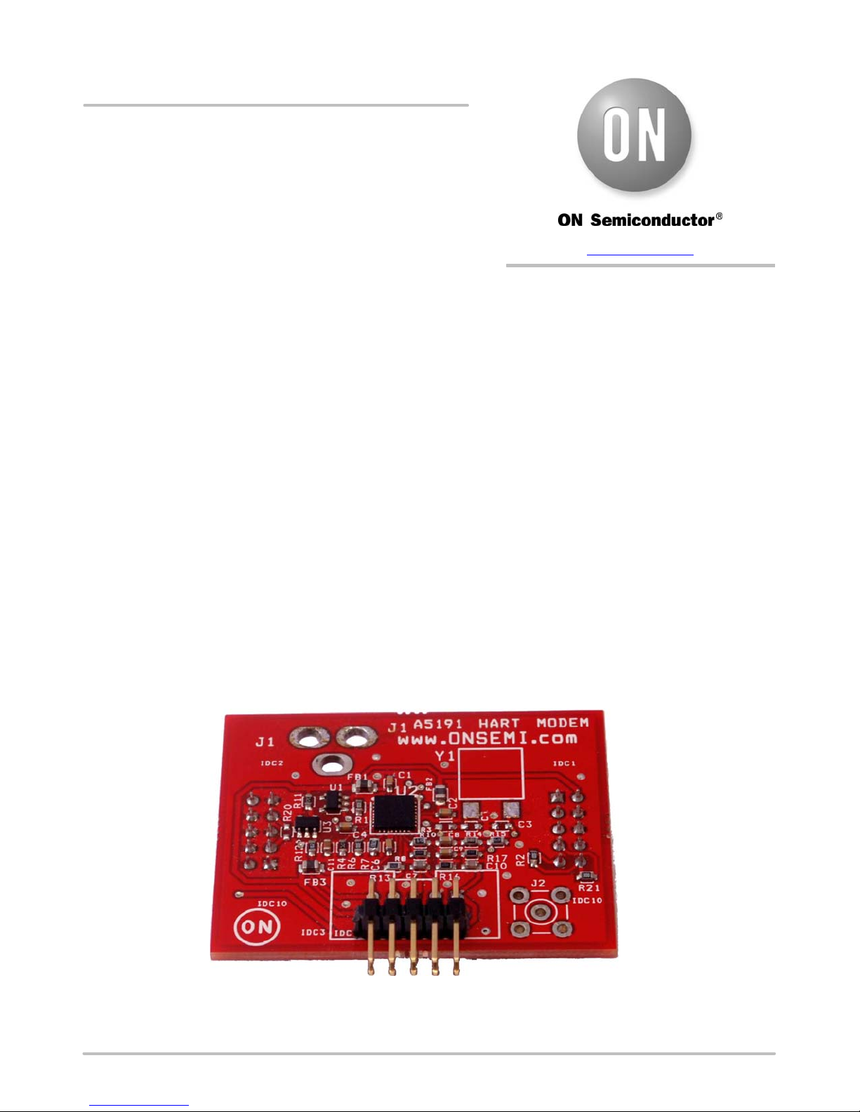
Figure 1. A5191HRTNGEVB Evaluation Board
1 Publication Order Number:
EVBUM2130/D
Page 2

A5191HRTNGEVB
ELECTRICAL CHARACTERISTICS
Table 1. ELECTRICAL CHARACTERISTICS OF THE A5191HRTNGEVB BOARD
Symbol Parameter / Condition
V
DD
CURRENT CONSUMPTION
I
DD
I
DD
I
DD
I
DD
TRANSMITTED FREQUENCY
f
M
f
S
LEVELS
V
TxA
V
CD
REFERENCE VOLTAGES
V
AREF
V
CDREF
Supply voltage 2.78 3 6.00 V
VDD = 2.78V, idle 417
VDD = 3.00 V, idle 420
VDD = 6.00V, idle 780
External clock, VDD = 3.00 V, idle 350
Mark “1” 1197 Hz
Space “0” 2194 Hz
Amplitude Transmit Output 500 mV
Carrier Detect Level 110 mV
AREF 1.212 V
CDREF 1.128 V
Min Typ Max
Value
Unit
mA
mA
mA
mA
pp
pp
A5191HRT DESCRIPTION
The A5191HRT modem is a single−chip CMOS modem
for use in HART field instruments and masters. It includes
on−chip oscillator and a modulator and demodulator module
communicating with a UART without internal buffer. The
A5191HRT requires some external filter components and a
460.8 kHz clock source. This clock source can either be the
interface oscillator by using a crystal or ceramic resonator,
When the device is transmitting data, the receive module
is shut down and vice versa to conserve power. With simple
power−saving maneuvers, the IC can be made to operate
with a current consumption of as little as 250 mA. For more
information related to this subject see the application note
AND9030 “A5191HRT Design for Low−Power
Environments”.
or an external clock signal.
TEST AND MEASUREMENT TOOLS
Listed below are the tools used to acquire the values presented in this Evaluation Board User’s Manual.
• Oscilloscope Tektronix DPO4034 350 MHz
• Signal Generator Agilent 33120A
• Network Analyzer AP Instruments 300
www.onsemi.com
2
Page 3

Schematic Diagram
A5191HRTNGEVB
A5191HRTNGEVB DESCRIPTION
Figure 2. Schematic of A5191HRTNEVB
www.onsemi.com
3
Page 4

A5191HRTNGEVB
BOM List
Table 2. A5191HRTNEVB BILL OF MATERIALS
Quantity Reference Value; Size Manufacturer & Comments
4 C1, C2, C4, C6 100 nF, 0603
3 C3, C5, C7 220 pF, 0603
2 C8, C9 1 nF, 0603
2 C10, C11 470 pF, 0603
3 FB1, FB2, FB3 600Z, 0805
3 IDC1, IDC2, IDC3 0.1” header, 10 pin
1 J1 Barrel connector Not populated
1 J2 SMB connector Not populated
4 R1, R2, R6, R21 200k, 0603
1 R3 0R, 0603
2 R4, R11 14k7, 0603
2 R7, R14 499k, 0603
3 R8, R16, R17 215k, 0603
1 R12 1k, 0603
1 R10 422k, 0603
1 R13 3M, 0603
1 R15 787k, 0603
1 R18 24k, 0603
1 R20 DNP, 0603 Not populated
1 U1 CAT808NTDI−27GT3 ON Semiconductor
1 U2 A5191HRT ON Semiconductor
1 U3 TLV431ASNT1G ON Semiconductor
1 Y1 460.8 kHz ECS Crystal ZTBF−460.8−E
General Overview
The A5191HRTNGEVB evaluation board demonstrates
the external components required for the operation of the IC.
We will cover the different sections below as well as possible
Figure 3. Board Drawing With Indication of Different Sections
alternatives. A drawing of the board where the different
sections are indicated is shown below.
www.onsemi.com
4
Page 5

Power Supply and References
Power Supply
A5191HRTNGEVB
Figure 4. Supply Voltage and Power on Reset
The A5191HRTNGEVB is designed for a nominal
voltage of 3 V. However, A5191HRT can be operated up to
6 V. For optimal functioning of the board, the values of
several resistors should be changed for operation at voltages
Current consumption of the module is very limited,
making it ideal to be battery or loop−powered.
Measurements of the power consumption of the module are
listed in Table 3.
higher than 3 V. See the sections on reference voltages and
bias for more information on this.
Table 3. MODULE CURRENT CONSUMPTION
Symbol Condition Current Consumption
I
DD
I
DD
I
DD
I
DD
I
DD
I
DD
I
DD
I
DD
The module will use less power when clock signal is
applied externally, as this allows the modem to shut down
the oscillator circuit. As is to be expected, a higher supply
voltage increases current consumption.
It is advised to use a voltage supervisor such as CAT808
to prevent the modem to begin operation when the supply
voltage is not yet reliable. This will guarantee correct
VDD = 2.78 V, Transmit
VDD = 2.78 V, Receive
VDD = 3 V, Transmit
VDD = 3 V, Receive
VDD = 6 V, Transmit
VDD = 6 V, Receive
VDD = 3 V, Transmit, Ext. Osc.
VDD = 3 V, Receive, Ext. Osc.
428 mA
417 mA
443 mA
419 mA
837 mA
781 mA
362 mA
350 mA
The voltage supervisor will keep the RESETB pin low
until its threshold value is reached (2.7 V on the
A5191HRTNGEVB). This ensures that some time has
passed after the supply voltage reaches the turn−on voltage
level of 2.5 V.
The RESETB and VDD pin signals during startup are
shown in Figure 5. The measured start−up delay is 2.6 ms.
operation of the digital circuitry.
www.onsemi.com
5
Page 6

A5191HRTNGEVB
Figure 5. Power and RESETB Waveform During Startup, Showing 2.63 ms Startup Delay
C1, C2 and C6 are 100 nF ceramic decoupling capacitors
located directly adjacent to each power pin. For analog
power pins, an additional large−value ceramic capacitor
may be needed in addition to the 100 nF decoupling
capacitor when the application is intended for high−noise
environments.
For loop powered devices, additional decoupling with a
large value capacitor is advised to prevent digital noise from
being transmitted on the current loop.
The ferrite beads FB1, FB2 and FB3 in series with power
supply lines help to reduce EMI.
Reference voltages and comparator bias
A5191HRT needs an external analog reference voltage
for the receiver or demodulator (RX) comparator and carrier
detect (CD).
The AREF reference voltage sets the trip point of the
demodulation operational amplifier of the 5191HRT. The
AREF reference voltage is also used in setting the DC
operating point of the received signal after it has passed
through the band−pass receive filter. The ideal value for the
AREF reference voltage depends on the voltage supply, and
is chosen roughly half−way the operating range of the
operational amplifiers. This ensures the range of the
operational amplifier is maximized. For operation at 3 V, a
1.24 V reference voltage is recommended. For operation at
5 V, a 2.5 V reference voltage is recommended.
For A5191HRTNGEVB, the TLV431 shunt regulator is
used with an internal reference of 1.24 V. This reference is
compared against the output voltage, and the shunt transistor
base is adjusted until it sinks enough current to drop the
output to 1.24 V.
A simple low pass filter formed by R12 and C11 is added
to increase reference stability. A slight voltage drop is
observed over this filter caused by loading of the reference
voltage. However, the voltage drop
and the influence on the
operation of the IC is minimal. Measurements show a
voltage drop of 22 mV over R12, indicating a current of 22
mA. Of this current ca. 5 mA is consumed by the CDREF
resistor division. The rest (ca. 17 mA) is used internally by
the IC through the AREF pin. Current consumption through
the CDREF pin is negligible.
The CDREF reference voltage sets the threshold for the
carrier detect comparator. As the received signal is biased at
AREF, the difference between CDREF and AREF will
determine the minimum amplitude needed for the carrier
detect comparator to flip. A (AREF−CDREF) of 80 mV
corresponds to signal of approximately 100 mV
peak−to−peak at the input of the receive filter. The CDREF
reference voltage on the A5191HRTNGEVB is generated
by a resistor division of the AREF reference. This will create
an extra load on the low pass filter of AREF. However, the
drop on the resistor of the low pass can be considered
negligible.
An external resistor is required to set the bias current. The
voltage over the bias resistor is regulated to AREF, so that
the resistor determines a bias current. This bias current
www.onsemi.com
6
Page 7

A5191HRTNGEVB
controls the operating parameters of the internal operational
amplifiers and comparators and should be set to
approximately 2.5 mA. A bias resistor of 499 kW is used on
the A5191HRTNGEVB. For low cost solutions, a 470 kW is
acceptable with minimal effect on operation.
Figure 6. Reference Voltages Schematic
Clock Generation
A5191HRT is operated on a 460.8 kHz clock signal. The
A5191HRTNGEVB has two options for providing this
clock signal. The first method is by using a ceramic
resonator or a crystal, for example ECS Crystal
ZTBF−460.8−E ceramic resonator, loaded with two 220 pF
capacitors.
Alternatively, a clock signal can be provided externally
when R3 is removed and C3 is replaced by a resistor o f 0 W.
This signal can be provided by a microcontroller or any other
external oscillator circuit. The module uses less power when
clock signal is applied externally, as this allows the modem
Table 4. REFERENCE VOLTAGES
Description Value
AREF reference voltage 1.212 V
CDREF reference voltage 1.128 V
Current through R
12
22 mA
to shut down the oscillator circuit. A typical current
consumption witnessed by utilizing an external oscillator is
70 − 100 mA less. However, care must be taken that this
external signal has the required accuracy (1%).
Duty cycle of the clock signal is specified between 40%
and 60%. No errors were observed during testing in
operation between 20% and 80% duty cycle. However,
operation on such very small or very large duty cycle is not
recommended, due to the possibility of timing errors that
may occur under specific circumstances (including, but not
limited to, temperature variations).
a.) Resonator Option b.) External Clock Option
Figure 7. Clock Generation Circuit
www.onsemi.com
7
Page 8

Microcontroller Interface IDC1
A5191HRTNGEVB
V
CC
R
2
V
CC
IDC
1
9
7
5
3
2
1
RESET
R
23
RTS
22
TxD
23
RxD
25
CD
26
PC20110513.4
Figure 8. Microcontroller Interface
Table 5. MICROCONTROLLER INTERFACE
Pin Number Signal Type Description
1 RST Open drain Reset signal from the voltage supervisor, open drain with pull−up
3 CD Output Carrier Detect
5 RxD Input Receive from microcontroller
7 TxD Output Transmit towards microcontroller
9 RTSB Input Request to send
2, 10 VDD Power 3 V nominal
4, 6, 8 GND Power
The interface towards a microcontroller is provided in
IDC1. This interface can also be used to supply power to the
module. The nominal supply voltage for the module is 3 V.
For more information see the section on power supply and
references.
The RESETB line to the modem is an open drain signal.
A pull−up resistor of 200 kW is provided on the board, and
should not be duplicated on the microcontroller side. The
reset signal is generated on the board, and could be used as
reset signal for other IC such as the microcontroller.
The CD signal rises when a HART signal of ca. 100 mV
pp
is detected on the current loop. See the section on reference
voltages for more information on these threshold level
settings. When no signal, or a signal of limited amplitude is
present, the CD line is pulled down to 0 V.
The RxD, TxD, and RTSB signals implement a standard
UART interface at 1200 baud with start bit 8 data bits, parity
bit and stop bit (1 1−bit frame). The RTSB signal disconnects
the transmitter circuit when pulled high, and should be held
low before any data is transmitted. Data frames are not
buffered by the modem. Instead, data is transmitted bit by
bit. Care should be taken to avoid clock skew in the receiving
UART. If the same time base is used for both the modem and
the UART, a 1% accurate time base may not be sufficient.
The problem is a combination of receive data jitter and clock
skew between transmitting and receiving HART devices. If
the transmit time base is at 99% of nominal and the receive
time base in another device is at 101% of nominal, the
receive data (at the receiving UART) will be skewed by
roughly 21% of one bit time at the end of each 11−bit byte.
This is shown in Figure 9. The skew time is measured from
the initial falling edge of the start bit to the center of the 11th
bit cell. This 21% skew by itself is a relatively good result.
However, there is another error source for bit boundary jitter.
The Phase Lock Loop demodulator in the A5191HRT
produces jitter in the receive data that can be as large as 12%
of a bit time. Therefore, a bit boundary can be shifted by as
much as 24% of a bit time relative to its ideal location based
on the start−bit transition. (The start−bit transition and a later
transition can be shifted in opposite directions for a total of
24%.)
The clock skew and jitter added together is 45%, which is
the amount that a bit boundary could be shifted from its
expected position. UARTs that sample at mid−bit will not be
affected. However, there are UARTs that take multiple
samples during each bit to try to improve on error
performance. These UARTs may not be satisfactory,
depending on how close the samples are to each other, and
how samples are interpreted. A UART that takes a majority
vote of three samples is acceptable.
www.onsemi.com
8
Page 9

A5191HRTNGEVB
Figure 9. Clock Skew
Even if your own time base is perfect, you still must plan
on a possible 35% shift in a bit boundary, since you don’t
have control over time bases in other HAR T devices.
Transmitter
The TxA modem pin is decoupled through a 100 nF
capacitor to pin 7 of IDC2. For certain applications, it might
be required to remove this capacitor and replace it by a 0 W
resistor. The output on this pin is a 500 mVpp signal
trapezoid waveform shown in Figures 10 and 11. This pin
can only drive impedances higher than 30 kW, and as a
consequence may need to be amplified to drive low
impedances. For a given implementation of a master or
slave, it may be required to remove C4 and replace it with a
0 W resistor to allow the decoupling to occur elsewhere in
the master implementation.
The nominal frequency of the output is 1196.9 Hz for
“mark” and 2194.3 Hz for “space”. These frequencies are
dependent on the accuracy of the A5191 clock.
Figure 10. Output Waveform (Mark)
www.onsemi.com
9
Page 10

A5191HRTNGEVB
Figure 11. Output Waveform (Space)
Receiver
The receive band pass filter is implemented on the
A5191HRTNGEVB. The values are listed in Table 6 and the
filter schematic is displayed in Figure 12. For cost purposes,
this filter can be implemented using E12 value resistors with
minimal changes to the filter characteristic. This
implementation will have a slightly reduced gain in the pass
band.
Figure 12. Receive Filter
www.onsemi.com
10
Page 11

A5191HRTNGEVB
Table 6. RECEIVE FILTER COMPONENT VALUES
Reference Value E96
R
16
R
17
R
14
R
15
R
10
R
8
R
13
C
10
C
8
C
9
C
7
215 kW 1% 220 kW 1%
215 kW 1% 220 kW 1%
499 kW 1% 470 kW 1%
787 kW 1% 680 kW 1%
422 kW 1% 470 kW 1%
215 kW 1% 220 kW 1%
3 MW 1% 3.3 MW 1%
470 pF 5% 470 pF 5%
1 nF 5% 1 nF 5%
1 nF 5% 1 nF 5%
220 pF 5% 220 pF 5%
Value E12
(Low−cost)
Figure 13. Filter Characteristic (First Stage = black, Total = Blue)
In Figure 13 the simulated characteristic of the entire filter
is shown, in both variations, for the first stage (black) and
total filter (blue). The normal and low−cost variations are
superimposed, showing that the variations are minimal.
However, when the tolerance on the values is also loosened,
a bigger variation in the characteristic is observed.
Figures 14a and 14b show a monte carlo analysis for
resistors of 1% and 10%. It is advised to use resistors of at
least 1% accuracy.
www.onsemi.com
11
Page 12

A5191HRTNGEVB
Figure 14. Monte Carlo Analysis of the First Filter Stage for 10% (above) and 1% (below) Accuracy
In Figure 15 the measured filter characteristic of both
variations are shown next to a simulated result. These
characteristics are only of the first stage of the filter as the
output of the second stage is not accessible. We notice an
additional pole showing up at high frequencies. This only
improves the filter by rejecting high frequency noise, and is
Figure 15. Measured and Simulated Filter Characteristic of the First Filter Stage
too high in frequency to have an influence on the phase of
HART signals. Figure 16 shows the group delay of the total
filter. It is important that the difference in group delay
between the mark and space is minimal, so that the output of
the filter still has coherence between both signals. The plot
of Figure 16 shows that the difference is indeed minimal.
www.onsemi.com
12
Page 13

A5191HRTNGEVB
Figure 16. Group Delay of the Total Filter
First Stage
The first stage of the filter is implemented as a modified
third−order high pass active filter.
Consider the circuit shown in Figure 17. This resembles
the implemented filter except for the coupling capacitor on
Figure 17. Simplified First Filter Stage Schematic
the operational amplifier, and the removal of R14. The filter
is a variation on the Sallen−Key topology with three poles.
The AREF voltage serves here as a biasing voltage, but can
for ac frequencies be regarded as ground. For a complete
analysis of this filter type, see the Appendix on Page 17.
www.onsemi.com
13
Page 14

A5191HRTNGEVB
The transfer function of this type of filter is:
Taking into account the compensation capacitance
present on the operational amplifier between input and
output introduces another high frequency pole and zero pair .
The zero of which can easily be determined to be:
Determining the exact location of the extra pole requires
extra calculation. Indeed, the location of the other poles will
also be shifted by this extra circuit element.
Introducing R
does not introduce another pole or zero
14
but changes the denominator of the transfer function, and
thus the location of the poles.
The final transfer function of the first filter stage is thus a
fourth order filter of the form:
The poles of this transfer function are located at:
, p2 = 195 Hz
p
1
p
= 1.220 kHz
3
p
= 22 kHz
4
The input impedance of this filter stage is higher than
89 kW at frequencies below 50 kHz.
Figure 18. Input Impedance of the First Filter Stage
Second Stage
The second stage of the receive filter is a simple band pass
filter consisting of cascaded passive low− and high−pass
filter.
AREF
R
2
R
1
Stage1 V
C
1
KVDE20110406.4
Figure 19. Second Filter Stage Schematic
C
2
out
www.onsemi.com
Again the AREF voltage can be considered ground for AC
frequencies, and serves only to bias the output of the filter
around AREF. It can be shown that this stage has the
following transfer function:
This stage has two poles that can easily be calculated:
p
= 36 Hz
1
p
= 3316 Hz
2
14
Page 15

A5191HRTNGEVB
Figure 20. Characteristic of the Second Stage of the Filter
APPLICATION IDEAS
The A5191HRT takes care of the HART modulation. This
HART signal must then be superimposed on a 4−20mA
current loop. Below are some possible implementations of
both a master and slave transmitter.
Slave implementation
A simple slave implementation is shown in Figure 21. The
analog loop current is set by a DAC from the
microcontroller, while HART signals are added in from the
A5191HRT. The DAC can be PWM or sigma−delta
topology . To explain the operation of this circuit, let us first
look at an example where the DAC is not of a switching
topology . I n this case, R
C
can be left out. As one end of R6 is tied to local ground,
5
and R3 can be 0 W, and C2, C3 and
2
it can easily be seen that the voltage at the negative loop
terminal is negative with respect to the local ground.
Resistors R
and R5 are then chosen so that in steady state
4
their common terminal is a virtual ground point in the
absence of HA RT signals, since the negative terminal of the
amplifier is also connected to ground. A similar principle
applies when HART signals are applied. So both amplifier
inputs are regulated to ground. A compensation capacitor C
may be required depending on the operational amplifier
used. To avoid offset generated by bias current in the
operational amp, R
should be dimensioned to approach the
3
impedance seen by the positive terminal.
The amplifier will then determine the current flowing
through the loop by changing the base of a transistor in
emitter feedback configuration. The value for R
determined by the output range V
of the amplifier used:
o,max
7
is
It is often recommended to take a value as large as
possible, so that noise effects are minimal.
Typically the value of R
voltage over R
and R7 combined should however be less
6
is chosen equal to R7. The
6
than 12 V when the current setting is 20 mA.
Next, the values of R
and R5 are chosen depending on the
4
most significant bit of the DAC.
When the DAC is not a switching topology, we can now
choose R
and C1. We have:
1
Where:
In practice, C1 is chosen sufficiently small so that Z [ R1.
For a PWM or sigma−delta output DAC, the circuit gets
a bit more complicated, as we need to filter away high
frequency DAC c o m ponents, but leave HART signals intact.
If the bandwidth of the DAC is larger than 2.2 kHz, adding
C
introduces a low−pass filter to the loop that will remove
3
most of the switching noise.
4
Where Rp is the parallel circuit of R4, R5 and R1.
If the bandwidth of the DAC is close to the HART
frequencies, an alternate high−frequency feedback path
must be introduced so that HART signals are not removed
by the low pass filter of the DAC. The exact calculation of
component values in this case is more complicated.
However, it i s based on a similar principle, but now with two
summing junctions, for low−frequency and high−frequency
signals separated.
Resistor R
may be needed to compensate for amplifier
3
bias current. It is chosen so that its resistance is similar to
resistance seen on the positive terminal. Depending on the
amplifier used, it may also be required to provide a
compensation capacitance C
.
4
www.onsemi.com
15
Page 16

A5191HRTNGEVB
Figure 21. Sample Slave Implementation
Master Implementation
An example of a possible master implementation is shown
in Figure 22. To use this schematic, the coupling capacitor
C4 on the A5191HRTNGEVB will need to be replaced by
a 0 W resistor, or new biasing must be provided.
The current loop master has a sense resistor over which the
current flowing through the loop can be measured. The value
of this resistor varies depending on the sensitivity required
and range of the ADC. A HART Master can have a sense
resistor ranging from 230 W
resistor will result in higher amplitude HART signal
received, but will also reduce the voltage available on the
slave side. Furthermore, if you wish to sense the analog
transmitted signal, the MSB of your DAC may limit the
resistor size. If this limitation is too stringent, the sense
resistor can be split in two resistors, as shown in the figure,
effectively creating a resistor divider.
To transmit a HART signal, the TxA signal will need to be
amplified, as the A5191HRT transmit circuit can only drive
high impedance circuits (>30 kW). An additional
to 600 W. Increasing the sense
operational amplifier is required. Depending on the sense
resistor used, some gain or attenuation may be required to
get a 1 mA peak−to−peak HART output signal. This can be
accomplished by the resistors R
and R4. For a typical sense
3
resistor of 500 W, a unity gain suffices and a unity gain
operational amplifier configuration can be used instead.
The amplifier however has a low impedance output,
which cannot be paralleled with the sense resistor, as this
would cause problems when the slave is transmitting. This
problem is solved by adding a series switch (such as
MC74VHC1G66DTT1G), controlled by the RTS signal.
For a normally open switch, the nR TS signal as applied to the
A5191 must be inverted first. To reduce power usage, the
operational amplifier can be disabled when the transmitter
is turned off. This is both done by inserting PNP transistor
Q
on the VDD connection of the amplifier.
1
To couple the signal into the current loop, a single
capacitor was used. For other coupling techniques see
application note AND8346/D.
www.onsemi.com
16
Page 17

nRTS
A5191HRTNGEVB
3V
R
1
Q
1
R
7
AREF
TxA
ADC
2
R
3
OPA
U
1
U
C
1
R
4
R
Figure 22. Sample Master Implementation
APPENDIX
Calculation of a three Pole Sallen−Key High Pass Filter
The first stage of the receive filter uses a three pole active
high pass filter with a topology similar to the one shown in
Figure 17. We will derive the transfer function of this filter
below. We will denote the gain configured with R
and R
A
input in DC, and can for the rest of the calculations be
considered parallel and replaced by one resistor:
B
as K.
Using Kirkhof’s current law, we get in the three nodes of the filter:
Loop +
C
2
2
R
5
R
6
Loop −
Resistors R3A and R3B serve only to bias the amplifier
Solving Equations 1 and 3 for V1 resp. V2 we find:
For Equation 2 we find:
Or, with the substitution:
(eq. 1)
(eq. 2)
(eq. 3)
(eq. 4)
(eq. 5)
(eq. 6)
www.onsemi.com
17
Page 18

A5191HRTNGEVB
Equation 6 simplifies to:
(eq. 7)
Substituting V1 and V2 in Equation 7 using Equations 4 and 5, and simplifying we find the transfer function:
Where:
Adding the compensation capacitor on the operational amplifier results in the following transformation on the transfer
function:
Where:
Since K is present in the numerator of the transfer
function, the zero of this factor will be present in the
transformed transfer function. The denominator of the
Where:
transformed transfer function is a forth order function with
the following coefficients.
The transfer function now has the following form:
www.onsemi.com
18
Page 19

A5191HRTNGEVB
Adding a series resistor to the capacitor results in the following transformation:
Since C3 is not present in the numerator or in the highest−order coefficient, no extra poles or zeros will be introduced by
this transformation. The form of the transfer function hence remains the same.
The transformed coefficients are:
www.onsemi.com
19
Page 20

A5191HRTNGEVB
P
al
EVALUATION BOARD LAYOUT
Figure 23. Top Layer Layout
HART is a registered trademark of the HART Communication Foundation of Austin, Texas, USA. Any time that the term ‘HART’ is used in
this document or in any document referenced by this document, that term implies the registered trademark.
ON Semiconductor and are trademarks of Semiconductor Components Industries, LLC dba ON Semiconductor or its subsidiaries in the United States and/or other countries.
ON Semiconductor owns the rights to a number of patents, trademarks, copyrights, trade secrets, and other intellectual property. A listing of ON Semiconductor ’s product/patent
coverage may be accessed at www.onsemi.com/site/pdf/Patent−Marking.pdf
ON Semiconductor makes no warranty, representation or guarantee regarding the suitability of its products for any particular purpose, nor does ON Semiconductor assume any liability
arising out of the application or use of any product or circuit, and specifically disclaims any and all liability, including without limitation special, consequential or incidental damages.
Buyer is responsible for its products and applications using ON Semiconductor products, including compliance with all laws, regulations and safety requirements or standards,
regardless of any support or applications information provided by ON Semiconductor. “Typical” parameters which may be provided in ON Semiconductor data sheets and/or
specifications can and do vary in different applications and actual performance may vary over time. All operating parameters, including “Typicals” must be validated for each customer
application by customer’s technical experts. ON Semiconductor does not convey any license under its patent rights nor the rights of others. ON Semiconductor products are not
designed, intended, or authorized for use as a critical component in life support systems or any FDA Class 3 medical devices or medical devices with a same or similar classification
in a foreign jurisdiction or any devices intended for implantation in the human body. Should Buyer purchase or use ON Semiconductor products for any such unintended or unauthorized
application, Buyer shall indemnify and hold ON Semiconductor and its officers, employees, subsidiaries, affiliates, and distributors harmless against all claims, costs, damages, and
expenses, and reasonable attorney fees arising out of, directly or indirectly, any claim of personal injury or death associated with such unintended or unauthorized use, even if such
claim alleges that ON Semiconductor was negligent regarding the design or manufacture of the part. ON Semiconductor is an Equal Opportunity/Affirmative Action Employer. This
literature is subject to all applicable copyright laws and is not for resale in any manner.
UBLICATION ORDERING INFORMATION
LITERATURE FULFILLMENT:
Literature Distribution Center for ON Semiconductor
P.O. Box 5163, Denver, Colorado 80217 USA
Phone: 303−675−2175 or 800−344−3860 Toll Free USA/Canada
Fax: 303−675−2176 or 800−344−3867 Toll Free USA/Canada
Email: orderlit@onsemi.com
Figure 24. Bottom Layer Layout
. ON Semiconductor reserves the right to make changes without further notice to any products herein.
N. American Technical Support: 800−282−9855 Toll Free
USA/Canada
Europe, Middle East and Africa Technical Support:
Phone: 421 33 790 2910
Japan Customer Focus Center
Phone: 81−3−5817−1050
www.onsemi.com
20
ON Semiconductor Website: www.onsemi.com
Order Literature: http://www.onsemi.com/orderlit
For additional information, please contact your loc
Sales Representative
EVBUM2130/D
 Loading...