

Page 1
74FST3257
Quad 2:1 Multiplexer/
Demultiplexer Bus Switch
The ON Semiconductor 74FST3257 is a quad 2:1, high performance
multiplexer/demultiplexer bus switch. The device is CMOS TTL
compatible when operating between 4 and 5.5 Volts. The device
exhibits extremely low R
The device adds no noise or ground bounce to the system.
Features
• R
t 4 W Typical
ON
• Less Than 0.25 ns−Max Delay Through Switch
• Nearly Zero Standby Current
• No Circuit Bounce
• Control Inputs are TTL/CMOS Compatible
• Pin−For−Pin Compatible With QS3257, FST3257, CBT3257
• All Popular Packages: SOIC−16, TSSOP−16, QFN16
• NLV Prefix for Automotive and Other Applications Requiring
Unique Site and Control Change Requirements; AEC−Q100
Qualified and PPAP Capable
• These Devices are Pb−Free, Halogen Free/BFR Free and are RoHS
Compliant
and adds nearly zero propagation delay.
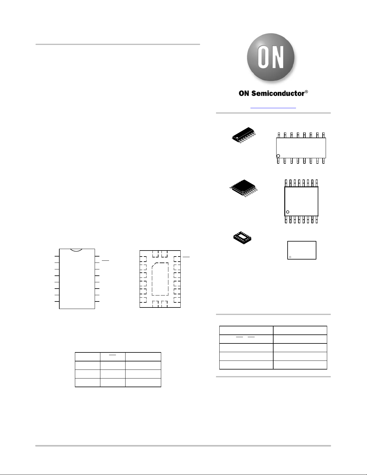
ON
16
SOIC−16
D SUFFIX
CASE 751B
16
TSSOP−16
DT SUFFIX
CASE 948F
www.onsemi.com
16
1
1
MARKING
DIAGRAMS
FST3257G
AWLYWW
1
16
FST
3257
ALYW G
G
1
SV
1
1B
2
1
1B
3
2
1A
4
2B
5
1
2B
6
2
2A
7
GND 3A
89
16
15
14
13
12
11
10
OE
4B
4B
4A
3B
3B
CC
1B
1
2
1
2
1B
1A
2B
2B
2A
Figure 1. 16−Lead Pinout Diagrams
S
X
L
H
OE
H
L
L
Function
Disconnect
Figure 2. Truth Table
2
1
3
2
4
5
1
6
2
7
A = B
A = B
V
S
CC
1
16
GND
89
GND 3A
1
2
15
14
13
12
11
10
OE
4B
4B
4A
3B
3B
1
QFN16
MN SUFFIX
1
2
1
2
CASE 485AW
A = Assembly Location
WL, L = Wafer Lot
Y = Year
WW, W = Work Week
G or G = Pb−Free Package
(Note: Microdot may be in either location)
3257
ALYWG
G
PIN NAMES
Pin
OE1, OE
B1, B2, B3, B
2
S0, S
1
A Bus A
4
Description
Bus Switch Enables
Select Inputs
Bus B
ORDERING INFORMATION
See detailed ordering and shipping information in the package
dimensions section on page 2 of this data sheet.
© Semiconductor Components Industries, LLC, 2011
May, 2018 − Rev. 8
1 Publication Order Number:
74FST3257/D
Page 2
74FST3257
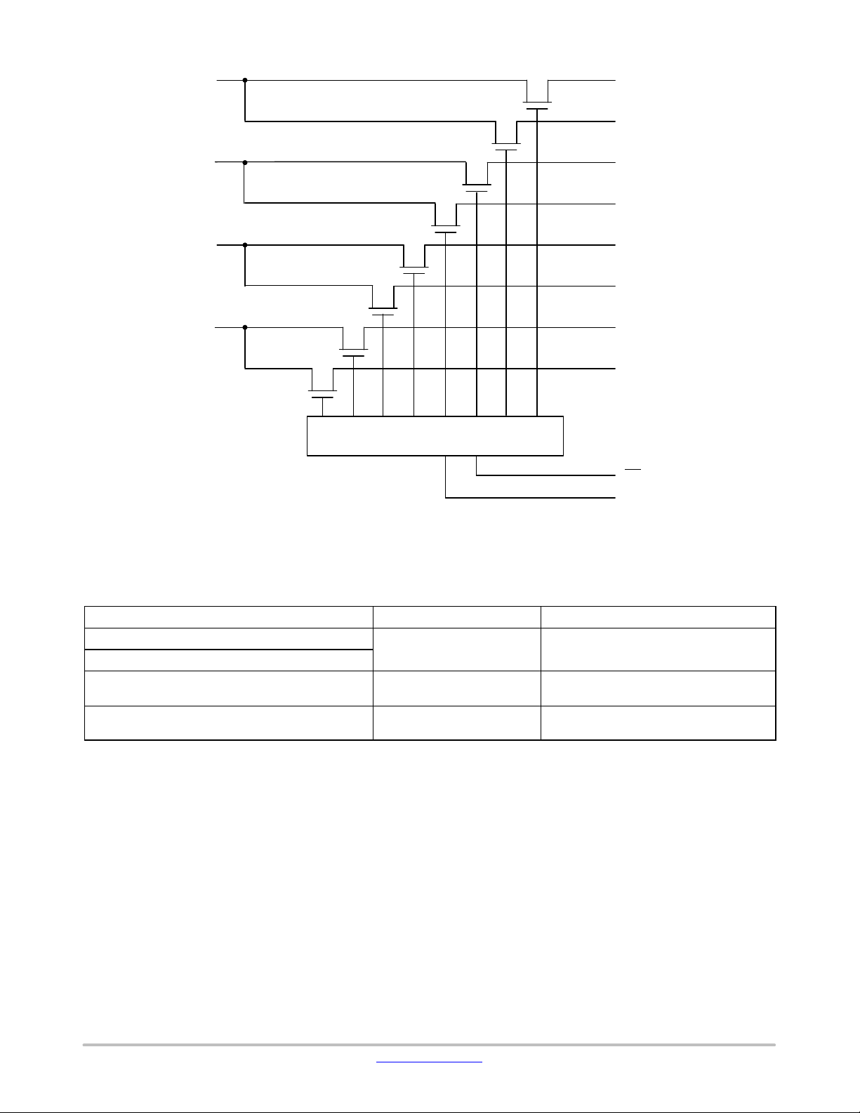
1A
2A
3A
4A
FLOW CONTROL
1B
1B
2B
2B
3B
3B
4B
4B
OE
S
2
1
2
1
2
1
2
Figure 3. Logic Diagram
ORDERING INFORMATION
Device Order Number Package Shipping
74FST3257DR2G
NLV74FST3257DR2G*
74FST3257DTR2G TSSOP−16
SOIC−16
(Pb−Free)
2500 Units / Tape & Reel
2500 Units / Tape & Reel
(Pb−Free)
74FST3257MNTWG QFN16
3000 Units / Tape & Reel
(Pb−Free)
†For information on tape and reel specifications, including part orientation and tape sizes, please refer to our Tape and Reel Packaging
Specifications Brochure, BRD8011/D.
*NLV Prefix for Automotive and Other Applications Requiring Unique Site and Control Change Requirements; AEC−Q100 Qualified and PPAP
Capable.
†
www.onsemi.com
2
Page 3
74FST3257
MAXIMUM RATINGS
Symbol Parameter Value Units
V
CC
V
V
I
IK
I
OK
I
O
I
CC
I
GND
T
STG
T
T
q
JA
MSL Moisture Sensitivity Level 1
F
V
ESD
I
Latchup
Stresses exceeding those listed in the Maximum Ratings table may damage the device. If any of these limits are exceeded, device functionality
should not be assumed, damage may occur and reliability may be affected.
1. Tested to EIA/JESD22−A114−A.
2. Tested to EIA/JESD22−A115−A.
3. Tested to JESD22−C101−A.
4. Tested to EIA/JESD78.
DC Supply Voltage −0.5 to +7.0 V
DC Input Voltage −0.5 to +7.0 V
I
DC Output Voltage −0.5 to +7.0 V
O
DC Input Diode Current
V
t GND −50
I
DC Output Diode Current
V
t GND −50
O
DC Output Sink Current 128 mA
DC Supply Current per Supply Pin ±100 mA
DC Ground Current per Ground Pin ±100 mA
Storage Temperature Range −65 to +150
Lead Temperature, 1 mm from Case for 10 Seconds 260
L
Junction Temperature Under Bias +150
J
Thermal Resistance
Flammability Rating
R
SOIC
TSSOP
QFN
Oxygen Index: 28 to 34
UL 94 V−0 @ 0.125 in
125
170
N/A
ESD Withstand Voltage
Human Body Model (Note 1)
Machine Model (Note 2)
Charged Device Model (Note 3)
u2000
u200
N/A
Latchup Performance
Above V
and Below GND at 85_C (Note 4)
CC
±500
mA
mA
_C
_C
_C
_C/W
V
mA
RECOMMENDED OPERATING CONDITIONS
Symbol Parameter Min Max Units
V
CC
V
V
T
Dt/DV
Supply Voltage
Operating, Data Retention Only
Input Voltage (Note 5) 0 5.5 V
I
Output Voltage (HIGH or LOW State) 0 5.5 V
O
Operating Free−Air Temperature −40 +85
A
4.0 5.5
Input Transition Rise or Fall Rate Switch Control Input
Switch I/O V
= 5.0 V ± 0.5 V
CC
0
DC
5
5. Unused control inputs may not be left open. All control inputs must be tied to a high or low logic input voltage level.
www.onsemi.com
3
V
_C
ns/V
Page 4

74FST3257
DC ELECTRICAL CHARACTERISTICS
V
CC
Symbol Parameter Conditions (V) Min Typ* Max Units
V
V
V
I
R
Clamp Diode Voltage IIN = −18 mA 4.5 −1.2 V
IK
High−Level Input Voltage 4.0 to 5.5 2.0 V
IH
Low−Level Input Voltage 4.0 to 5.5 0.8 V
IL
I
Input Leakage Current 0 ≤ VIN ≤ 5.5 V 5.5 ±1.0
I
Off−State Leakage Current 0 ≤ A, B ≤ V
OZ
Switch On Resistance (Note 6) VIN = 0 V, IIN = 64 mA 4.5 4 7
ON
CC
5.5 ±1.0
VIN = 0 V, IIN = 30 mA 4.5 4 7
VIN = 2.4 V, IIN = 15 mA 4.5 8 15
VIN = 2.4 V, IIN = 15 mA 4.0 11 20
I
DI
Quiescent Supply Current VIN = VCC or GND, I
CC
Increase In ICC per Input One input at 3.4 V,
CC
Other inputs at V
= 0 5.5 3
OUT
5.5 2.5 mA
or GND
CC
*Typical values are at VCC = 5.0 V and TA = 25_C.
6. Measured by the voltage drop between A and B pins at the indicated current through the switch. On resistance is determined by the lower
of the voltages on the two (A or B) pins.
TA = −40_C to +85_C
mA
mA
W
mA
AC ELECTRICAL CHARACTERISTICS
TA = −40_C to +85_C
C
= 50 pF, RU = RD = 500 W
L
VCC = 4.5−5.5 V VCC = 4.0 V
Symbol Parameter Conditions Min Max Min Max Units
t
PHL
t
t
PZH
t
t
PHZ
t
PLH
PZL
PLZ
,
Prop Delay Bus to Bus (Note 7)
Prop Delay, Select to Bus A 1.0 4.7 5.2
,
Output Enable Time, Select to Bus B VI = 7 V for t
Output Enable Time, IOE to Bus A, B VI = OPEN for t
,
Output Disable Time, Select to Bus B VI = 7 V for t
Output Disable Time, IOE to Bus A, B VI = OPEN for t
VI = OPEN
PZL
PLZ
PZH
PHZ
0.25 0.25
1.0 5.2 5.7
1.0 5.1 5.6
1.0 5.2 5.5
1.0 5.5 5.5
ns
ns
ns
7. This parameter is guaranteed by design but is not tested. The bus switch contributes no propagation delay other than the RC delay of the
typical On resistance of the switch and the 50 pF load capacitance, when driven by an ideal voltage source (zero output impedance).
CAPACITANCE (Note 8)
Symbol
C
C
C
Control Pin Input Capacitance VCC = 5.0 V 3 pF
IN
A Port Input/Output Capacitance VCC, OE = 5.0 V 7 pF
I/O
B Port Input/Output Capacitance VCC, OE = 5.0 V 5 pF
I/O
8. TA = )25_C, f = 1 MHz, Capacitance is characterized but not tested.
Parameter Conditions Typ Max Units
www.onsemi.com
4
Page 5
74FST3257
AC Loading and Waveforms
V
I
FROM
OUTPUT
UNDER
TEST
CL*
NOTES:
1. Input driven by 50 W source terminated in 50 W.
2. CL includes load and stray capacitance.
*C
= 50 pF
L
Figure 4. AC Test Circuit
t
= 2.5 nS
f
90 %
SWITCH
INPUT
OUTPUT
90 %
10 % 10 %
t
PLH
1.5 V 1.5 V
500 W
500 W
t
= 2.5 nS
f
3.0 V
1.5 V1.5 V
GND
t
PLH
V
OH
V
OL
ENABLE
INPUT
t
= 2.5 nS
f
OUTPUT
OUTPUT
Figure 5. Propagation Delays
90 %
t
PZL
t
PZH
1.5 V
10 %10 %
1.5 V
1.5 V
90 %
1.5 V
Figure 6. Enable/Disable Delays
t
= 2.5 nS
f
t
PLZ
t
PHZ
3.0 V
GND
V
OL
V
OL
V
OH
V
OH
+ 0.3 V
− 0.3 V
www.onsemi.com
5
Page 6

MECHANICAL CASE OUTLINE
PACKAGE DIMENSIONS
1
SCALE 2:1
16X
2X
2X
NOTE 4
PIN ONE
REFERENCE
C0.10
C0.08
L
16X
DETAIL A
C0.15
C0.15
TOP VIEW
DETAIL B
SIDE VIEW
2
1
e
e/2
BOTTOM VIEW
D
D2
8
0.15
10
15
A
B
E
A
(A3)
A1
C A B
K
0.15
E2
QFN16, 2.5x3.5, 0.5P
CASE 485AW−01
ISSUE O
L1
DETAIL A
ALTERNATE TERMINAL
CONSTRUCTIONS
DETAIL B
ALTERNATE
CONSTRUCTIONS
SEATING
C
PLANE
C A B
16X
b
0.10 C
A B
0.05
C
NOTE 3
DATE 11 DEC 2008
NOTES:
1. DIMENSIONING AND TOLERANCING PER
L
MOLD CMPDEXPOSED Cu
L
ASME Y14.5M, 1994.
2. CONTROLLING DIMENSION: MILLIMETERS.
3. DIMENSIONS b APPLIES TO PLATED
TERMINAL AND IS MEASURED BETWEEN
0.15 AND 0.30 MM FROM TERMINAL.
4. COPLANARITY APPLIES TO THE EXPOSED
PAD AS WELL AS THE TERMINALS.
MILLIMETERS
DIM MIN MAX
A
0.80 1.00
A1 0.00 0.05
A3
0.20 REF
b 0.20 0.30
D 2.50 BSC
D2 0.85 1.15
E 3.50 BSC
E2
1.85 2.15
e 0.50 BSC
K 0.20 ---
L 0.35 0.45
L1 --- 0.15
GENERIC MARKING
DIAGRAM*
XXXX
ALYWG
G
XXXX = Specific Device Code
A = Assembly Location
L = Wafer Lot
Y = Year
W = Work Week
G = Pb−Free Package
(Note: Microdot may be in either location)
*This information is generic. Please refer to
device data sheet for actual part marking.
Pb−Free indicator, “G” or microdot “ G”,
may or may not be present.
SOLDERING FOOTPRINT*
3.80
2.10
0.50
PITCH
2.80
1.10
1
PACKAGE
16X
0.60
16X
0.30
DIMENSIONS: MILLIMETERS
OUTLINE
*For additional information on our Pb−Free strategy and soldering
details, please download the ON Semiconductor Soldering and
Mounting Techniques Reference Manual, SOLDERRM/D.
DOCUMENT NUMBER:
DESCRIPTION:
ON Semiconductor and are trademarks of Semiconductor Components Industries, LLC dba ON Semiconductor or its subsidiaries in the United States and/or other countries.
ON Semiconductor reserves the right to make changes without further notice to any products herein. ON Semiconductor makes no warranty, representation or guarantee regarding
the suitability of its products for any particular purpose, nor does ON Semiconductor assume any liability arising out of the application or use of any product or circuit, and specifically
disclaims any and all liability, including without limitation special, consequential or incidental damages. ON Semiconductor does not convey any license under its patent rights nor the
rights of others.
© Semiconductor Components Industries, LLC, 2019
98AON36347E
QFN16, 2.5X3.5, 0.5P
Electronic versions are uncontrolled except when accessed directly from the Document Repository.
Printed versions are uncontrolled except when stamped “CONTROLLED COPY” in red.
PAGE 1 OF 1
www.onsemi.com
Page 7
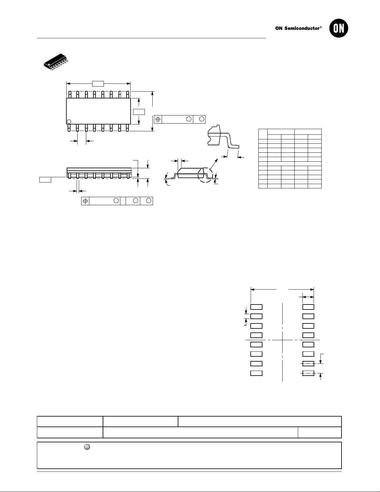
MECHANICAL CASE OUTLINE
PACKAGE DIMENSIONS
SCALE 1:1
−A−
16 9
−B−
18
G
K
C
−T−
SEATING
PLANE
D
16 PL
0.25 (0.010) A
M
S
B
T
S
CASE 751B−05
8 PLP
0.25 (0.010) B
M
SOIC−16
ISSUE K
M
R
X 45
DATE 29 DEC 2006
NOTES:
1. DIMENSIONING AND TOLERANCING PER ANSI
Y14.5M, 1982.
2. CONTROLLING DIMENSION: MILLIMETER.
3. DIMENSIONS A AND B DO NOT INCLUDE MOLD
PROTRUSION.
4. MAXIMUM MOLD PROTRUSION 0.15 (0.006) PER SIDE.
5. DIMENSION D DOES NOT INCLUDE DAMBAR
S
_
F
J
PROTRUSION. ALLOWABLE DAMBAR PROTRUSION
SHALL BE 0.127 (0.005) TOTAL IN EXCESS OF THE D
DIMENSION AT MAXIMUM MATERIAL CONDITION.
DIM MIN MAX MIN MAX
A 9.80 10.00 0.386 0.393
B 3.80 4.00 0.150 0.157
C 1.35 1.75 0.054 0.068
D 0.35 0.49 0.014 0.019
F 0.40 1.25 0.016 0.049
G 1.27 BSC 0.050 BSC
J 0.19 0.25 0.008 0.009
K 0.10 0.25 0.004 0.009
M 0 7 0 7
____
P 5.80 6.20 0.229 0.244
R 0.25 0.50 0.010 0.019
INCHESMILLIMETERS
STYLE 1:
PIN 1. COLLECTOR
2. BASE
3. EMITTER
4. NO CONNECTION
5. EMITTER
6. BASE
7. COLLECTOR
8. COLLECTOR
9. BASE
10. EMITTER
11. NO CONNECTION
12. EMITTER
13. BASE
14. COLLECTOR
15. EMITTER
16. COLLECTOR
STYLE 5:
PIN 1. DRAIN, DYE #1
2. DRAIN, #1
3. DRAIN, #2
4. DRAIN, #2
5. DRAIN, #3
6. DRAIN, #3
7. DRAIN, #4
8. DRAIN, #4
9. GATE, #4
10. SOURCE, #4
11. GATE, #3
12. SOURCE, #3
13. GATE, #2
14. SOURCE, #2
15. GATE, #1
16. SOURCE, #1
STYLE 2:
PIN 1. CATHODE
2. ANODE
3. NO CONNECTION
4. CATHODE
5. CATHODE
6. NO CONNECTION
7. ANODE
8. CATHODE
9. CATHODE
10. ANODE
11. NO CONNECTION
12. CATHODE
13. CATHODE
14. NO CONNECTION
15. ANODE
16. CATHODE
STYLE 6:
PIN 1. CATHODE
2. CATHODE
3. CATHODE
4. CATHODE
5. CATHODE
6. CATHODE
7. CATHODE
8. CATHODE
9. ANODE
10. ANODE
11. ANODE
12. ANODE
13. ANODE
14. ANODE
15. ANODE
16. ANODE
STYLE 3:
PIN 1. COLLECTOR, DYE #1
2. BASE, #1
3. EMITTER, #1
4. COLLECTOR, #1
5. COLLECTOR, #2
6. BASE, #2
7. EMITTER, #2
8. COLLECTOR, #2
9. COLLECTOR, #3
10. BASE, #3
11. EMITTER, #3
12. COLLECTOR, #3
13. COLLECTOR, #4
14. BASE, #4
15. EMITTER, #4
16. COLLECTOR, #4
STYLE 7:
PIN 1. SOURCE N‐CH
2. COMMON DRAIN (OUTPUT)
3. COMMON DRAIN (OUTPUT)
4. GATE P‐CH
5. COMMON DRAIN (OUTPUT)
6. COMMON DRAIN (OUTPUT)
7. COMMON DRAIN (OUTPUT)
8. SOURCE P‐CH
9. SOURCE P‐CH
10. COMMON DRAIN (OUTPUT)
11. COMMON DRAIN (OUTPUT)
12. COMMON DRAIN (OUTPUT)
13. GATE N‐CH
14. COMMON DRAIN (OUTPUT)
15. COMMON DRAIN (OUTPUT)
16. SOURCE N‐CH
STYLE 4:
PIN 1. COLLECTOR, DYE #1
2. COLLECTOR, #1
3. COLLECTOR, #2
4. COLLECTOR, #2
5. COLLECTOR, #3
6. COLLECTOR, #3
7. COLLECTOR, #4
8. COLLECTOR, #4
9. BASE, #4
10. EMITTER, #4
11. BASE, #3
12. EMITTER, #3
13. BASE, #2
14. EMITTER, #2
15. BASE, #1
16. EMITTER, #1
SOLDERING FOOTPRINT
1
16X
0.58
89
8X
6.40
16X
1.12
16
DIMENSIONS: MILLIMETERS
1.27
PITCH
DOCUMENT NUMBER:
DESCRIPTION:
ON Semiconductor and are trademarks of Semiconductor Components Industries, LLC dba ON Semiconductor or its subsidiaries in the United States and/or other countries.
ON Semiconductor reserves the right to make changes without further notice to any products herein. ON Semiconductor makes no warranty, representation or guarantee regarding
the suitability of its products for any particular purpose, nor does ON Semiconductor assume any liability arising out of the application or use of any product or circuit, and specifically
disclaims any and all liability, including without limitation special, consequential or incidental damages. ON Semiconductor does not convey any license under its patent rights nor the
rights of others.
© Semiconductor Components Industries, LLC, 2019
98ASB42566B
SOIC−16
Electronic versions are uncontrolled except when accessed directly from the Document Repository.
Printed versions are uncontrolled except when stamped “CONTROLLED COPY” in red.
PAGE 1 OF 1
www.onsemi.com
Page 8

MECHANICAL CASE OUTLINE
PACKAGE DIMENSIONS
16
1
SCALE 2:1
16X REFK
M
G
0.10 (0.004)
−T−
SEATING
PLANE
L
U0.15 (0.006) T
PIN 1
IDENT.
U0.15 (0.006) T
D
S
2X L/2
S
0.10 (0.004) V
16
1
A
−V−
C
CASE 948F−01
U
T
9
B
−U−
8
TSSOP−16
ISSUE B
S
S
J
N
N
DETAIL E
H
J1
F
DETAIL E
K
K1
SECTION N−N
0.25 (0.010)
M
DATE 19 OCT 2006
NOTES:
1. DIMENSIONING AND TOLERANCING PER
ANSI Y14.5M, 1982.
2. CONTROLLING DIMENSION: MILLIMETER.
3. DIMENSION A DOES NOT INCLUDE MOLD
FLASH. PROTRUSIONS OR GATE BURRS.
MOLD FLASH OR GATE BURRS SHALL NOT
EXCEED 0.15 (0.006) PER SIDE.
4. DIMENSION B DOES NOT INCLUDE
INTERLEAD FLASH OR PROTRUSION.
INTERLEAD FLASH OR PROTRUSION SHALL
NOT EXCEED 0.25 (0.010) PER SIDE.
5. DIMENSION K DOES NOT INCLUDE DAMBAR
PROTRUSION. ALLOWABLE DAMBAR
PROTRUSION SHALL BE 0.08 (0.003) TOTAL
IN EXCESS OF THE K DIMENSION AT
MAXIMUM MATERIAL CONDITION.
6. TERMINAL NUMBERS ARE SHOWN FOR
REFERENCE ONLY.
7. DIMENSION A AND B ARE TO BE
DETERMINED AT DATUM PLANE −W−.
DIM MIN MAX MIN MAX
A 4.90 5.10 0.193 0.200
B 4.30 4.50 0.169 0.177
C −−− 1.20 −−− 0.047
D 0.05 0.15 0.002 0.006
F 0.50 0.75 0.020 0.030
G 0.65 BSC 0.026 BSC
H 0.18 0.28 0.007 0.011
−W−
J 0.09 0.20 0.004 0.008
J1 0.09 0.16 0.004 0.006
K 0.19 0.30 0.007 0.012
K1 0.19 0.25 0.007 0.010
L 6.40 BSC 0.252 BSC
M 0 8 0 8
____
INCHESMILLIMETERS
SOLDERING FOOTPRINT
7.06
GENERIC
MARKING DIAGRAM*
16
XXXX
1
XXXX
ALYW
1
XXXX = Specific Device Code
A = Assembly Location
L = Wafer Lot
Y = Year
0.65
PITCH
W = Work Week
G or G = Pb−Free Package
*This information is generic. Please refer to
16X
0.36
DOCUMENT NUMBER:
DESCRIPTION:
ON Semiconductor and are trademarks of Semiconductor Components Industries, LLC dba ON Semiconductor or its subsidiaries in the United States and/or other countries.
ON Semiconductor reserves the right to make changes without further notice to any products herein. ON Semiconductor makes no warranty, representation or guarantee regarding
the suitability of its products for any particular purpose, nor does ON Semiconductor assume any liability arising out of the application or use of any product or circuit, and specifically
disclaims any and all liability, including without limitation special, consequential or incidental damages. ON Semiconductor does not convey any license under its patent rights nor the
rights of others.
16X
1.26
98ASH70247A
TSSOP−16
DIMENSIONS: MILLIMETERS
Electronic versions are uncontrolled except when accessed directly from the Document Repository.
Printed versions are uncontrolled except when stamped “CONTROLLED COPY” in red.
device data sheet for actual part marking.
Pb−Free indicator, “G” or microdot “ G”,
may or may not be present.
PAGE 1 OF 1
© Semiconductor Components Industries, LLC, 2019
www.onsemi.com
Page 9

ON Semiconductor and are trademarks of Semiconductor Components Industries, LLC dba ON Semiconductor or its subsidiaries in the United States and/or other countries.
ON Semiconductor owns the rights to a number of patents, trademarks, copyrights, trade secrets, and other intellectual property. A listing of ON Semiconductor’s product/patent
coverage may be accessed at www.onsemi.com/site/pdf/Patent−Marking.pdf
ON Semiconductor makes no warranty, representation or guarantee regarding the suitability of its products for any particular purpose, nor does ON Semiconductor assume any liability
arising out of the application or use of any product or circuit, and specifically disclaims any and all liability, including without limitation special, consequential or incidental damages.
Buyer is responsible for its products and applications using ON Semiconductor products, including compliance with all laws, regulations and safety requirements or standards,
regardless of any support or applications information provided by ON Semiconductor. “Typical” parameters which may be provided in ON Semiconductor data sheets and/or
specifications can and do vary in different applications and actual performance may vary over time. All operating parameters, including “Typicals” must be validated for each customer
application by customer’s technical experts. ON Semiconductor does not convey any license under its patent rights nor the rights of others. ON Semiconductor products are not
designed, intended, or authorized for use as a critical component in life support systems or any FDA Class 3 medical devices or medical devices with a same or similar classification
in a foreign jurisdiction or any devices intended for implantation in the human body. Should Buyer purchase or use ON Semiconductor products for any such unintended or unauthorized
application, Buyer shall indemnify and hold ON Semiconductor and its officers, employees, subsidiaries, affiliates, and distributors harmless against all claims, costs, damages, and
expenses, and reasonable attorney fees arising out of, directly or indirectly, any claim of personal injury or death associated with such unintended or unauthorized use, even if such
claim alleges that ON Semiconductor was negligent regarding the design or manufacture of the part. ON Semiconductor is an Equal Opportunity/Affirmative Action Employer. This
literature is subject to all applicable copyright laws and is not for resale in any manner.
. ON Semiconductor reserves the right to make changes without further notice to any products herein.
PUBLICATION ORDERING INFORMATION
LITERATURE FULFILLMENT:
Email Requests to: orderlit@onsemi.com
ON Semiconductor Website: www.onsemi.com
TECHNICAL SUPPORT
North American Technical Support:
Voice Mail: 1 800−282−9855 Toll Free USA/Canada
Phone: 011 421 33 790 2910
Europe, Middle East and Africa Technical Support:
Phone: 00421 33 790 2910
For additional information, please contact your local Sales Representative
◊
www.onsemi.com
1
 Loading...