

Page 1
2SA1774G, S2SA1774G
PNP Silicon General
Purpose Amplifier Transistor
This PNP transistor is designed for general purpose amplifier
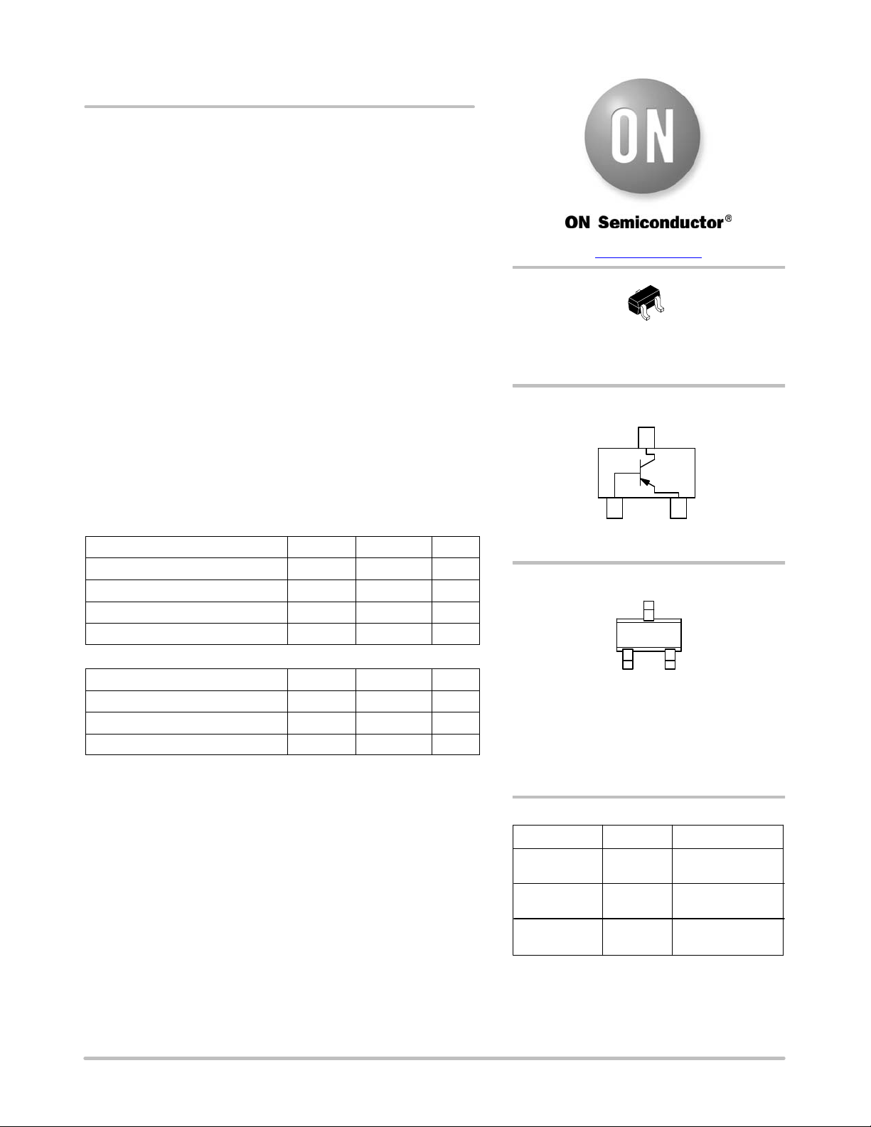
applications. This device is housed in the SC−75/SOT−416/SC−90
package which is designed for low power surface mount
applications, where board space is at a premium.
Features
• Reduces Board Space
• High h
• Low V
• Available in 8 mm, 7−inch/3000 Unit Tape and Reel
• S Prefix for Automotive and Other Applications Requiring Unique
Site and Control Change Requirements; AEC−Q101 Qualified and
PPAP Capable
• These Devices are Pb−Free, Halogen Free/BFR Free and are RoHS
Compliant*
, 210−460 (typical)
FE
, < 0.5 V
CE(sat)
www.
CASE 463
COLLECTOR
onsemi.com
SC−75
STYLE 1
3
MAXIMUM RATINGS (T
Rating Symbol Value Unit
Collector − Emitter Voltage V
Collector − Base Voltage V
Emitter − Base Voltage V
Collector Current − Continuous I
= 25°C)
A
(BR)CBO
(BR)CEO
(BR)EBO
C
−60 Vdc
−50 Vdc
−6.0 Vdc
−100 mAdc
THERMAL CHARACTERISTICS
Characteristic Symbol Max Unit
Power Dissipation (Note 1) P
Junction Temperature T
Storage Temperature Range T
Stresses exceeding those listed in the Maximum Ratings table may damage the
device. If any of these limits are exceeded, device functionality should not be
assumed, damage may occur and reliability may be affected.
1. Device mounted on a FR−4 glass epoxy printed circuit board using the
minimum recommended footprint.
*For additional information on our Pb−Free strategy and soldering details, please
download the ON Semiconductor Soldering and Mounting Techniques Reference
Manual, SOLDERRM/D.
D
J
stg
150 mW
150 °C
−55 ~ + 150 °C
1
BASE
2
EMITTER
MARKING DIAGRAM
F9 M G
G
1
F9 = Device Code
M = Date Code*
G = Pb−Free Package
(Note: Microdot may be in either location)
*Date Code orientation may vary depending
upon manufacturing location.
ORDERING INFORMATION
Device Package Shipping
2SA1774G SC−75
(Pb−Free)
S2SA1774G SC−75
(Pb−Free)
2SA1774T1G SC−75
(Pb−Free)
†For information on tape and reel specifications,
including part orientation and tape sizes, please
refer to our Tape and Reel Packaging Specifications
Brochure, BRD8011/D.
3,000/Tape & Reel
3,000/Tape & Reel
3,000/Tape & Reel
†
© Semiconductor Components Industries, LLC, 2012
February, 2019 − Rev. 10
1 Publication Order Number:
2SA1774/D
Page 2
2SA1774G, S2SA1774G
ELECTRICAL CHARACTERISTICS (T
A
Characteristic Symbol Min Ty p Max Unit
Collector−Base Breakdown Voltage
(IC = −50 mAdc, IE = 0)
Collector−Emitter Breakdown Voltage
(IC = −1.0 mAdc, IB = 0)
Emitter−Base Breakdown Voltage
(IE = −50 mAdc, IE = 0)
Collector−Base Cutoff Current
(VCB = −30 Vdc, IE = 0)
Emitter−Base Cutoff Current
(VEB = −5.0 Vdc, IB = 0)
Collector−Emitter Saturation Voltage (Note 2)
(IC = −50 mAdc, IB = −5.0 mAdc)
DC Current Gain (Note 2)
(VCE = −6.0 Vdc, IC = −1.0 mAdc)
Transition Frequency
(VCE = −12 Vdc, IC = −2.0 mAdc, f = 30 MHz)
Output Capacitance
(VCB = −12 Vdc, IE = 0 Adc, f = 1 MHz)
2. Pulse Test: Pulse Width ≤ 300 ms, D.C. ≤ 2%.
= 25°C)
V
(BR)CBO
V
(BR)CEO
V
(BR)EBO
I
CBO
I
EBO
V
CE(sat )
h
f
C
FE
T
OB
V
−60 − −
V
−50 − −
V
−6.0 − −
mA
− − −0.5
mA
− − −0.5
V
− − −0.5
−
120 − 560
MHz
− 140 −
pF
− 3.5 −
www.onsemi.com
2
Page 3

2SA1774G, S2SA1774G
TYPICAL ELECTRICAL CHARACTERISTICS
1
IC/IB = 10
TA = 25°C
0.1
TA = 150°C
, COLLECTOR−EMITTER
CE
SATURATION VOLTAGE (V)
V
0.01
0.1 1.0 10 100 1000
TA = −55°C
IC, COLLECTOR CURRENT (mA)
Figure 1. Collector−Emitter Saturation Voltage
vs. Collector Current
1000
TA = 150°C
TA = 25°C
TA = −55°C
100
, DC CURRENT GAIN
FE
h
10
0.1 1.0 10 100 1000
IC, COLLECTOR CURRENT (mA)
VCE = 6 V
Figure 3. DC Current Gain vs. Collector
Current
1.2
IC/IB = 10
1.1
1
0.9
0.8
0.7
0.6
, BASE−EMITTER
0.5
BE(sat)
0.4
V
SATURATION VOLTAGE (V)
0.3
0.2
0.1 1.0 10 100 1000
TA = −55°C
TA = 25°C
TA = 150°C
IC, COLLECTOR CURRENT (mA)
Figure 2. Base−Emitter Saturation Voltage vs.
Collector Current
2.0
1.8
1.6
1.4
1.2
1.0
0.8
0.6
, COLLECTOR−EMITTER
0.4
SATURATION VOLTAGE (V)
CE(sat )
0.2
V
0
0.1 1.0 10 1000.01
IB, BASE CURRENT (mA)
IC = 100 mA
IC = 50 mA
IC = 30 mA
IC = 10 mA
Figure 4. Saturation Region
TA = 25°C
1
VCE = 2 V
0.9
TA = −55°C
TA = 25°C
TA = 150°C
0.1 1.0 10 100 1000
IC, COLLECTOR CURRENT (mA)
AGE (V)
, BASE−EMITTER ON VOLT-
BE(ON)
V
0.8
0.7
0.6
0.5
0.4
0.3
0.2
Figure 5. Base−Emitter Turn−ON Voltage vs.
Collector Current
100
10
C, CAPACITANCE (pF)
1
www.onsemi.com
3
C
ibo
C
obo
0.1 1.0 10 100
VR, REVERSE VOLTAGE (V)
Figure 6. Capacitance
Page 4

2SA1774G, S2SA1774G
TYPICAL ELECTRICAL CHARACTERISTICS
1000
VCE = −2 V
TA = 25°C
100
PRODUCT (MHz)
, CURRENT GAIN BANDWIDTH
tau
f
10
0.1 1.0 10 100
IC, COLLECTOR CURRENT (mA)
Figure 7. Current Gain Bandwidth Product vs.
Collector Current
1000
100
10
, COLLECTOR CURRENT (mA)
C
I
1000
1
1.0 10 100
100 ms
10 ms
1 ms
Thermal
Limit
Single Pulse Test at TA = 25°C
VCE, COLLECTOR EMITTER VOLTAGE (V)
Figure 8. Safe Operating Area
www.onsemi.com
4
Page 5

MECHANICAL CASE OUTLINE
PACKAGE DIMENSIONS
3
1
SCALE 4:1
2
3 PL
b
0.20 (0.008) D
M
C
STYLE 1:
PIN 1. BASE
2. EMITTER
3. COLLECTOR
STYLE 4:
PIN 1. CATHODE
2. CATHODE
3. ANODE
−E−
2
3
1
L
STYLE 2:
PIN 1. ANODE
2. N/C
3. CATHODE
STYLE 5:
PIN 1. GATE
2. SOURCE
3. DRAIN
SC−75/SOT−416
CASE 463−01
ISSUE G
DATE 07 AUG 2015
NOTES:
1. DIMENSIONING AND TOLERANCING PER ANSI
Y14.5M, 1982.
2. CONTROLLING DIMENSION: MILLIMETER.
MILLIMETERS
e
−D−
0.20 (0.008) E
H
E
A
DIM MIN NOM MAX
A 0.70 0.80 0.90
A1 0.00 0.05 0.10
b
0.15 0.20 0.30 0.006 0.008 0.012
C 0.10 0.15 0.25
D 1.55 1.60 1.65
E
0.70 0.80 0.90 0.027 0.031 0.035
e 1.00 BSC
L 0.10 0.15 0.20
H
1.50 1.60 1.70
E
GENERIC
INCHES
MIN NOM MAX
0.027 0.031 0.035
0.000 0.002 0.004
0.004 0.006 0.010
0.061 0.063 0.065
0.04 BSC
0.004 0.006 0.008
0.060 0.063 0.067
MARKING DIAGRAM*
A1
XX M
STYLE 3:
PIN 1. ANODE
2. ANODE
3. CATHODE
XX = Specific Device Code
G
1
M = Date Code
G = Pb−Free Package
*This information is generic. Please refer to
device data sheet for actual part marking.
Pb−Free indicator, “G” or microdot “ G”,
may or may not be present.
SOLDERING FOOTPRINT*
0.356
0.014
1.803
0.071
0.508
0.020
0.787
0.031
1.000
0.039
SCALE 10:1
ǒ
inches
mm
Ǔ
*For additional information on our Pb−Free strategy and soldering
details, please download the ON Semiconductor Soldering and
Mounting Techniques Reference Manual, SOLDERRM/D.
DOCUMENT NUMBER:
DESCRIPTION:
ON Semiconductor and are trademarks of Semiconductor Components Industries, LLC dba ON Semiconductor or its subsidiaries in the United States and/or other countries.
ON Semiconductor reserves the right to make changes without further notice to any products herein. ON Semiconductor makes no warranty, representation or guarantee regarding
the suitability of its products for any particular purpose, nor does ON Semiconductor assume any liability arising out of the application or use of any product or circuit, and specifically
disclaims any and all liability, including without limitation special, consequential or incidental damages. ON Semiconductor does not convey any license under its patent rights nor the
rights of others.
© Semiconductor Components Industries, LLC, 2019
98ASB15184C
SC−75/SOT−416
Electronic versions are uncontrolled except when accessed directly from the Document Repository.
Printed versions are uncontrolled except when stamped “CONTROLLED COPY” in red.
PAGE 1 OF 1
www.onsemi.com
Page 6

ON Semiconductor and are trademarks of Semiconductor Components Industries, LLC dba ON Semiconductor or its subsidiaries in the United States and/or other countries.
ON Semiconductor owns the rights to a number of patents, trademarks, copyrights, trade secrets, and other intellectual property. A listing of ON Semiconductor’s product/patent
coverage may be accessed at www.onsemi.com/site/pdf/Patent−Marking.pdf
ON Semiconductor makes no warranty, representation or guarantee regarding the suitability of its products for any particular purpose, nor does ON Semiconductor assume any liability
arising out of the application or use of any product or circuit, and specifically disclaims any and all liability, including without limitation special, consequential or incidental damages.
Buyer is responsible for its products and applications using ON Semiconductor products, including compliance with all laws, regulations and safety requirements or standards,
regardless of any support or applications information provided by ON Semiconductor. “Typical” parameters which may be provided in ON Semiconductor data sheets and/or
specifications can and do vary in different applications and actual performance may vary over time. All operating parameters, including “Typicals” must be validated for each customer
application by customer’s technical experts. ON Semiconductor does not convey any license under its patent rights nor the rights of others. ON Semiconductor products are not
designed, intended, or authorized for use as a critical component in life support systems or any FDA Class 3 medical devices or medical devices with a same or similar classification
in a foreign jurisdiction or any devices intended for implantation in the human body. Should Buyer purchase or use ON Semiconductor products for any such unintended or unauthorized
application, Buyer shall indemnify and hold ON Semiconductor and its officers, employees, subsidiaries, affiliates, and distributors harmless against all claims, costs, damages, and
expenses, and reasonable attorney fees arising out of, directly or indirectly, any claim of personal injury or death associated with such unintended or unauthorized use, even if such
claim alleges that ON Semiconductor was negligent regarding the design or manufacture of the part. ON Semiconductor is an Equal Opportunity/Affirmative Action Employer. This
literature is subject to all applicable copyright laws and is not for resale in any manner.
. ON Semiconductor reserves the right to make changes without further notice to any products herein.
PUBLICATION ORDERING INFORMATION
LITERATURE FULFILLMENT:
Email Requests to: orderlit@onsemi.com
ON Semiconductor Website: www.onsemi.com
TECHNICAL SUPPORT
North American Technical Support:
Voice Mail: 1 800−282−9855 Toll Free USA/Canada
Phone: 011 421 33 790 2910
Europe, Middle East and Africa Technical Support:
Phone: 00421 33 790 2910
For additional information, please contact your local Sales Representative
◊
www.onsemi.com
1
 Loading...