

Page 1
Enhancement Mode Field
Effect Transistor
N−Channel
2N7002W
Features
• Low On−Resistance
• Low Gate Threshold Voltage
• Low Input Capacitance
• Fast Switching Speed
• Low Input/Output Leakage
• Ultra−Small Surface Mount Package
• These Devices are Pb−Free and are RoHS Compliant
ABSOLUTE MAXIMUM RATINGS (T
Parameter
Drain−to−Source Voltage V
Drain−Gate Voltage RGS ≤ 1.0 MW
Gate−Source Voltage
Gate−Source Voltage
Continuous
Continuous @ 100°C
Pulsed
Junction and Storage Temperature Range TJ, T
Stresses exceeding those listed in the Maximum Ratings table may damage the
device. If any of these limits are exceeded, device functionality should not be
assumed, damage may occur and reliability may be affected.
Continuous
Pulsed
THERMAL CHARACTERISTICS
Parameter Symbol Max Unit
Total Device Dissipation
Derating above T
Thermal Resistance, Junction−to−Ambient
(Note 1)
1. Device mounted on FR−4 PCB, 1 inch x 0.85 inch x 0.062 inch. Minimum land
pad size.
= 25°C
A
= 25°C unless otherwise noted)
A
Symbol Value Unit
60 V
60 V
±20
±40
mA
115
73
800
−55 to
+150
200
1.6mWmW/°C
625 °C/W
V
V
R
DSS
DGR
GSS
I
D
P
D
q
JA
STG
V
°C
www.onsemi.com
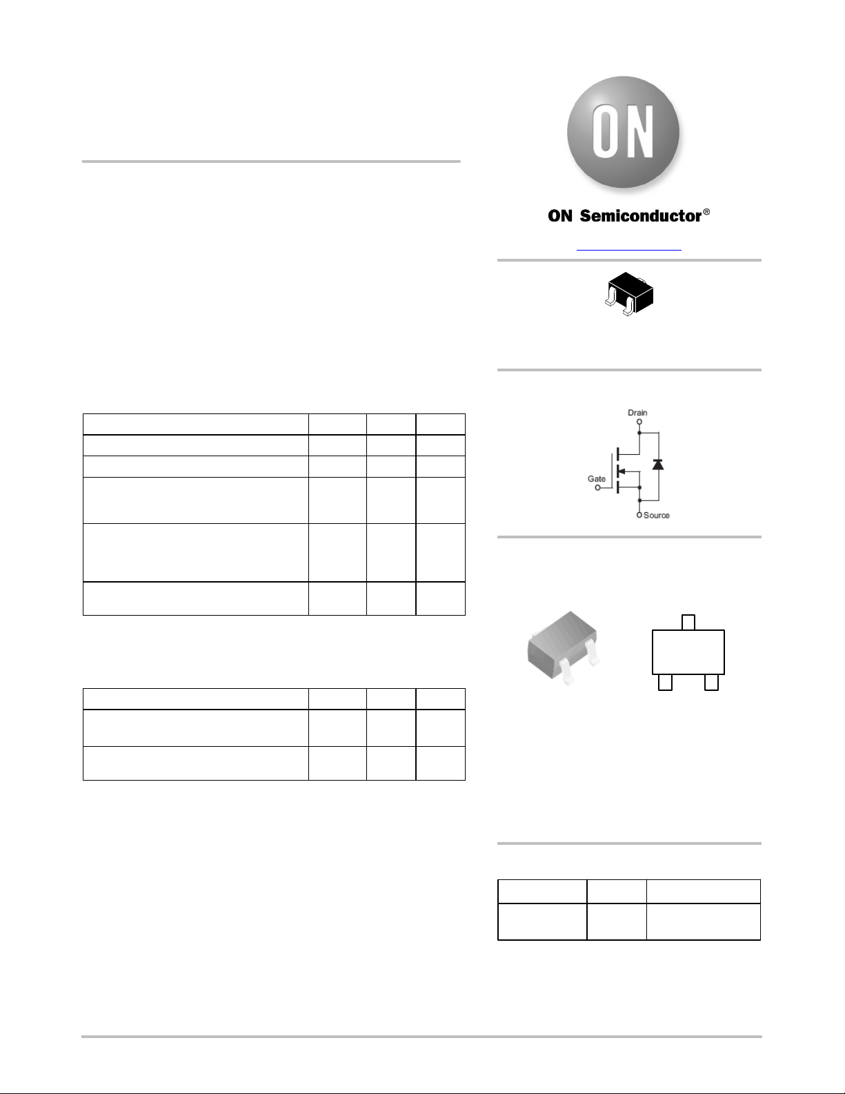
SC−70/SOT−323
CASE 419
SIMPLIFIED SCHEMATIC
MARKING DIAGRAM
& PIN ASSIGNMENT
Drain
3
D
&E&Y
S
G
Line 1:
&E = Space
&Y = Binary Year Code
Line 2:
&Z = Designates the Assembly Plant Code
2N = Specific Device Code
&G = 1−digit Week Code
&Z2N&G
21
Gate Source
© Semiconductor Components Industries, LLC, 2020
March, 2021 − Rev. 2
ORDERING INFORMATION
Device Package Shipping
2N7002W 3000 / Tape & Reel
†For information on tape and reel specifications,
including part orientation and tape sizes, please
refer to our Tape and Reel Packaging Specifications
Brochure, BRD8011/D.
1 Publication Order Number:
SC−70
(Pb−Free)
2N7002W−FCS/D
†
Page 2
2N7002W
ELECTRICAL CHARACTERISTICS (T
Parameter
= 25°C unless otherwise noted)
A
Symbol Test Condition Min Typ Max Units
OFF CHARACTERISTICS (Note 2)
Drain−Source Breakdown Voltage
Zero Gate Voltage Drain Current I
Gate−Body Leakage Current I
BV
DSS
DSS
GSS
VGS = 0 V, ID = 10 mA
VGS = 0 V,
V
= 60 V
DS
TC = 25°C 0.001 1.0 mA
TC = 125°C 7 500
VGS = ±20 V, VDS = 0 V 0.2 ±10 nA
60 78 V
ON CHARACTERISTICS (Note 2)
Gate Threshold Voltage
Static Drain−Source On−Resistance R
V
GS(th)
DS(ON)
VGS = VDS, ID = 250 mA
VGS = 5 V, ID = 0.05 A 1.6 7.5 W
1.0 1.76 2.0 V
VGS = 10 V, ID = 0.5 A, @ TJ = 125°C 2.53 13.5
On−State Drain Current I
Forward Transconductance g
D(ON)
FS
VGS = 10 V, VDS = 7.5 V 0.5 1.43 A
VDS = 10 V, ID = 0.2 A 80 356.5 mS
DYNAMIC CHARACTERISTICS
Input Capacitance
Output Capacitance C
Reverse Transfer Capacitance C
C
ISS
OSS
RSS
VGS = 0 V, VDS = 25 V, f = 1.0 MHz
37.8 50
12.4 25
6.5 7.0
pF
SWITCHING CHARACTERISTICS
Turn−On Delay Time
Turn−Off Delay Time t
t
D(ON)
D(OFF)
V
= 10 V, VDD = 30 V, ID = 0.2 A,
GEN
= 150 W, R
R
L
GEN
= 25 W
5.85 20
12.5 20
ns
Product parametric performance is indicated in the Electrical Characteristics for the listed test conditions, unless otherwise noted. Product
performance may not be indicated by the Electrical Characteristics if operated under different conditions.
2. Short duration test pulse used to minimize self−heating effect.
www.onsemi.com
2
Page 3

2N7002W
TYPICAL PERFORMANCE CHARACTERISTICS
1.6
= 10V
V
1.4
1.2
1.0
0.8
0.6
0.4
0.2
, DRAIN−SOURCE CURRENT (A)R
D
I
0.0
0
12345678910
GS
5V
4V
3V
2V
VDS, DRAIN−SOURCE VOLTAGE (V) ID, DRAIN−SOURCE CURRENT (A)
3.0
2.5
2.0
1.5
1.0
, DRAIN−SOURCE ON−RESISTANCE (W)
DS(on)
R
VGS = 3V
0.0 0.2 0.4 0.6 0.8 1.0
4V
4.5V
7V
5V
8V
6V
10V
9V
Figure 1. On−Region Characteristics Figure 2. On−Resistance Variation with Gate
Voltage and Drain Current
3.0
2.5
2.0
1.5
1.0
VGS = 10 V
I
= 500 mA
D
3.0
2.5
2.0
1.5
ID = 50 mA
= 500 mA
I
D
, DRAIN−SOURCE ON−RESISTANCE (W)
0.5
−50 0 50 100 150
DS(on)
TJ, JUNCTION TEMPERATURE (°C)
Figure 3. On−Resistance Variation with
Temperature
1.0
VDS = 10 V
0.8
0.6
0.4
0.2
, DRAIN−SOURCE CURRENT (A)
D
I
0.0
2
TJ = −25°C
25°C
125°C
75°C
3456
VGS, GATE−SOURCE VOLTAGE (V) TJ, JUNCTION TEMPERATURE (°C)
Figure 5. Transfer Characteristics Figure 6. Gate Threshold Variation with
150°C
1.0
, DRAIN−SOURCE ON−RESISTANCE (W)
210
DS(on)
R
468
VGS, GATE−SOURCE VOLTAGE (V)
Figure 4. On−Resistance Variation with
Gate−Source Voltage
2.5
VGS = V
DS
2.0
ID = 1 mA
1.5
1.0
−50 0 50 100 150
, GATE−SOURCE THRESHOLD VOLTAGE (V)
th
V
ID = 0.25 mA
Temperature
www.onsemi.com
3
Page 4

100
2N7002W
TYPICAL PERFORMANCE CHARACTERISTICS
280
= 0 V
V
GS
150°C
240
200
160
25°C
10
, REVERSE DRAIN CURRENT (mA)
S
I
1
0.0 0.2 0.4 0.6 0.8
VSD, BODY DIODE FORWARD VOLTAGE (V)
Figure 7. Reverse Drain Current Variation with
Diode Forward Voltage and Temperature
−55°C
1.0
120
80
, POWER DISSIPATION (mW)
40
C
P
0
0
25 50 75 100 125 150 175
TA, AMBIENT TEMPERATURE (°C)
Figure 8. Power Derating
www.onsemi.com
4
Page 5

MECHANICAL CASE OUTLINE
PACKAGE DIMENSIONS
SC−70, 3 Lead, 1.25x2
CASE 419AB−01
ISSUE O
DATE 19 DEC 2008
D
ee
TOP VIEW
q1
E1
A2
SYMBOL
A
A1
A2 0.80 1.00
b
c
E
D
E
E1
e
L
L1
L2
θ
θ1
A
q
MIN NOM MAX
0.80
0.00
0.15
0.08
1.80
1.80
1.15
0.26
0.90
2.00
2.10
1.25
0.65 BSC
0.36
0.42 REF
0.15 BSC
1.10
0.10
0.30
0.22
2.20
2.40
1.35
0.46
0º 8º
4º 10º
q1
SIDE VIEW END VIEW
Notes:
(1) All dimensions are in millimeters. Angles in degrees.
(2) Complies with JEDEC MO-203.
DOCUMENT NUMBER:
DESCRIPTION:
ON Semiconductor and are trademarks of Semiconductor Components Industries, LLC dba ON Semiconductor or its subsidiaries in the United States and/or other countries.
ON Semiconductor reserves the right to make changes without further notice to any products herein. ON Semiconductor makes no warranty, representation or guarantee regarding
the suitability of its products for any particular purpose, nor does ON Semiconductor assume any liability arising out of the application or use of any product or circuit, and specifically
disclaims any and all liability, including without limitation special, consequential or incidental damages. ON Semiconductor does not convey any license under its patent rights nor the
rights of others.
b
A1
98AON34256E
SC−70, 3 LEAD, 1.25X2
Electronic versions are uncontrolled except when accessed directly from the Document Repository.
Printed versions are uncontrolled except when stamped “CONTROLLED COPY” in red.
L
L1
L2
c
PAGE 1 OF 1
© Semiconductor Components Industries, LLC, 2019
www.onsemi.com
Page 6

ON Semiconductor and are trademarks of Semiconductor Components Industries, LLC dba ON Semiconductor or its subsidiaries in the United States and/or other countries.
ON Semiconductor owns the rights to a number of patents, trademarks, copyrights, trade secrets, and other intellectual property. A listing of ON Semiconductor’s product/patent
coverage may be accessed at www.onsemi.com/site/pdf/Patent−Marking.pdf
ON Semiconductor makes no warranty, representation or guarantee regarding the suitability of its products for any particular purpose, nor does ON Semiconductor assume any liability
arising out of the application or use of any product or circuit, and specifically disclaims any and all liability, including without limitation special, consequential or incidental damages.
Buyer is responsible for its products and applications using ON Semiconductor products, including compliance with all laws, regulations and safety requirements or standards,
regardless of any support or applications information provided by ON Semiconductor. “Typical” parameters which may be provided in ON Semiconductor data sheets and/or
specifications can and do vary in different applications and actual performance may vary over time. All operating parameters, including “Typicals” must be validated for each customer
application by customer’s technical experts. ON Semiconductor does not convey any license under its patent rights nor the rights of others. ON Semiconductor products are not
designed, intended, or authorized for use as a critical component in life support systems or any FDA Class 3 medical devices or medical devices with a same or similar classification
in a foreign jurisdiction or any devices intended for implantation in the human body. Should Buyer purchase or use ON Semiconductor products for any such unintended or unauthorized
application, Buyer shall indemnify and hold ON Semiconductor and its officers, employees, subsidiaries, affiliates, and distributors harmless against all claims, costs, damages, and
expenses, and reasonable attorney fees arising out of, directly or indirectly, any claim of personal injury or death associated with such unintended or unauthorized use, even if such
claim alleges that ON Semiconductor was negligent regarding the design or manufacture of the part. ON Semiconductor is an Equal Opportunity/Affirmative Action Employer. This
literature is subject to all applicable copyright laws and is not for resale in any manner.
. ON Semiconductor reserves the right to make changes without further notice to any products herein.
PUBLICATION ORDERING INFORMATION
LITERATURE FULFILLMENT:
Email Requests to: orderlit@onsemi.com
ON Semiconductor Website: www.onsemi.com
TECHNICAL SUPPORT
North American Technical Support:
Voice Mail: 1 800−282−9855 Toll Free USA/Canada
Phone: 011 421 33 790 2910
Europe, Middle East and Africa Technical Support:
Phone: 00421 33 790 2910
For additional information, please contact your local Sales Representative
◊
www.onsemi.com
1
 Loading...