

Page 1
1N5333B Series
Preferred Device
5 Watt Surmetict
40 Zener Voltage Regulators
This is a complete series of 5 Watt Zener diodes with tight limits and
better operating characteristics that reflect the superior capabilities of
silicon-oxide passivated junctions. All this in an axial lead,
transfer-molded plastic package that offers protection in all common
environmental conditions.
http://onsemi.com
Features
•Zener Voltage Range - 3.3 V to 200 V
•ESD Rating of Class 3 (>16 kV) per Human Body Model
•Surge Rating of up to 180 W @ 8.3 ms
•Maximum Limits Guaranteed on up to Six Electrical Parameters
•Pb-Free Packages are Available*
Mechanical Characteristics
CASE: Void free, transfer-molded, thermosetting plastic
FINISH: All external surfaces are corrosion resistant and leads are
readily solderable
MAXIMUM LEAD TEMPERATURE FOR SOLDERING PURPOSES:
260°C, 1/16 in. from the case for 10 seconds
POLARITY: Cathode indicated by polarity band
MOUNTING POSITION: Any
MAXIMUM RATINGS
Rating Symbol Value Unit
Max. Steady State Power Dissipation
= 75°C, Lead Length = 3/8 in
@ T
L
Derate above 75°C
Operating and Storage
Temperature Range
Stresses exceeding Maximum Ratings may damage the device. Maximum
Ratings are stress ratings only. Functional operation above the Recommended
Operating Conditions is not implied. Extended exposure to stresses above the
Recommended Operating Conditions may affect device reliability.
P
TJ, T
D
-65 to +200 °C
stg
40
5
W
mW/°C
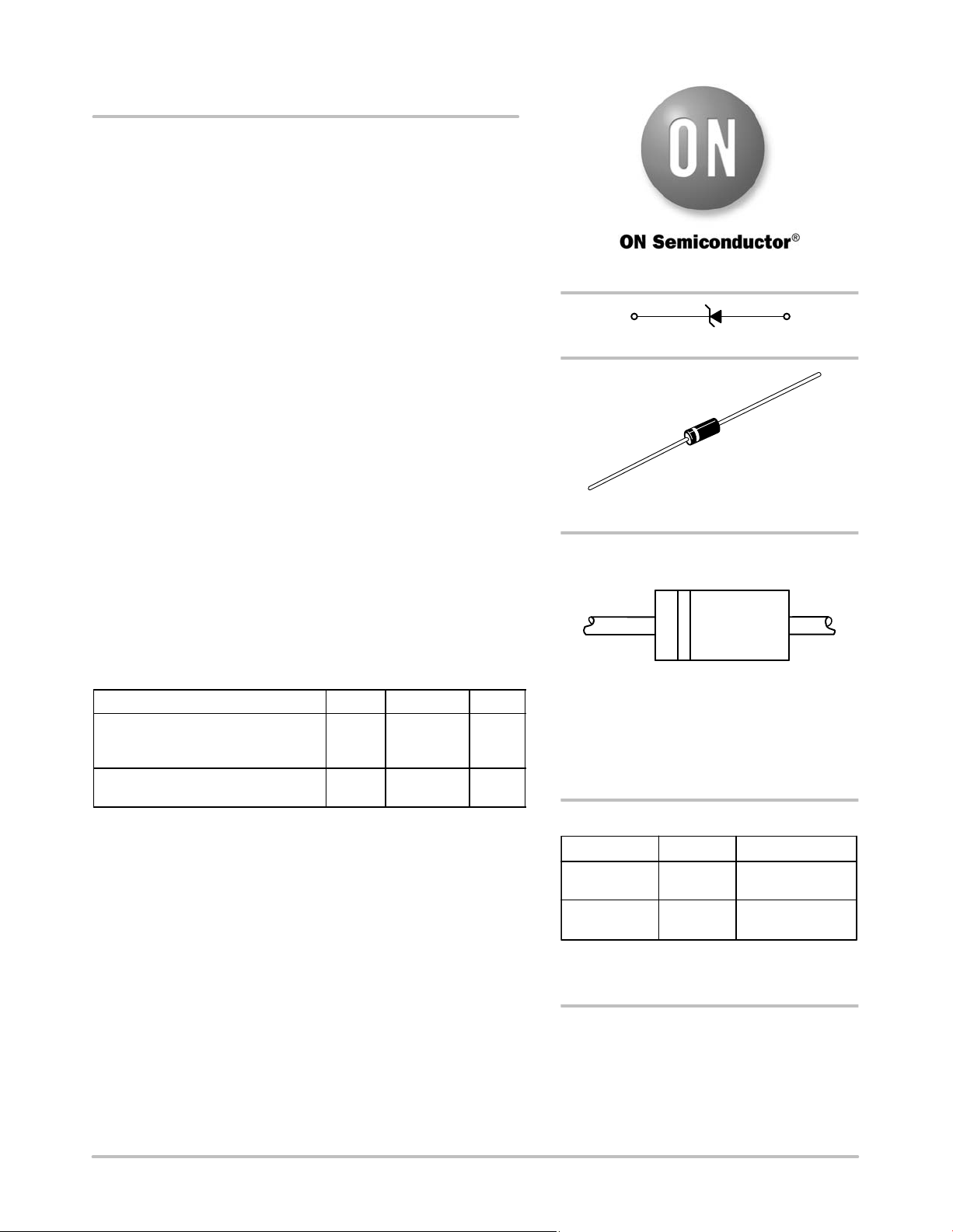
Cathode Anode
AXIAL LEAD
CASE 017AA
PLASTIC
MARKING DIAGRAM
A
1N
53xxB
YYWWG
G
A = Assembly Location
1N53xxB = Device Number
YY = Year
WW = Work Week
G = Pb-Free Package
(Note: Microdot may be in either location)
(Refer to Tables on Pages 3 & 4)
ORDERING INFORMATION
Device Package Shipping
1N53xxB, G Axial Lead
(Pb-Free)
1N53xxBRL, G Axial Lead
(Pb-Free)
†For information on tape and reel specifications,
including part orientation and tape sizes, please
refer to our Tape and Reel Packaging Specifications
Brochure, BRD8011/D.
Preferred devices are recommended choices for future use
and best overall value.
1000 Units/Box
4000/Tape & Reel
†
*For additional information on our Pb-Free strategy and soldering details, please
download the ON Semiconductor Soldering and Mounting Techniques
Reference Manual, SOLDERRM/D.
© Semiconductor Components Industries, LLC, 2008
January, 2008 - Rev. 10
1 Publication Order Number:
1N5333B/D
Page 2

1N5333B Series
ELECTRICAL CHARACTERISTICS (T
otherwise noted, V
Symbol
V
Z
I
ZT
Z
ZT
I
ZK
Z
ZK
I
R
V
R
I
F
V
F
I
R
DV
Z
I
ZM
= 1.2 V Max @ IF = 1.0 A for all types)
F
Parameter
Reverse Zener Voltage @ I
Reverse Current
Maximum Zener Impedance @ I
Reverse Current
Maximum Zener Impedance @ I
Reverse Leakage Current @ V
Breakdown Voltage
Forward Current
Forward Voltage @ I
F
Maximum Surge Current @ TA = 25°C
Reverse Zener Voltage Change
Maximum DC Zener Current
ELECTRICAL CHARACTERISTICS (T
= 25°C unless
A
ZT
ZT
ZK
R
VRV
Z
I
I
F
I
R
I
ZT
Zener Voltage Regulator
= 25°C unless otherwise noted, VF = 1.2 V Max @ IF = 1.0 A for all types)
A
V
V
F
Leakage
Current
IR @ V
mA Max
I
R
(Note 3)
R
DV
Z
(Note 4)
(Note 5)
Volts A Volts mA
Device
(Note 1)
Zener Voltage (Note 2) Zener Impedance (Note 2)
†
Device
Marking
VZ (Volts) @ IZTZZT @ IZTZZK @ IZKI
Min Nom Max mA
W W
ZK
mA
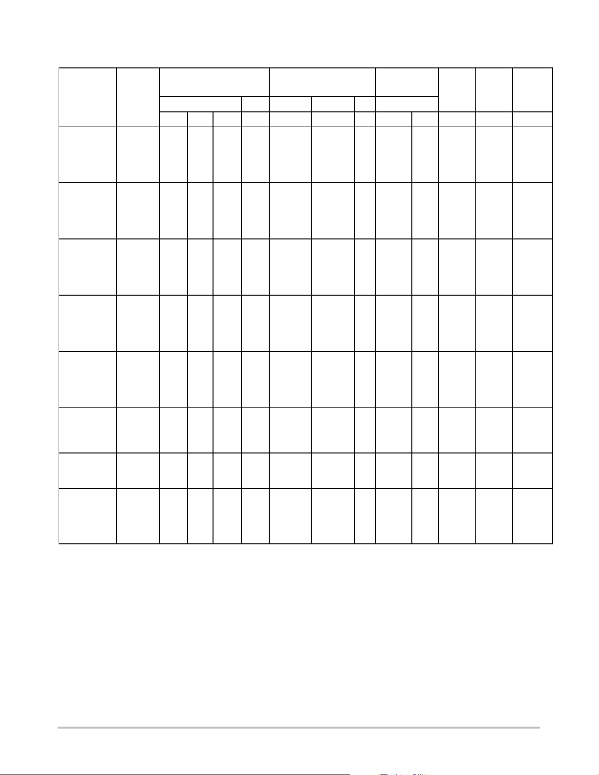
1N5333B, G 1N5333B 3.14 3.3 3.47 380 3 400 1 300 1 20 0.85 1440
1N5334BG 1N5334B 3.42 3.6 3.78 350 2.5 500 1 150 1 18.7 0.8 1320
1N5335BG 1N5335B 3.71 3.9 4.10 320 2 500 1 50 1 17.6 0.54 1220
1N5336BG 1N5336B 4.09 4.3 4.52 290 2 500 1 10 1 16.4 0.49 1100
1N5337BG 1N5337B 4.47 4.7 4.94 260 2 450 1 5 1 15.3 0.44 1010
1N5338BG 1N5338B 4.85 5.1 5.36 240 1.5 400 1 1 1 14.4 0.39 930
1N5339B, G 1N5339B 5.32 5.6 5.88 220 1 400 1 1 2 13.4 0.25 865
1N5340B, G 1N5340B 5.70 6.0 6.30 200 1 300 1 1 3 12.7 0.19 790
1N5341B, G 1N5341B 5.89 6.2 6.51 200 1 200 1 1 3 12.4 0.1 765
1N5342BG 1N5342B 6.46 6.8 7.14 175 1 200 1 10 5.2 11.5 0.15 700
1N5343BG 1N5343B 7.13 7.5 7.88 175 1.5 200 1 10 5.7 10.7 0.15 630
1N5344B, G 1N5344B 7.79 8.2 8.61 150 1.5 200 1 10 6.2 10 0.2 580
1N5345B, G 1N5345B 8.27 8.7 9.14 150 2 200 1 10 6.6 9.5 0.2 545
1N5346BG 1N5346B 8.65 9.1 9.56 150 2 150 1 7.5 6.9 9.2 0.22 520
1N5347B, G 1N5347B 9.50 10 10.5 125 2 125 1 5 7.6 8.6 0.22 475
Devices listed in bold, italic are ON Semiconductor Preferred devices. Preferred devices are recommended choices for future use and best overall value.
1. TOLERANCE AND TYPE NUMBER DESIGNATION: The JEDEC type numbers shown indicate a tolerance of ±5%.
2. ZENER VOLTAGE (V
40 ±10 ms prior to reading. Mounting contacts are located 3/8″ to 1/2″ from the inside edge of mounting clips to the body of the diode
= 25°C +8°C, -2°C).
(T
A
3. SURGE CURRENT (I
PW, of 8.3 ms. The data given in Figure 5 may be used to find the maximum surge current for a square wave of any pulse width between
) and IMPEDANCE (IZT and IZK): Test conditions for zener voltage and impedance are as follows: IZ is applied
Z
): Surge current is specified as the maximum allowable peak, non-recurrent square-wave current with a pulse width,
R
1 ms and 1000 ms by plotting the applicable points on logarithmic paper. Examples of this, using the 3.3 V and 200 V zener are shown in
Figure 6. Mounting contact located as specified in Note 2 (T
4. VOLTAGE REGULATION (DV
max value listed in the electrical characteristics table. The test current time duration for each VZ measurement is 40 ±10 ms. Mounting
of the I
Z
contact located as specified in Note 2 (T
5. MAXIMUM REGULATOR CURRENT (I
it applies only to the B-suffix device. The actual I
= 75°C at 3/8″ maximum from the device body.
T
L
): The conditions for voltage regulation are as follows: VZ measurements are made at 10% and then at 50%
Z
= 25°C +8°C, -2°C).
A
): The maximum current shown is based on the maximum voltage of a 5% type unit, therefore,
ZM
for any device may not exceed the value of 5 watts divided by the actual VZ of the device.
ZM
= 25°C +8°C, -2°C).
A
†The “G'' suffix indicates Pb-Free package or Pb-Free packages are available.
I
ZM
http://onsemi.com
2
Page 3
1N5333B Series
ELECTRICAL CHARACTERISTICS (T
= 25°C unless otherwise noted, VF = 1.2 V Max @ IF = 1.0 A for all types)
A
Leakage
Current
IR @ V
mA Max
I
R
(Note 8)
R
DV
Z
(Note 9)
I
ZM
(Note 10)
Volts A Volts mA
Device
(Note 6)
Zener Voltage (Note 7) Zener Impedance (Note 7)
†
Device
Marking
VZ (Volts) @ IZTZZT @ IZTZZK @ IZKI
Min Nom Max mA
W W
ZK
mA
1N5348BG 1N5348B 10.45 11 11.55 125 2.5 125 1 5 8.4 8.0 0.25 430
1N5349B, G 1N5349B 11.4 12 12.6 100 2.5 125 1 2 9.1 7.5 0.25 395
1N5350B, G 1N5350B 12.35 13 13.65 100 2.5 100 1 1 9.9 7.0 0.25 365
1N5351BG 1N5351B 13.3 14 14.7 100 2.5 75 1 1 10.6 6.7 0.25 340
1N5352B, G 1N5352B 14.25 15 15.75 75 2.5 75 1 1 11.5 6.3 0.25 315
1N5353B, G 1N5353B 15.2 16 16.8 75 2.5 75 1 1 12.2 6.0 0.3 295
1N5354B, G 1N5354B 16.15 17 17.85 70 2.5 75 1 0.5 12.9 5.8 0.35 280
1N5355B, G 1N5355B 17.1 18 18.9 65 2.5 75 1 0.5 13.7 5.5 0.4 264
1N5356BG 1N5356B 18.05 19 19.95 65 3 75 1 0.5 14.4 5.3 0.4 250
1N5357BG 1N5357B 19 20 21 65 3 75 1 0.5 15.2 5.1 0.4 237
1N5358B, G 1N5358B 20.9 22 23.1 50 3.5 75 1 0.5 16.7 4.7 0.45 216
1N5359B, G 1N5359B 22.8 24 25.2 50 3.5 100 1 0.5 18.2 4.4 0.55 198
1N5360BG 1N5360B 23.75 25 26.25 50 4 110 1 0.5 19 4.3 0.55 190
1N5361B, G 1N5361B 25.65 27 28.35 50 5 120 1 0.5 20.6 4.1 0.6 176
1N5362BG 1N5362B 26.6 28 29.4 50 6 130 1 0.5 21.2 3.9 0.6 170
1N5363BG 1N5363B 28.5 30 31.5 40 8 140 1 0.5 22.8 3.7 0.6 158
1N5364BG 1N5364B 31.35 33 34.65 40 10 150 1 0.5 25.1 3.5 0.6 144
1N5365B, G 1N5365B 34.2 36 37.8 30 11 160 1 0.5 27.4 3.5 0.65 132
1N5366B, G 1N5366B 37.05 39 40.95 30 14 170 1 0.5 29.7 3.1 0.65 122
1N5367BG 1N5367B 40.85 43 45.15 30 20 190 1 0.5 32.7 2.8 0.7 11 0
1N5368BG 1N5368B 44.65 47 49.35 25 25 210 1 0.5 35.8 2.7 0.8 100
1N5369B, G 1N5369B 48.45 51 53.55 25 27 230 1 0.5 38.8 2.5 0.9 93
1N5370B, G 1N5370B 53.2 56 58.8 20 35 280 1 0.5 42.6 2.3 1.0 86
1N5371BG 1N5371B 57 60 63 20 40 350 1 0.5 45.5 2.2 1.2 79
1N5372BG 1N5372B 58.9 62 65.1 20 42 400 1 0.5 47.1 2.1 1.35 76
1N5373B, G 1N5373B 64.6 68 71.4 20 44 500 1 0.5 51.7 2.0 1.52 70
1N5374BG 1N5374B 71.25 75 78.75 20 45 620 1 0.5 56 1.9 1.6 63
1N5375BG 1N5375B 77.9 82 86.1 15 65 720 1 0.5 62.2 1.8 1.8 58
1N5377BG 1N5377B 86.45 91 95.55 15 75 760 1 0.5 69.2 1.6 2.2 52.5
1N5378B, G 1N5378B 95 100 105 12 90 800 1 0.5 76 1.5 2.5 47.5
1N5380BG 1N5380B 114 120 126 10 170 1150 1 0.5 91.2 1.3 2.5 39.5
1N5381BG 1N5381B 123.5 130 136.5 10 190 1250 1 0.5 98.8 1.2 2.5 36.6
1N5383B, G 1N5383B 142.5 150 157.5 8 330 1500 1 0.5 114 1.1 3.0 31.6
1N5384BG 1N5384B 152 160 168 8 350 1650 1 0.5 122 1.1 3.0 29.4
1N5386BG 1N5386B 171 180 189 5 430 1750 1 0.5 137 1.0 4.0 26.4
1N5387BG 1N5387B 180.5 190 199.5 5 450 1850 1 0.5 144 0.9 5.0 25
1N5388B, G 1N5388B 190 200 210 5 480 1850 1 0.5 152 0.9 5.0 23.6
Devices listed in bold, italic are ON Semiconductor Preferred devices. Preferred devices are recommended choices for future use and best overall value.
6. TOLERANCE AND TYPE NUMBER DESIGNATION: The JEDEC type numbers shown indicate a tolerance of ±5%.
7. ZENER VOLTAGE (VZ) and IMPEDANCE (IZT and IZK): Test conditions for zener voltage and impedance are as follows: IZ is applied
40 ±10 ms prior to reading. Mounting contacts are located 3/8″ to 1/2″ from the inside edge of mounting clips to the body of the diode
= 25°C +8°C, -2°C).
(T
A
8. SURGE CURRENT (I
PW, of 8.3 ms. The data given in Figure 5 may be used to find the maximum surge current for a square wave of any pulse width between
): Surge current is specified as the maximum allowable peak, non-recurrent square-wave current with a pulse width,
R
1 ms and 1000 ms by plotting the applicable points on logarithmic paper. Examples of this, using the 3.3 V and 200 V zener are shown in
Figure 6. Mounting contact located as specified in Note 7 (T
9. VOLTAGE REGULATION (DV
max value listed in the electrical characteristics table. The test current time duration for each VZ measurement is 40 ±10 ms. Mounting
of the I
Z
contact located as specified in Note 7 (T
10.MAXIMUM REGULATOR CURRENT (I
it applies only to the B-suffix device. The actual I
= 75°C at 3/8″ maximum from the device body.
T
L
): The conditions for voltage regulation are as follows: VZ measurements are made at 10% and then at 50%
Z
= 25°C +8°C, -2°C).
A
): The maximum current shown is based on the maximum voltage of a 5% type unit, therefore,
ZM
for any device may not exceed the value of 5 watts divided by the actual VZ of the device.
ZM
= 25°C +8°C, -2°C).
A
†The “G'' suffix indicates Pb-Free package or Pb-Free packages are available.
http://onsemi.com
3
Page 4

°C/W)
1N5333B Series
40
30
20
L L
10
0
0 0.2 0.4 0.6 0.8 1
, JUNCTION‐TO‐LEAD THERMAL RESISTANCE (
JL
θ
L, LEAD LENGTH TO HEATSINK (INCH)
PRIMARY PATH OF
CONDUCTION IS THROUGH
THE CATHODE LEAD
Figure 1. Typical Thermal Resistance
TEMPERATURE COEFFICIENTS
10
8
6
ZT
4
2
(mV/°C) @ I
0
, TEMPERATURE COEFFICIENT
Z
-2
θ V
34 56
VZ, ZENER VOLTAGE @ IZT (VOLTS)
RANGE
7
8910
Figure 2. Temperature Coefficient‐Range for Units 3 to 10 Volts
300
200
100
ZT
50
30
20
(mV/°C) @ I
10
, TEMPERATURE COEFFICIENT
Z
5
θV
0 20 40 60 80 100 120 140 160 180 200 220
VZ, ZENER VOLTAGE @ IZT (VOLTS)
RANGE
Figure 3. Temperature Coefficient‐Range for Units 10 to 220 Volts
http://onsemi.com
4
Page 5

1N5333B Series
20
D = 0.5
10
C/W)
°
5
D = 0.2
D = 0.1
2
D = 0.05
1
D = 0.01
0.5
JUNCTION‐TO‐LEAD (
D = 0
0.2
(t, D), TRANSIENT THERMAL RESISTANCE
0.001 0.005 0.01 0.05 0.1 0.5 1 5 10 20 50 100
JL
θ
NOTE: BELOW 0.1 SECOND, THERMAL
NOTE: RESPONSE CURVE IS APPLICABLE
NOTE: TO ANY LEAD LENGTH (L).
t, TIME (SECONDS)
SINGLE PULSE D TJL = qJL(t)P
REPETITIVE PULSES D TJL = qJL(t, D)P
DUTY CYCLE, D = t1/t
Figure 4. Typical Thermal Response
L, Lead Length = 3/8 Inch
P
t
PK
1
2
PK
PK
t
2
40
20
10
4
2
1
0.4
, PEAK SURGE CURRENT (AMPS)
r
I
0.2
0.1
34 6810
*SQUARE WAVE
NOMINAL VZ (V)
PW=1ms*
PW=8.3ms*
PW=100ms*
PW=1000ms*
20 30 40 60 80 100 200
Figure 5. Maximum Non‐Repetitive Surge Current
versus Nominal Zener Voltage
(See Note 3)
T=25°C
1000
TC=25°C
30
20
10
5
2
1
0.5
, PEAK SURGE CURRENT (AMPS)
r
I
PLOTTED FROM INFORMATION
0.2
GIVEN IN FIGURE 5
0.1
1 10 100 1000
PW, PULSE WIDTH (ms)
VZ=3.3V
VZ=200V
Figure 6. Peak Surge Current versus Pulse Width
(See Note 3)
1000
T=25°C
100
100
10
, ZENER CURRENT (mA)
1
Z
I
0.1
1 234 5678 910
, ZENER VOLTAGE (VOLTS)
V
Z
Figure 7. Zener Voltage versus Zener Current
V
=3.3 thru 10 Volts
Z
10
, ZENER CURRENT (mA)
1
Z
I
0.1
10 20 30 40 50 60 70 80
http://onsemi.com
5
VZ, ZENER VOLTAGE (VOLTS)
Figure 8. Zener Voltage versus Zener Current
V
= 11 thru 75 Volts
Z
Page 6

1N5333B Series
100
10
, ZENER CURRENT (mA)
1
Z
I
0.1
80 100 120 140 160 180 200 220
, ZENER VOLTAGE (VOLTS)
V
Z
Figure 9. Zener Voltage versus Zener Current
V
= 82 thru 200 Volts
Z
APPLICATION NOTE
Since the actual voltage available from a given Zener
diode is temperature dependent, it is necessary to determine
junction temperature under any set of operating conditions
in order to calculate its value. The following procedure is
recommended:
Lead Temperature, T
, should be determined from:
L
TL = qLA PD + T
A
qLA is the lead‐to‐ambient thermal resistance and PD is the
power dissipation.
Junction Temperature, T
, may be found from:
J
TJ = TL + DT
JL
DTJL is the increase in junction temperature above the lead
temperature and may be found from Figure 4 for a train of
power pulses or from Figure 1 for dc power.
DTJL = qJL P
D
For worst‐case design, using expected limits of IZ, limits
and the extremes of TJ (DTJ) may be estimated.
of P
D
Changes in voltage, V
, can then be found from:
Z
DV = qVZ DT
J
qVZ, the Zener voltage temperature coefficient, is found
from Figures 2 and 3.
Under high power‐pulse operation, the Zener voltage will
vary with time and may also be affected significantly by the
zener resistance. For best regulation, keep current
excursions as low as possible.
Data of Figure 4 should not be used to compute surge
capability. Surge limitations are given in Figure 5. They are
lower than would be expected by considering only junction
temperature, as current crowding effects cause temperatures
to be extremely high in small spots resulting in device
degradation should the limits of Figure 5 be exceeded.
http://onsemi.com
6
Page 7

1N5333B Series
PACKAGE DIMENSIONS
SURMETIC 40, AXIAL LEAD
CASE 017AA-01
ISSUE O
NOTES:
1. CONTROLLING DIMENSION: INCH
2. LEAD DIAMETER AND FINISH NOT CONTROLLED
WITHIN DIMENSION F.
B
D
K
F
A
F
K
3. CATHODE BAND INDICATES POLARITY
DIM MIN MAX MIN MAX
A 0.330 0.350 8.38 8.89
B 0.130 0.145 3.30 3.68
D 0.037 0.043 0.94 1.09
F --- 0.050 --- 1.27
K 1.000 1.250 25.40 31.75
MILLIMETERSINCHES
SURMETIC is a trademark of Semiconductor Components Industries, LLC (SCILLC).
ON Semiconductor and are registered trademarks of Semiconductor Components Industries, LLC (SCILLC). SCILLC reserves the right to make changes without further notice
to any products herein. SCILLC makes no warranty, representation or guarantee regarding the suitability of its products for any particular purpose, nor does SCILLC assume any liability
arising out of the application or use of any product or circuit, and specifically disclaims any and all liability, including without limitation special, consequential or incidental damages.
“Typical” parameters which may be provided in SCILLC data sheets and/or specifications can and do vary in different applications and actual performance may vary over time. All
operating parameters, including “Typicals” must be validated for each customer application by customer's technical experts. SCILLC does not convey any license under its patent rights
nor the rights of others. SCILLC products are not designed, intended, or authorized for use as components in systems intended for surgical implant into the body, or other applications
intended to support or sustain life, or for any other application in which the failure of the SCILLC product could create a situation where personal injury or death may occur. Should
Buyer purchase or use SCILLC products for any such unintended or unauthorized application, Buyer shall indemnify and hold SCILLC and its officers, employees, subsidiaries, affiliates,
and distributors harmless against all claims, costs, damages, and expenses, and reasonable attorney fees arising out of, directly or indirectly, any claim of personal injury or death
associated with such unintended or unauthorized use, even if such claim alleges that SCILLC was negligent regarding the design or manufacture of the part. SCILLC is an Equal
Opportunity/Affirmative Action Employer. This literature is subject to all applicable copyright laws and is not for resale in any manner.
PUBLICATION ORDERING INFORMATION
LITERATURE FULFILLMENT:
Literature Distribution Center for ON Semiconductor
P.O. Box 5163, Denver, Colorado 80217 USA
Phone: 303-675-2175 or 800-344-3860 Toll Free USA/Canada
Fax: 303-675-2176 or 800-344-3867 Toll Free USA/Canada
Email: orderlit@onsemi.com
N. American Technical Support: 800-282-9855 Toll Free
USA/Canada
Europe, Middle East and Africa Technical Support:
Phone: 421 33 790 2910
Japan Customer Focus Center
Phone: 81-3-5773-3850
http://onsemi.com
ON Semiconductor Website: www.onsemi.com
Order Literature: http://www.onsemi.com/orderlit
For additional information, please contact your local
Sales Representative
1N5333B/D
7
 Loading...