ON Semiconducto NCV78702 User Manual
Multiphase Booster LED
Driver for Automotive Front
Lighting
NCV78702
The NCV78702 is a single−chip and high efficient booster for smart
Power ballast and LED Driver designed for automotive front lighting
applications like high beam, low beam, DRL (daytime running light),
turn indicator, fog light, static cornering, etc. The NCV78702 is in
particular designed for high current LEDs and with NCV78723 (dual
channel buck)/713 (single channel) provides a complete solution to
drive multiple LED strings of up−to 60 V. It includes a current−mode
voltage boost controller which also acts as an input filter with a
minimum of external components. The available output voltage can be
customized. Two devices NCV78702 can be combined and the booster
circuits can operate together to function as a multiphase booster
(2−phase, 3−phase, 4−phase) in order to further optimize the filtering
effect of the booster and lower the total application BOM cost for
higher power. Thanks to the SPI programmability, one single
hardware configuration can support various application platforms.
Features
• Single Chip
• Multiphase Booster
• High Overall Efficiency
• Minimum of External Components
• Active Input Filter with Low Current Ripple from Battery
• Integrated Boost Controller
• Programmable Input Current Limitation
• High Operating Frequencies to Reduce Inductor Sizes
• PCB Trace for Current Sense Shunt Resistor is Possible
• Low EMC Emission
• SPI Interface for Dynamic Control of System Parameters
• Fail Save Operating (FSO) Mode, Stand−Alone Mode
• Integrated Failure Diagnostic
www.onsemi.com
20
241
QFNW24
MW SUFFIX
CASE 484AA
MARKING DIAGRAMS
N702−x
ALYWG
G
N702 = Specific Device Code
A = Assembly Location
L = Wafer Lot
Y = Year
W = Work Week
G = Pb−Free Package
(Note: Microdot may be in either location)
ORDERING INFORMATION
See detailed ordering and shipping information on page 31 of
this data sheet.
1
TSSOP20
DE SUFFIX
CASE 948AB
N702−0
ALYWG
G
Typical Applications
• High Beam
• Low Beam
• DRL
• Position or Park Light
• Turn Indicator
• Fog
• Static Cornering
© Semiconductor Components Industries, LLC, 2016
January, 2021 − Rev. 3
1 Publication Order Number:
NCV78702/D
mC
V_Batt
(after rev . pol. prot.)
of MCU
V
CC
C_BC 1
R_SDO
C_BST _IN
C_BC 2
NCV78702
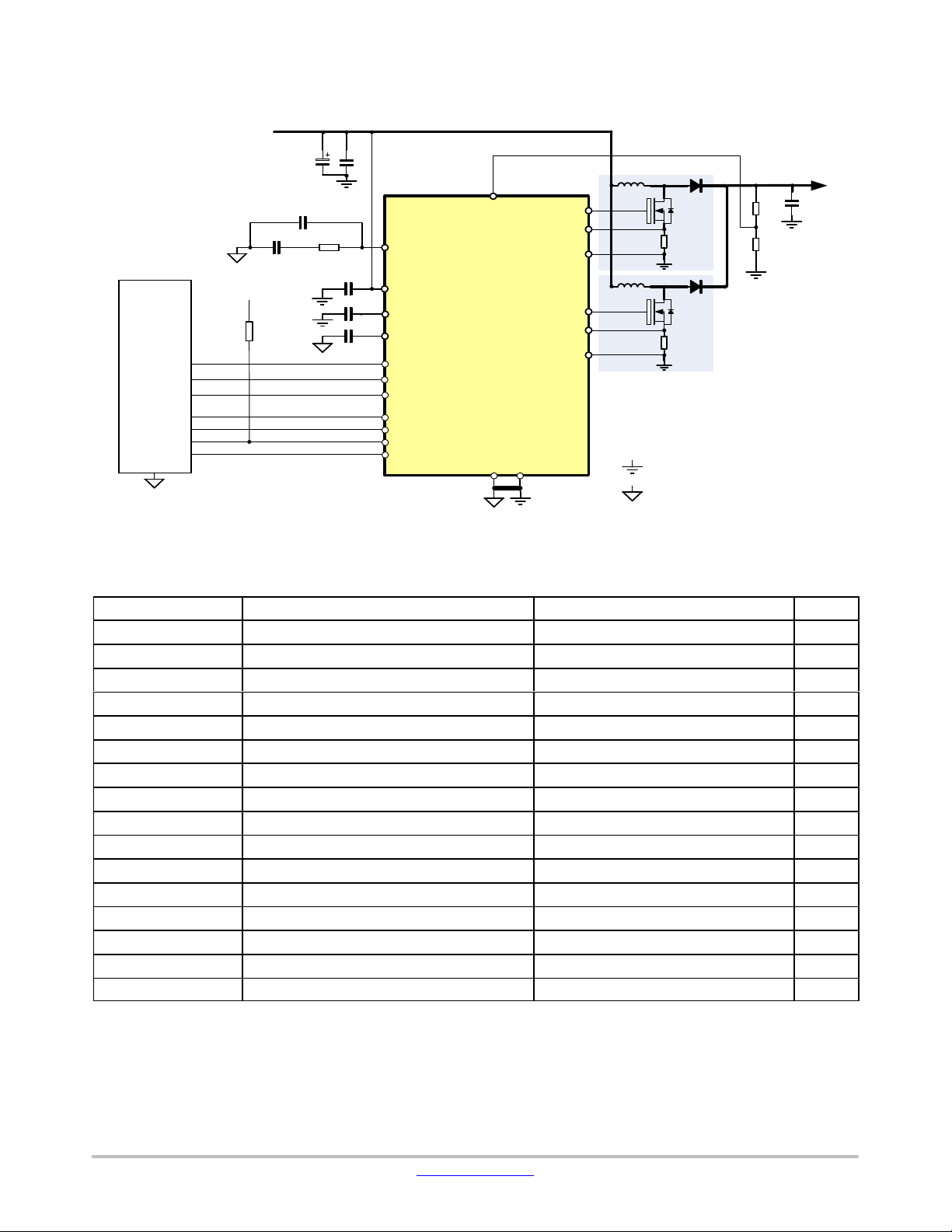
TYPICAL APPLICATION SCHEMATIC
R_BC 1
C_BB
C_VDRIVE
C_DD
COMP
ON Semiconductor
VBB
VDRIVE
VDD
ENABLE 1
BSTSYNC /TST /TST1
FSO/ ENABLE2
SPI_SCLK /TST 2
SPI_SDI
SPI_SDO
SPI_SCS
LED driver
2 phase booster
NCV78702
VBOOSTDIV
GND GNDP
VGATE 1
IBSTSENSE 1+
IBSTSENSE 1−
VGATE 2
IBSTSENSE 2+
IBSTSENSE 2−
L1
L2
PWR GND
Sig GND
T1
R_SENSE 1
Phase 1
T2
R_SENSE 2
Phase 2
D1
D2
RD1
RD2
Vboost
C_BST
Figure 1. Typical Application Schematic
Table 1. EXTERNAL COMPONENTS
Component Function Typ. Value Unit
L1, L2 Booster regulator coil 10
T1, T2 Booster regulator switching transistor e.g. NTD6416ANL
D1, D2 Booster regulator diode e.g. MBR5H100MFS
R_SENSE1, R_SENSE2 Booster regulator current sensing resistor 10
C_BST Booster regulator output capacitor 0.44
C_BB VBB decoupling capacitance (Note 1) 1
C_VDRIVE Capacitor for V
C_VDRIVE_ESR ESR of V
DRIVE
regulator 1
DRIVE
capacitor max. 200
C_DD VDD decoupling capacitor 1
C_DD_ESR ESR of VDD capacitor max. 200
R_SDO SPI pull−up resistor 1
C_BC1 Booster compensation network See Booster Compensator Model section
C_BC2 Booster compensation network See Booster Compensator Model section
R_BC1 Booster compensation network See Booster Compensator Model section
RD1 Booster output voltage feedback divider (Note 2) 107 (±1% tolerance)
RD2 Booster output voltage feedback divider (Note 2) 3.24 (±1% tolerance)
1. The value represents a potential initial startup value on a generic application. The actual size of the boost capacitor depends on the
application defined requirements (such as power level, operating ranges, number of phases) and transient performances with respect to the
rest of BOM. Please refer to application notes and tools provided by ON Semiconductor for further guidance. The chosen value must be
validated in the application.
2. Proposed values. Divider ratio (BSTDIV_RATIO) has to be 34. Tolerance of the resistors has to be ±1% to guarantee Booster parameters
(see Table 12).
mH
mW
mF/W
mF
mF
mW
mF
mW
kW
kW
kW
www.onsemi.com
2
VBB
VDRIVE
VDD
LDR
LDR
NCV78702
Booster
DIV
Vref
Error
VBOOSTDIV
amplifier
COMP
BSTSYNC ,
ENABLE 1,2,
TST 1/TST 2
SPI
Bandgap
POR
Bias
TSD
OSC
OTP
5V tolerant input
5V tolerant input /
OD output
Vref
Digital control
GND GNDP
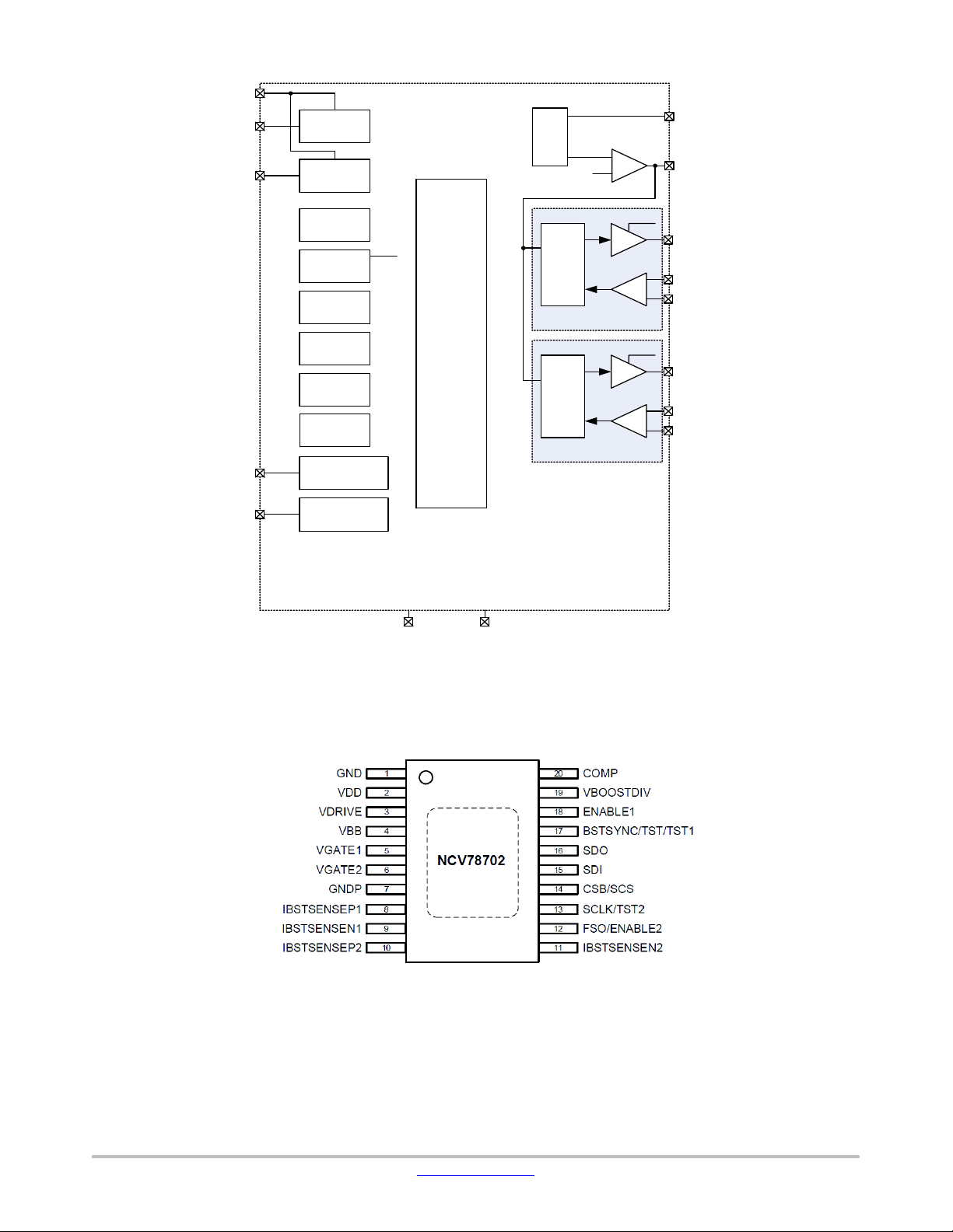
Figure 2. Block Diagram
PWM
PWM
Predriver
Current
sense CMP
Predriver
Current
sense CMP
Vdrive
VGATE 1
IBSTSENSE 1+
IBSTSENSE 1−
Vdrive
VGATE 2
IBSTSENSE 2+
IBSTSENSE 2−
PACKAGE AND PIN DESCRIPTION
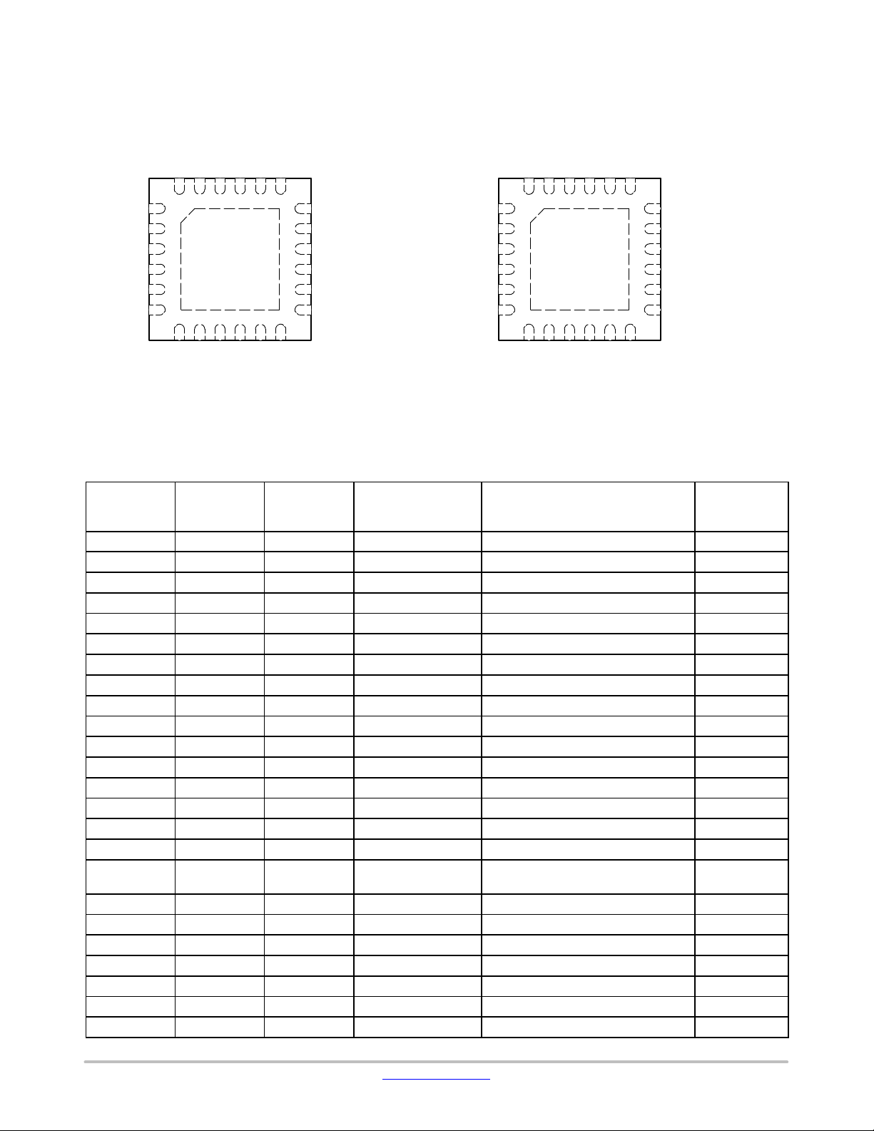
Figure 3. Pin Connections – QFNW24 4x4 0.5 and TSSOP−20 EP
www.onsemi.com
3
NC
VGATE1
VGATE2
NC
NC
NC
24
1
VBB
VDRIVE
VDD
NCV78702MW0A
GND
COMP
VBOOSTDIV
NCV78702
PACKAGE AND PIN DESCRIPTION
VDRIVENCVDD
24
1
ENABLE1
BSTSYNC/TST/TST1
SDO
SDI
CSB/SCS
SCLK/TST2
VBB
NC
VGATE1
NC
VGATE2
NC
GND
NCV78702MW1A
COMP
VBOOSTDIV
ENABLE1
BSTSYNC/TST/TST1
SDO
SDI
CSB/SCS
SCLK/TST2
GNDP
IBSTSENSE1+
IBSTSENSE1−
IBSTSENSE2+
IBSTSENSE2−
FSO/ENABLE2
GNDP
IBSTSENSE1+
IBSTSENSE1−
IBSTSENSE2+
IBSTSENSE2−
FSO/ENABLE2
Figure 3. Pin Connections – QFNW24 4x4 0.5 and TSSOP−20 EP
Table 2. PIN DESCRIPTION
Pin No.
QFNW24
MW0A
1 23 − NC NC NC
2 3 5 VGATE1 Booster MOSFET gate pre−driver MV out
3 5 6 VGATE2 Booster MOSFET gate pre−driver MV out
4 2 − NC NC NC
5 4 − NC NC NC
6 6 − NC NC NC
7 7 7 GNDP Power ground Ground
8 8 8 IBSTSENSE1+ Coil1 current positive feedback input MV in
9 9 9 IBSTSENSE1− Coil1 current negative feedback input MV in
10 10 10 IBSTSENSE2+ Coil2 current positive feedback input MV in
11 11 11 IBSTSENSE2− Coil2 current negative feedback input MV in
12 12 12 FSO/ENABLE2 FSO/ENABLE2 input MV in
13 13 13 SCLK/TST2 SPI clock / TST2 IO MV in
14 14 14 CSB/SCS SPI chip select (chip select bar) MV in
15 15 15 SDI SPI data input MV in
16 16 16 SDO SPI data output – pull up MV open−drain
17 17 17 BSTSYNC/TST/TST1 External clock for the boost regulator/
18 18 18 ENABLE1 ENABLE1 input MV in
19 19 19 VBOOSTDIV Booster high voltage feedback input HV in
20 20 20 COMP Compensation for the Boost regulator LV in/out
21 21 1 GND Ground Ground
22 22 2 VDD 3 V logic supply LV supply
23 24 3 VDRIVE 10 V supply MV supply
24 1 4 VBB Battery supply HV supply
Pin No.
QFNW24
MW1A
Pin No.
TSSOP−20 EP
Pin Name Description I/O Type
TM entry/ TST1 IO
HV in
www.onsemi.com
4
NCV78702
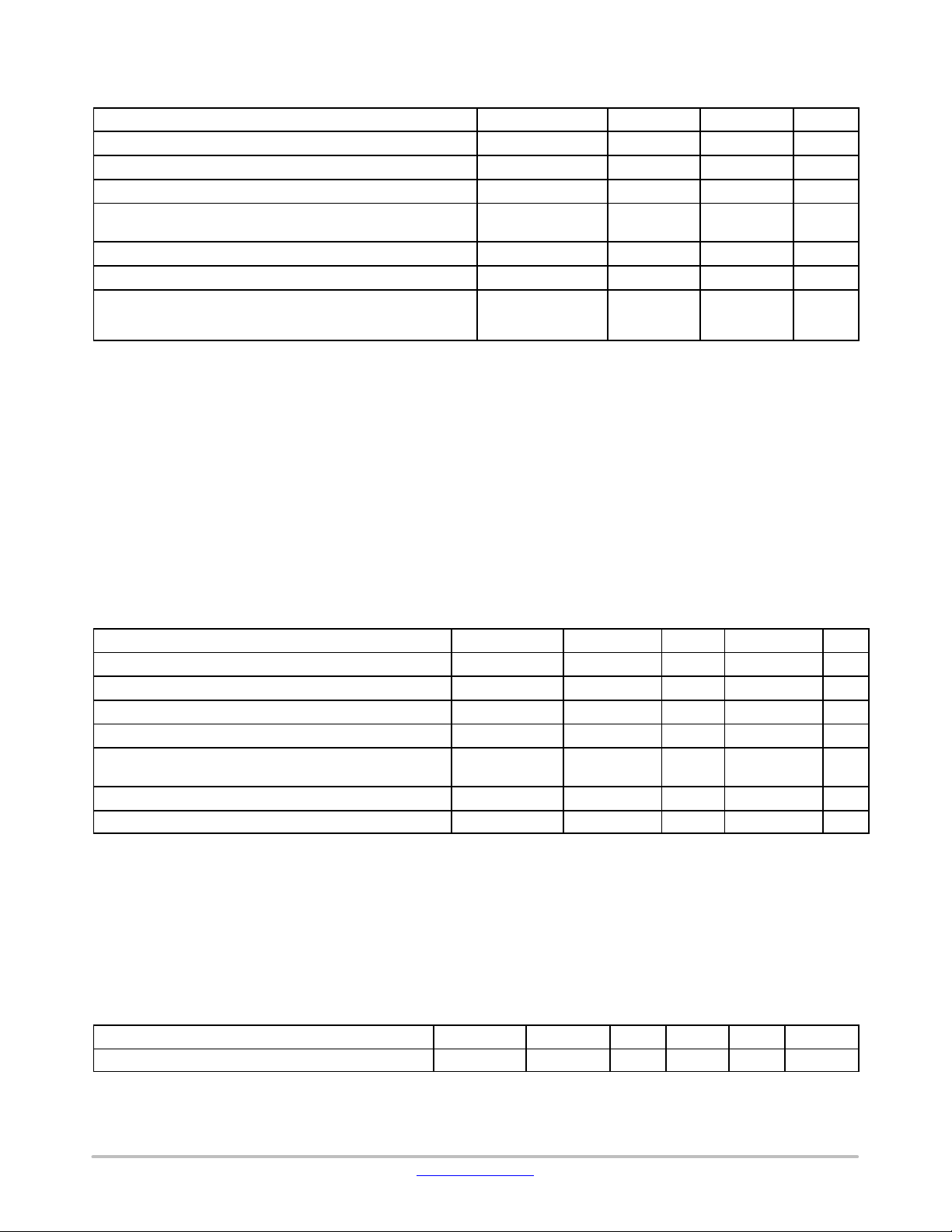
Table 3. ABSOLUTE MAXIMUM RATINGS
Characteristic Symbol Min Max Unit
Battery supply voltage (Note 4) V
Logic supply voltage (Note 5) V
Gate driver supply voltage (Note 6) V
Input current sense voltage (Note 7) IBSTSENSEPx,
Medium voltage IO pins (Note 8) IOMV −0.3 6.5 V
Storage Temperature (Note 9) T
Electrostatic Discharge on Component Level (Note 10)
Human Body Model
Charge Device Model
Stresses exceeding those listed in the Maximum Ratings table may damage the device. If any of these limits are exceeded, device functionality
should not be assumed, damage may occur and reliability may be affected.
3. Absolute maximum rating for VBB is 40 V for limited time < 0.5 s
4. Absolute maximum rating for pins: VBB, BSTSYNC/TST/TST1, VBOOSTDIV
5. Absolute maximum rating for pins: VDD, COMP
6. Absolute maximum rating for pins: VDRIVE, VGATE1, VGATE2
7. Absolute maximum rating for pins: IBSTSENSE1+, IBSTSENSE1−, IBSTSENSE2+, IBSTSENSE2−
8. Absolute maximum rating for pins: SCLK/TST2, CSB, SDI, SDO, ENABLE1, FSO/ENABLE2
9. For limited time up to 100 hours. Otherwise the max storage temperature is 85°C.
10.This device series incorporates ESD protection and is tested by the following methods:
ESD Human Body Model tested per EIA/JESD22−A114
ESD Charge Device Model tested per ESD−STM5.3.1−1999
Latch−up Current Maximum Rating: v100 mA per JEDEC standard: JESD78
BB
DD
DRIVE
IBSTSENSENx
STRG
V
ESD_HBM
V
ESD_CDM
−0.3 36 (Note 3) V
−0.3 3.6 V
−0.3 12 V
−1.0 12 V
−50 150 °C
−2
−500
+2
+500
kV
V
Operating ranges define the limits for functional
operation and parametric characteristics of the device. A
mission profile (Note 11) is a substantial part of the
operation conditions; hence the Customer must contact
ON Semiconductor in order to mutually agree in writing on
the allowed missions profile(s) in the application.
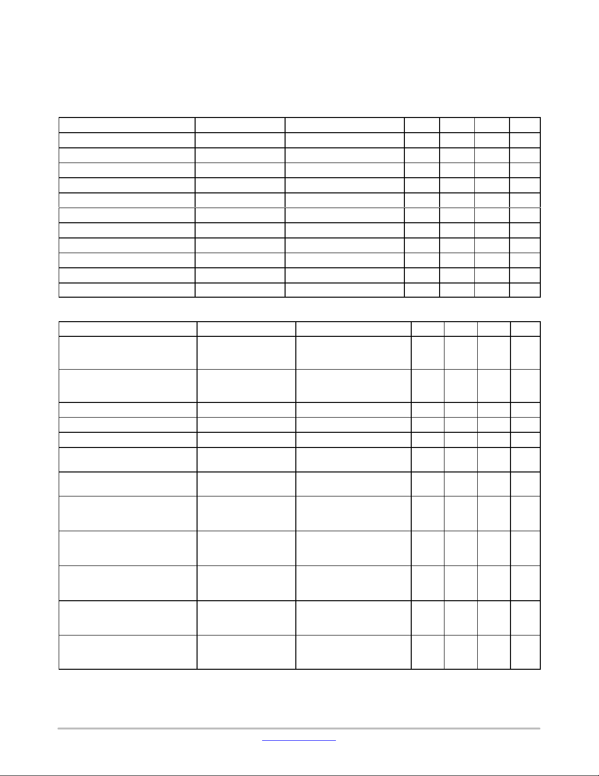
Table 4. RECOMMENDED OPERATING RANGES
Characteristic Symbol Min Ty p Max Unit
Battery supply voltage (Note 12 and 13) V
Logic supply voltage (Note 14) V
VDD current load I
Medium voltage IO pins IOMV 0 5 V
Input current sense voltage IBSTSENSEPx,
Functional operating junction temperature range (Note 15) T
Parametric operating junction temperature range (Note 16) T
Functional operation above the stresses listed in the Recommended Operating Ranges is not implied. Extended exposure to stresses beyond
the Recommended Operating Ranges limits may affect device reliability.
11. A mission profile describes the application specific conditions such as, but not limited to, the cumulative operating conditions over life time,
the system power dissipation, the system’s environmental conditions, the thermal design of the customer’s system, the modes, in which the
device is operated by the customer, etc. No more than 100 cumulated hours in life time above T
12.Minimum V
13.VDRIVE is supplied from VBB, it must be verified that VDRIVE voltage is appropriate for the external FETs.
14.VBB > 5 V
15.The circuit functionality is not guaranteed outside the functional operating junction temperature range. Also please note that the device is
verified on bench for operation up to 170°C but that the production test guarantees 155°C only.
16.The parametric characteristics of the circuit are not guaranteed outside the Parametric operating junction temperature range.
for OTP memory programming is 15.8 V.
BB
BB
DD
DD
IBSTSENSENx
JF
JP
5 30 V
3.1 3.5 V
50 mA
−0.1 1 V
−45 155 °C
−40 150 °C
.
tw
Table 5. THERMAL RESISTANCE
Characteristic Package Symbol Min Ty p Max Unit
Thermal Resistance Junction to Exposed Pad (Note 17) QFNW24 4x4 Rthjp 2.82 °C/W
17.Includes also typical solder thickness under the Exposed Pad (EP). Thermal resistance junction to PCB Top Layer.
www.onsemi.com
5
NCV78702
ELECTRICAL CHARACTERISTICS
Note: All Min and Max parameters are guaranteed over full battery voltage (5 V; 30 V) and junction temperature (T
JP
(−40°C; 150°C), unless otherwise specified.
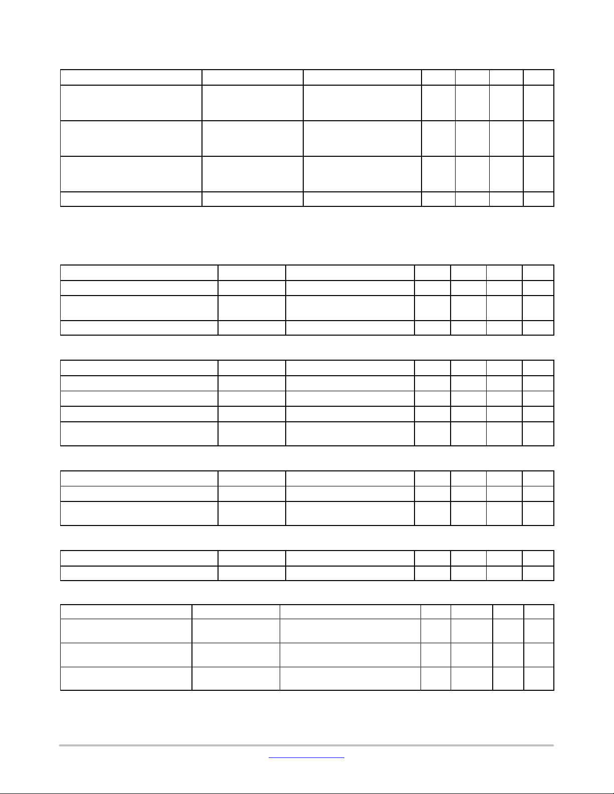
Table 6. TEMPERATURE MEASUREMENTS
Characteristic Symbol Conditions Min Typ Max Unit
Thermal Shutdown TSD 165 170 175 °C
Thermal Warning TW 155 160 165 °C
Thermal Output TEMP7 ADC_TEMP_THR[2:0] = 111 140 150 160 °C
Thermal Output TEMP6 ADC_TEMP_THR[2:0] = 110 130 140 150 °C
Thermal Output TEMP5 ADC_TEMP_THR[2:0] = 101 120 130 140 °C
Thermal Output TEMP4 ADC_TEMP_THR[2:0] = 100 110 120 130 °C
Thermal Output TEMP3 ADC_TEMP_THR[2:0] = 011 100 110 120 °C
Thermal Output TEMP2 ADC_TEMP_THR[2:0] = 010 90 100 110 °C
Thermal Output TEMP1 ADC_TEMP_THR[2:0] = 001 80 90 100 °C
Thermal Output TEMP0 ADC_TEMP_THR[2:0] = 000 70 80 90 °C
Thermal Output Hysteresis TEMP_HYST 3 °C
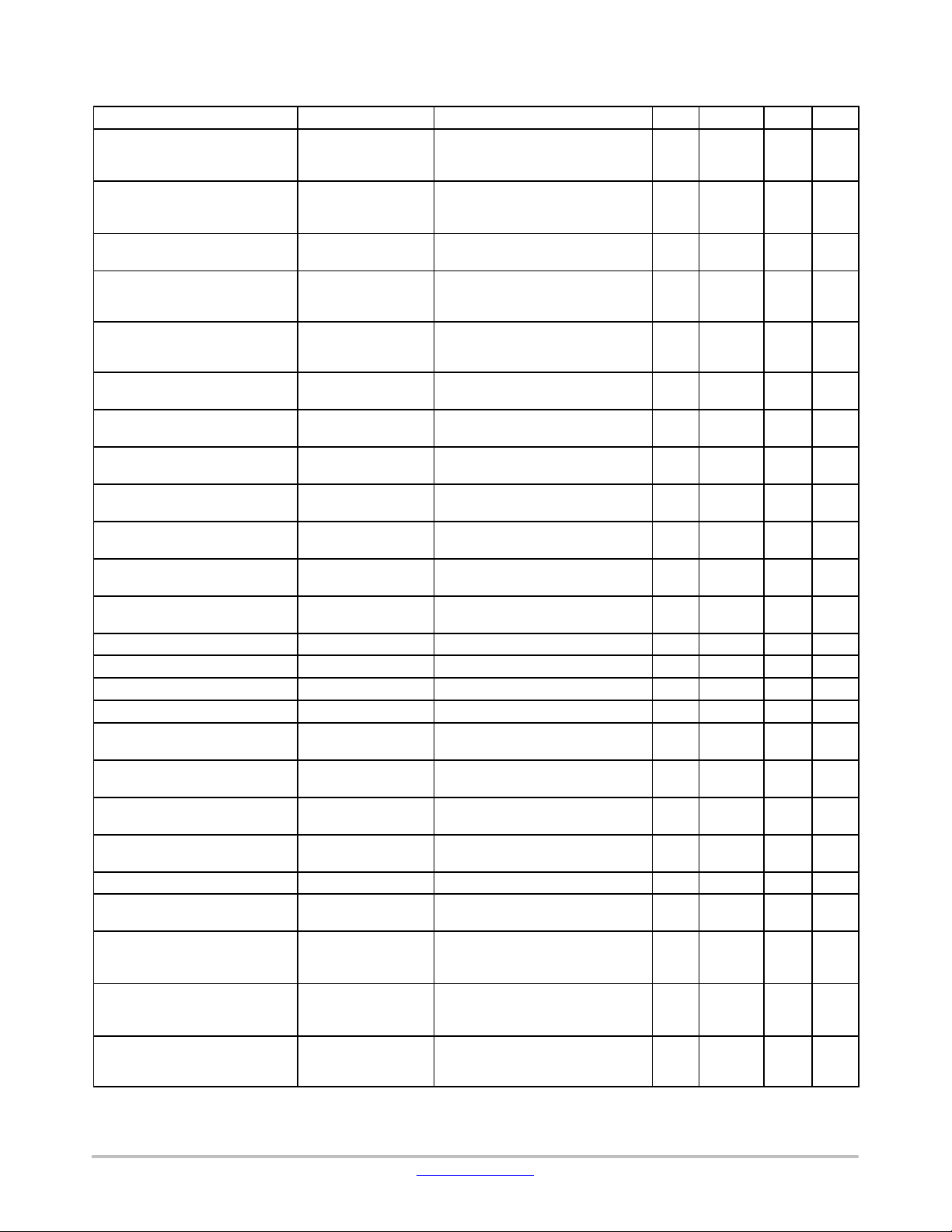
Table 7. VDRIVE: 10 V SUPPLY FOR BOOST FET GATE DRIVER CIRCUIT
Characteristic Symbol Conditions Min Ty p Max Unit
VDRIVE reg. voltage from VBB
(Note 18)
VDRIVE reg. voltage from VBB
(Note 18)
VDRIVE increase per code (Note 18)
DC output current consumption VDRV_ILIM 0 90 mA
Output current limitation VDRV_BB_IL 90 500 mA
Output overload condition for
VDRIVE_NOK detection (Note 19)
Minimum VBB−VDRIVE sufficient
voltage (Note 19)
VDRIVE UV detection threshold
(Note 20)
VDRIVE UV detection threshold
(Note 20)
VDRIVE UV detection threshold
(Note 20)
VDRIVE UV detection threshold
(Note 20)
VDRIVE UV detection threshold
(Note 20)
18.The VDRIVE voltage drop between VDRIVE and VBB has to be sufficient (min. 0.5 V).
19.Both of these conditions have to be fulfilled otherwise SPI status bit VDRIVE_NOK is set.
20.Relative threshold to typical value of VDRIVE_VSETPOINT settings.
VDRV_15 [VDRIVE_VSETPOINT =
VDRV_00 [VDRIVE_VSETPOINT =
DVDRV
VDRIVE_NOK_ILOAD 95 mA
VDRIVE_NOK_VBBLOW 0.5 V
VDRV_UV_[7] Relative threshold to actual
VDRV_UV_[6] Relative threshold to actual
VDRV_UV_[5] Relative threshold to actual
VDRV_UV_[4] Relative threshold to actual
VDRV_UV_[3] Relative threshold to actual
1111], Vbb − VDRIVE > 0.5 V
@IDRIVE = 90 mA
0000], Vbb − VDRIVE > 0.5
V @IDRIVE = 90 mA
Linear increase, 4 bits 0.34 V
VDRIVE_VSETPOINT
{VDRIVE_UV_THR = 111]
VDRIVE_VSETPOINT
{VDRIVE_UV_THR = 110]
VDRIVE_VSETPOINT
{VDRIVE_UV_THR = 101]
VDRIVE_VSETPOINT
{VDRIVE_UV_THR = 100]
VDRIVE_VSETPOINT
{VDRIVE_UV_THR = 011]
9.7 10.1 10.7 V
4.8 5 5.3 V
83 87 91 %
79 83 87 %
75 79 84 %
71 75 79 %
63 67 71 %
) range
www.onsemi.com
6
NCV78702
Table 7. VDRIVE: 10 V SUPPLY FOR BOOST FET GATE DRIVER CIRCUIT
Characteristic UnitMaxTypMinConditionsSymbol
VDRIVE UV detection threshold
(Note 20)
VDRIVE UV detection threshold
(Note 20)
VDRIVE UV detection threshold VDRV_UV_[0] Relative threshold to actual
VDRIVE UV detection delay VDRV_UV_DL 5 35
18.The VDRIVE voltage drop between VDRIVE and VBB has to be sufficient (min. 0.5 V).
19.Both of these conditions have to be fulfilled otherwise SPI status bit VDRIVE_NOK is set.
20.Relative threshold to typical value of VDRIVE_VSETPOINT settings.
Table 8. VDD: 3 V LOW VOLTAGE ANALOG AND DIGITAL SUPPLY
Characteristic Symbol Conditions Min Typ Max Unit
VDD regulator output voltage V
DC output current consumption VDD_IOUT Vbb > 5 V, including 10 mA self
Output current limitation VDD_ILIM 60 350 mA
VDRV_UV_[2] Relative threshold to actual
VDRV_UV_[1] Relative threshold to actual
DD
VDRIVE_VSETPOINT
{VDRIVE_UV_THR = 010]
VDRIVE_VSETPOINT
{VDRIVE_UV_THR = 001]
VDRIVE_VSETPOINT
{VDRIVE_UV_THR = 000]
Vbb > 5 V 3.135 3.465 V
current consumption
54 58 62 %
46 50 54 %
0 %
50 mA
ms
Table 9. POR: POWER−ON RESET CIRCUIT
Characteristic Symbol Conditions Min Typ Max Unit
POR Toggle level on VDD rising POR3V_H 2.55 3.05 V
POR Toggle level on VDD falling POR3V_L 2.3 2.8 V
POR Hysteresis POR3V_HYST 0.15 V
POR threshold on VBB, VBB rising POR_VBB_H Applicable only during startup
(VBB is rising)
3.8 4.3 V
Table 10. OTP MEMORY
Characteristic Symbol Conditions Min Typ Max Unit
Min. VBB for OTP zapping VBB_OTP 15.8 V
VBB range for OTP_FAIL flag during
OTP programming
VBB_OTP_L 13.2 14.1 15 V
Table 11. OSC10M: SYSTEM OSCILLATOR CLOCK
Characteristic Symbol Conditions Min Typ Max Unit
System oscillator frequency FOSC10M 7 10 13 MHz
Table 12. BOOSTER (Note 21)
Characteristic
Booster overvoltage shutdown BST_OV_127 [BOOST_OVERVOLTSD_THR
Booster overvoltage shutdown BST_OV_022 [BOOST_OVERVOLTSD_THR
Booster overvoltage shutdown
increase per code
21.All parameters are guaranteed for recommended external Vboost resistor divider (Rdiv) ratio 34 with ±1% tolerance.
22.Higher levels are valid if BST_VLIMTH value 2 or 3 (BOOST_VLIMTHx[1] = 1) is selected at least on one channel.
Symbol Conditions Min Typ Max Unit
63.8 65.85 67.9 V
11 11.5 12 V
DBST_OV
=1111111], DC level
=0010110], DC level
Linear increase, 7 bits 0.518 0.718 V
www.onsemi.com
7
NCV78702
Table 12. BOOSTER (Note 21)
Characteristic UnitMaxTypMinConditionsSymbol
Booster overvoltage
re−activation
Booster overvoltage
re−activation
Booster overvoltage re−activation decrease per code
Booster undervoltage protection
(external divider fail state detection)
Booster undervoltage protection
(external divider fail state detection) hysteresis
Booster regulation level BST_REG_125 [BOOST_VSETPOINT =1111101],
Booster regulation level BST_REG_022 [BOOST_VSETPOINT =0010110],
Booster regulation level increase
per code
Transconductance gain of Error
amplifier
Transconductance gain of Error
amplifier
Transconductance gain of Error
amplifier
Transconductance gain of Error
amplifier
EA max output current EA_IOUT_POS 150
EA min output current EA_IOUT_NEG −150
Output leakage current in tri−state EA_ILEAK Output in tri−state (EA_GM0) −1 1
EA output resistance EA_ROUT 2.0
EA max output voltage_3 COMP_CLH_3 BOOST_SLPCTRL[2]=1,
EA max output voltage_2 COMP_CLH_2 BOOST_SLPCTRL[2]=1,
EA max output voltage_1 COMP_CLH_1 BOOST_SLPCTRL[2]=0,
EA max output voltage_0 COMP_CLH_0 BOOST_SLPCTRL[2]=0,
EA min output voltage COMP_CLL 0.4 V
Booster VOOSTDIV pin input
pull up current
Division of COMP on the Current
comparator input
Division of COMP on the current
comparator input
Division of COMP on the current
comparator input
21.All parameters are guaranteed for recommended external Vboost resistor divider (Rdiv) ratio 34 with ±1% tolerance.
22.Higher levels are valid if BST_VLIMTH value 2 or 3 (BOOST_VLIMTHx[1] = 1) is selected at least on one channel.
BST_RA_3
BST_RA_0
DBST_RA
BST_EA_UV 3.45 3.95 4.45 V
BST_EA_UV_HYST 0.6 V
DBST_REG
BST_EA_GM3 [BOOST_OTA_GAIN =11], seen
BST_EA_GM2 [BOOST_OTA_GAIN =10], seen
BST_EA_GM1 [BOOST_OTA_GAIN =01], seen
BST_EA_GM0 [BOOST_OTA_GAIN =00],
BST_EA_DIV_INI Pull current source towards
COMP_DIV_15 [P_DISTRIBUTIONx =01111],
COMP_DIV_0 [P_DISTRIBUTIONx =00000],
COMP_DIV_−16 [P_DISTRIBUTIONx =11111],
[BOOST_OV_REACT =11], DV to
the Vboost reg. overvoltage protec-
tion, DC level
[BOOST_OV_REACT =00], DV to
the Vboost reg. overvoltage protec-
tion, DC level
Linear decrease, 2 bits, DC level −0.6 −0.5 V
DC level
DC level
Linear increase, 7 bits 0.518 0.718 V
from VBOOST, DC value
from VBOOST, DC value
from VBOOST, DC value
high impedance
OR of all BOOST_VLIMTHx[1]=1
OR of all BOOST_VLIMTHx[1]=0
OR of all BOOST_VLIMTHx[1]=1
OR of all BOOST_VLIMTHx[1]=0
to VDD voltage
signed, see Power Distribution sec-
tion and Table 19 for details
signed, see Power Distribution sec-
tion and Table 19 for details
signed, see Power Distribution sec-
tion and Table 19 for details
−1.9 −1.5 −1.1 V
0 V
62.8 64.8 66.8 V
10.8 11.5 12.2 V
63 90 117
42 60 78
21 30 39
0
2.1 2.26 V
1.98 V
1.64 V
1.35 V
0.4 0.8 1.4
20
6.81
4
mS
mS
mS
mS
mA
mA
mA
MW
mA
www.onsemi.com
8
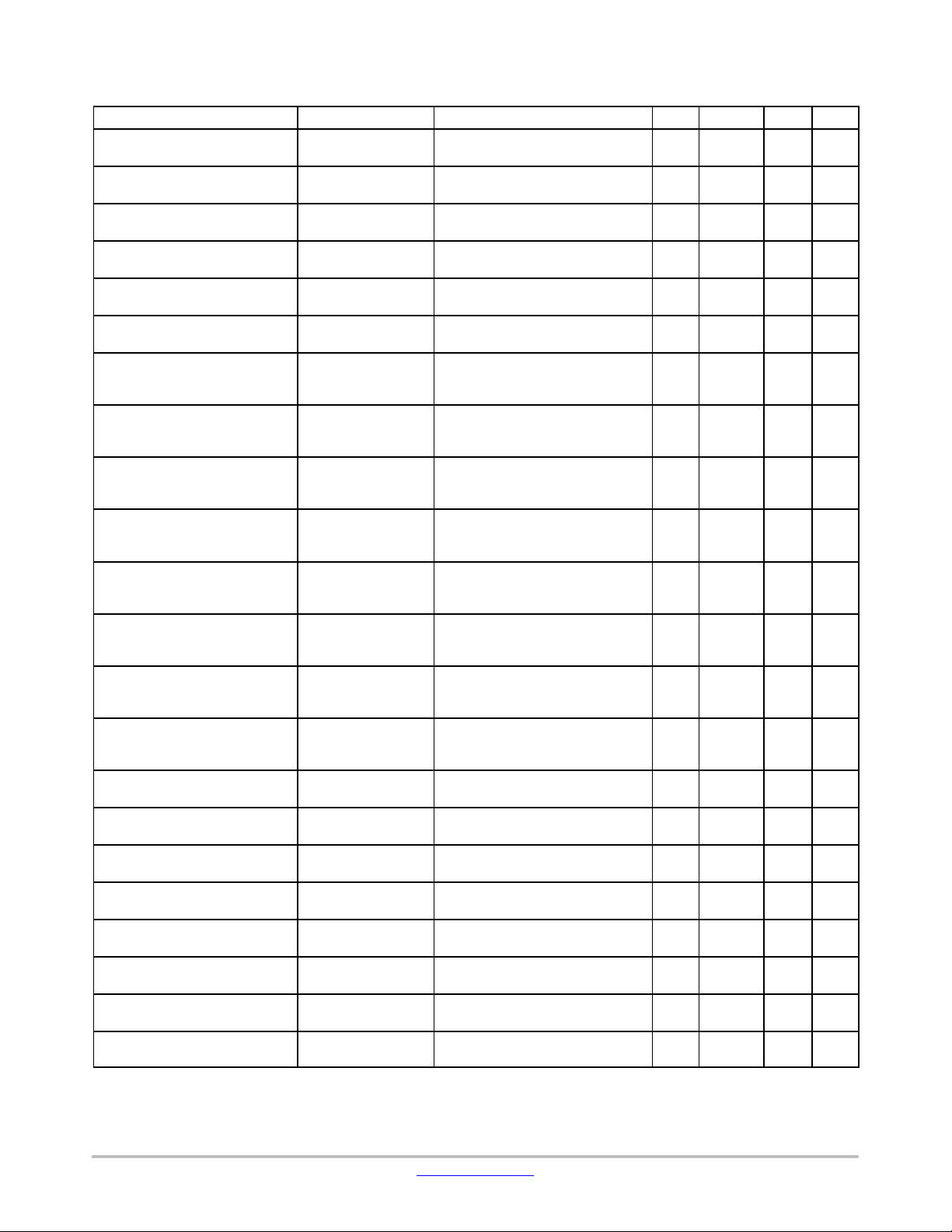
NCV78702
Table 12. BOOSTER (Note 21)
Characteristic UnitMaxTypMinConditionsSymbol
Voltage shift on COMP on Current comparator input
Booster skip cycle for low currents (Note 22)
Booster skip cycle for low currents (Note 22)
Booster skip cycle for low currents (Note 22)
VGATE comparator to start
BST_TOFF time
VGATE comparator to start
BST_TOFF time
Booster minimum OFF time BST_TOFF_7 [VBOOST_TOFF_SET = 111], time
Booster minimum OFF time BST_TOFF_6 VBOOST_TOFF_SET = 110], time
Booster minimum OFF time BST_TOFF_5 VBOOST_TOFF_SET = 101], time
Booster minimum OFF time BST_TOFF_4 VBOOST_TOFF_SET = 100], time
Booster minimum OFF time BST_TOFF_3 VBOOST_TOFF_SET = 011], time
Booster minimum OFF time BST_TOFF_2 VBOOST_TOFF_SET = 010], time
Booster minimum OFF time BST_TOFF_1 VBOOST_TOFF_SET = 001], time
Booster minimum OFF time BST_TOFF_0 VBOOST_TOFF_SET = 000], time
Booster minimum ON time BST_TON_7 [VBOOST_TON_SET =111], time
Booster minimum ON time BST_TON_6 [VBOOST_TON_SET =110], time
Booster minimum ON time BST_TON_5 [VBOOST_TON_SET =101], time
Booster minimum ON time BST_TON_4 [VBOOST_TON_SET =100], time
Booster minimum ON time BST_TON_3 [VBOOST_TON_SET =011], time
Booster minimum ON time BST_TON_2 [VBOOST_TON_SET =010], time
Booster minimum ON time BST_TON_1 [VBOOST_TON_SET =001], time
Booster minimum ON time BST_TON_0 [VBOOST_TON_SET =000], time
21.All parameters are guaranteed for recommended external Vboost resistor divider (Rdiv) ratio 34 with ±1% tolerance.
22.Higher levels are valid if BST_VLIMTH value 2 or 3 (BOOST_VLIMTHx[1] = 1) is selected at least on one channel.
COMP_VSF +0.5 V
BST_SKCL_3 [BOOST_SKCL =11], Booster dis-
abled for lower V(COMP)
BST_SKCL_2 [BOOST_SKCL =10], Booster dis-
abled for lower V(COMP)
BST_SKCL_1 [BOOST_SKCL =01], Booster dis-
abled for lower V(COMP)
BST_VGATE_THR_1 [VBOOST_VGATE_THR = 1] 1.2 V
BST_VGATE_THR_0 [VBOOST_VGATE_THR = 0] 0.4 V
780 1200 1620 ns
from VGATE below
VBOOST_VGATE_THR
300 460 620 ns
from VGATE below
VBOOST_VGATE_THR
260 400 540 ns
from VGATE below
VBOOST_VGATE_THR
220 340 460 ns
from VGATE below
VBOOST_VGATE_THR
180 280 380 ns
from VGATE below
VBOOST_VGATE_THR
140 220 300 ns
from VGATE below
VBOOST_VGATE_THR
100 160 220 ns
from VGATE below
VBOOST_VGATE_THR
from VGATE below
VBOOST_VGATE_THR
330 530 730 ns
from internal signal for VGATE drive
300 480 660 ns
from internal signal for VGATE drive
270 430 590 ns
from internal signal for VGATE drive
240 380 520 ns
from internal signal for VGATE drive
210 330 450 ns
from internal signal for VGATE drive
180 280 380 ns
from internal signal for VGATE drive
150 230 310 ns
from internal signal for VGATE drive
120 180 240 ns
from internal signal for VGATE drive
0.7/0.8 V
0.625/0.7 V
0.55/0.6 V
60 100 140 ns
www.onsemi.com
9
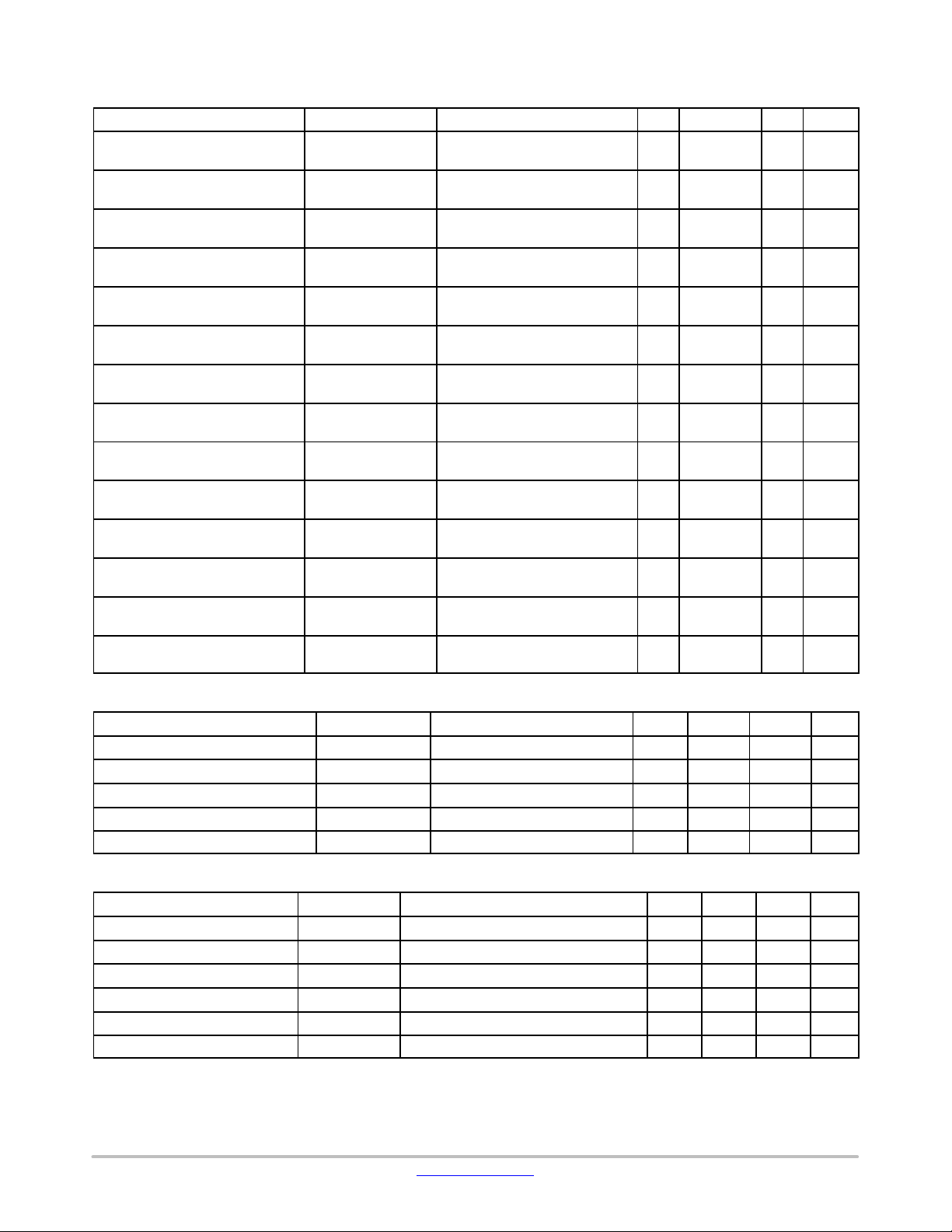
NCV78702
Table 13. BOOSTER – CURRENT REGULATION AND LIMITATION
Characteristic Symbol Conditions Min Ty p Max Unit
Current comparator for Imax detection
Current comparator for Imax detection
Current comparator for Imax detection
Current comparator for Imax detection
Current comparator for Vboost
regulation, offset voltage
Booster slope compensation BST_SLPCTRL_7 BOOST_SLPCTRL =111], see
Booster slope compensation BST_SLPCTRL_6 BOOST_SLPCTRL =110], see
Booster slope compensation BST_SLPCTRL_5 BOOST_SLPCTRL =101], see
Booster slope compensation BST_SLPCTRL_4 BOOST_SLPCTRL =100], see
Booster slope compensation BST_SLPCTRL_3 BOOST_SLPCTRL =011], see
Booster slope compensation BST_SLPCTRL_2 BOOST_SLPCTRL =010], see
Booster slope compensation BST_SLPCTRL_1 BOOST_SLPCTRL =001], see
Booster slope compensation BST_SLPCTRL_0 BOOST_SLPCTRL =000], see
Sense voltage common mode
range
BST_VLIMTHx_3 [BOOST_VLIMTHx =11], DC
level of threshold voltage
BST_VLIMTHx_2 [BOOST_VLIMTHx =10], DC
level of threshold voltage
BST_VLIMTHx_1 [BOOST_VLIMTHx =01], DC
level of threshold voltage
BST_VLIMTHx_0 [BOOST_VLIMTHx =00], DC
level of threshold voltage
BST_OFFS −10 10 mV
Power Distribution section
Power Distribution section
Power Distribution section
Power Distribution section
Power Distribution section
Power Distribution section
Power Distribution section
Power Distribution section
CMVSENSE Over full operating range −0.1 1 V
95 100 105 mV
75 80 85 mV
57 62.5 67 mV
45 50 55 mV
290 /
COMP_DIV
190 /
COMP_DIV
120 /
COMP_DIV
85 /
COMP_DIV
50 /
COMP_DIV
35 /
COMP_DIV
17 /
COMP_DIV
0
mV/ ms
mV/ ms
mV/ ms
mV/ ms
mV/ ms
mV/ ms
mV/ ms
mV/ ms
Table 14. BOOSTER – PRE−DRIVER
Characteristic Symbol Conditions Min Typ Max Unit
High−side switch impedance RONHI t = 25°C 4.2
High−side switch impedance RONHI t = 150°C 6 7
Low−side switch impedance RONLO t = 25°C 4.2
Low−side switch impedance RONLO t = 150°C 6 7
Pull down resistor on VGATEx RPDOWN 10
W
W
W
W
kW
Table 15. 5 V TOLERANT DIGITAL INPUTS (SCLK/TST2, CSB, SDI, BSTSYNC/TST/TST1, ENABLE1, FSO/ENABLE2)
Characteristic Symbol Conditions Min Typ Max Unit
High−level input voltage VINHI SDI, BSTSYNC, CSB and SCLK/TST2 2 V
Low−level input voltage VINLO SDI, BSTSYNC, CSB and SCLK/TST2 0.8 V
Pull resistance (Note 23) Rpull SDI, BSTSYNC, CSB and SCLK/TST2 40 160
High−level input voltage ENA_VINHI ENABLE1 and FSO/ENABLE2 2.35 V
Low−level input voltage ENA_VINLO ENABLE1 and FSO/ENABLE2 0.7 V
Pull resistance (Notes 23 and 24) ENA_Rpull ENABLE1 and FSO/ENABLE2 20 400
23.Internal pull down resistor (Rpd) for SDI, ENABLE1, FSO/ENABLE2, BSTSYNC and SCLK/TST2, pull up resistor (Rpu) for CSB to VDD.
24.VDD > POR3V_H; ENA_Rpull > 20 kW when VDD = 0 V to 3.5 V
kW
kW
www.onsemi.com
10
NCV78702
t
Table 16. 5 V TOLERANT OPEN−DRAIN DIGITAL OUTPUT (SDO)
Characteristic Symbol Conditions Min Typ Max Unit
Low−voltage output voltage VOUTLO Iout = −10 mA (current flows into the pin) 0.4 V
Equivalent output resistance RDSON Lowside switch 20 40
SDO pin leakage current SDO_ILEAK 2
SDO pin capacitance (Note 25) SDO_C 10 pF
CLK to SDO propagation delay SDO_DL Low−side switch activation/deactivation time;
@1 kW to 5 V, 100 pF to GND, for falling
edge V(SDO) goes below 0.5 V
25.Guaranteed by bench measurement, not tested in production.
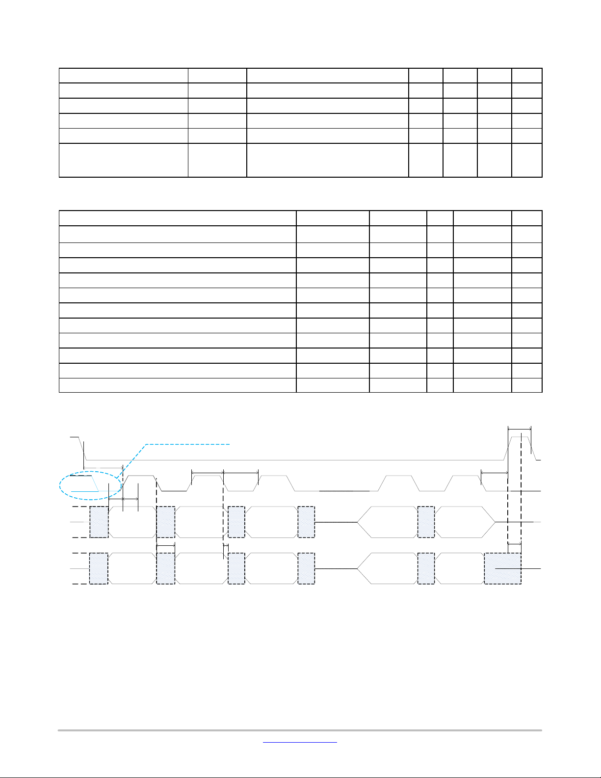
Table 17. SPI INTERFACE
Characteristic Symbol Min Typ Max Unit
CSB setup time
CSB hold time t
SCLK low time t
SCLK high time t
Data−in (DIN) setup time, valid data before rising edge of CLK t
Data−in (DIN) hold time, hold data after rising edge of CLK t
Output (DOUT) disable time (Note 26) t
Output (DOUT) valid (Note 26)
Output (DOUT) valid (Note 27)
Output (DOUT) hold time (Note 26) t
CSB high time t
26.SDO low–side switch activation time
27.Time depends on the SDO load and pull–up resistor
t
CSS
CSH
WL
WH
SU
DIS
t
V1→0
t
V0→1
HO
CS
H
0.5
0.25
0.5
0.5
0.25
0.275
0.07 0.32
0.07
1
60 ns
0.32
0.32 + t(RC)
W
mA
ms
ms
ms
ms
ms
ms
ms
ms
ms
ms
ms
V
V
V
V
V
V
V
V
IH
CSB
IL
IH
SCLK
IL
IH
DIN
IL
IH
DOUT
IL
HI−Z
Initial state of SCLK after CSB falling
edge is don’t care , it can be low or high
t
CSS
tSUt
H
DIN 15
t
V
DOUT 15 DOUT 14 DOUT 13 DOUT1 DOUT 0
DIN14
t
WH
t
WL
DIN 13
t
HO
DIN1 DIN 0
Figure 4. SPI Communication Timing
CS
t
CSH
t
DIS
HI−Z
www.onsemi.com
11
 Loading...