Current Sense Amplifier,
80V Common-Mode
Voltage, Unidirectional
Product Preview
NCS7030, NCS7031,
NCV7030, NCV7031
www.onsemi.com
The NCS7030 and NCS7031 are high voltage, current sense
amplifiers. They are available with gain options of 14 V/V and 20
V/V, with a maximum ±0.3 % gain error over the entire temperature
range. Each part consists of a preamplifier and buffer with access to
output and input via A1 and A2 pins for an intermediate filter network
or modified gain. The current sense amplifiers offer excellent input
common−mode rejection from −5 V to 80 V. They can perform
unidirectional current measurements across a sense resistor in a
variety of applications. Automotive qualified options are available
under NCV prefix. All versions are specified over the extended
operating temperature range from −40°C to 125°C.
Features
• Bandwidth: 100 kHz
• Input Offset Voltage: ±300 mV Max Over Temp
• Offset Drift over Temperature: ±3 mV/°C max
• Gain Error: ±0.3 % Max Over Temp
• Quiescent Current: 3 mA Typ
• Supply Voltage: 4.5 V to 5.5 V
• Common−Mode Input Voltage Range: −5 V to 80 V Operating,
−14 V to 85 V Survival
• CMRR: 90 dB Min
• PSRR: 70 dB Min
• Low−Pass Filter (1−pole or 2−pole)
• These are Pb−free Devices
Typical Applications
• Telecom Equipment
• Power Supply Designs
• Diesel Injection Control
• Automotive
• Motor Control
This document contains information on a product under development. ON Semiconductor
reserves the right to change or discontinue this product without notice.
8
1
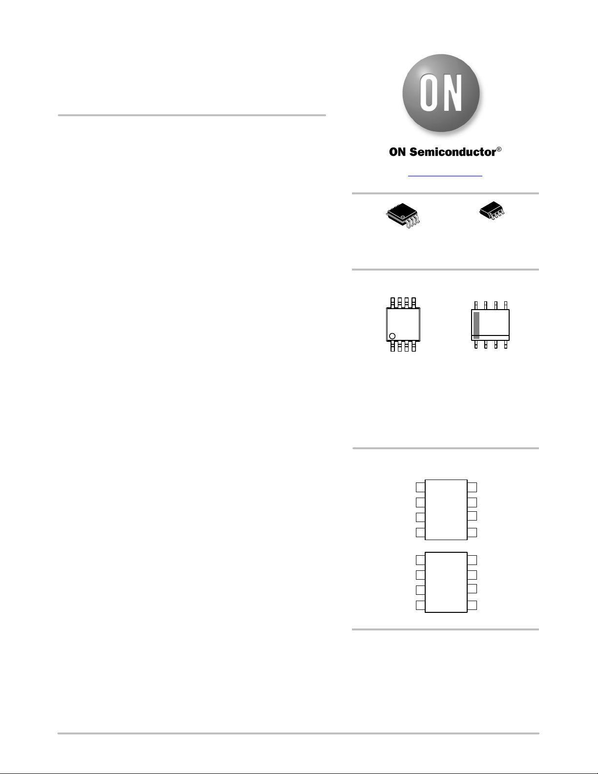
Micro8
CASE 846A−02
MARKING DIAGRAM
8
XXXX
AYW G
G
1
XXXXX = Specific Device Code
A = Assembly Location
L = Wafer Lot
Y = Year
W = Work Week
G = Pb−Free Package
(Note: Microdot may be in either location)
PIN CONNECTIONS
1
−IN
GND
2
NCS7031
3
4
1
2
NCS7030
3
4
G = 20
G = 14
A1
A2 OUT
−IN
GND
A1
A2 OUT
SOIC−8 NB
CASE 751−07
8
XXXXX
ALYWX
G
1
+IN
8
NC
7
V
6
S
5
8
+IN
V
7
S
NC
6
5
© Semiconductor Components Industries, LLC, 2015
October, 2020 − Rev. P5
ORDERING INFORMATION
See detailed ordering and shipping information on page 10 of
this data sheet.
1 Publication Order Number:
NCS7030/D

NCS7030, NCS7031, NCV7030, NCV7031
+IN
−IN
high−side
switch
EMI Filter
5 V
load
200 kW
V
S
NCS703x
200 kW
EMI Filter
+
−
V
S
or
G = x7
A1 A2
100 kW
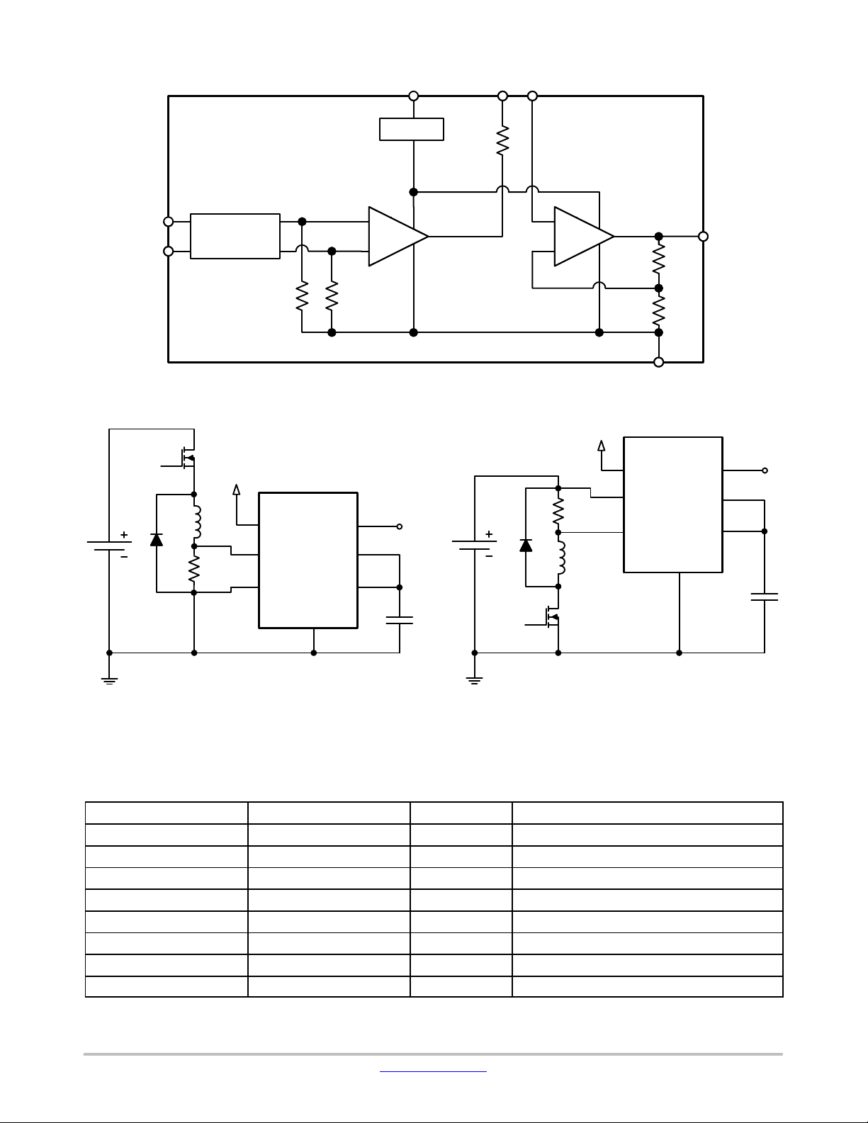
Figure 1. Simplified Block Diagram
OUT
+
−G = x10
sense
resistor
5 V
G = x2
10 kW
10 kW
+IN
−IN
GND
NCS703x
V
S
OUT
OUT
A1
A2
sense
resistor
Low−Side Current Sensing High−Side Current Sensing
+IN
−IN
GND
A1
A2
load
low−side
switch
Figure 2. Application Schematic
PIN FUNCTION DESCRIPTION
NCS7031 (G = 20) Pinout NCS7030 (G = 14) Pinout Pin Name Description
1 1 −IN Inverting input – connect to sense resistor
2 2 GND Device ground
3 3 A1 Pre−amp output connection
4 4 A2 Buffer amp input connection
5 5 OUT Device output
6 7 V
7 6 NC No connect
8 8 +IN Non−inverting input – connect to sense resistor
S
Power supply connection
GND
www.onsemi.com
2

NCS7030, NCS7031, NCV7030, NCV7031
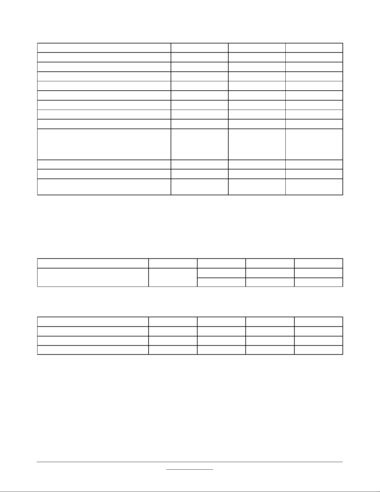
ABSOLUTE MAXIMUM RATINGS
Rating Symbol Value Unit
Supply Voltage Range (Note 1) V
Input Common−Mode Range V
Differential Input Voltage V
Maximum Input Current I
Maximum Output Current I
Continuous Total Power Dissipation P
Maximum Junction Temperature T
Storage Temperature Range T
S
CM
ID
I
O
D
J(max)
STG
ESD Capability (Note 2)
Human Body Model, Input pins
Human Body Model, All other pins
Charged Device Model
HBM
HBM
CDM
Latch−Up Current (Note 3) ±100 mA
Moisture Sensitivity Level MSL Level 1 −
Lead Temperature Soldering
T
SLD
Reflow (SMD Styles Only), Pb−Free Versions (Note 4)
Stresses exceeding those listed in the Maximum Ratings table may damage the device. If any of these limits are exceeded, device functionality
should not be assumed, damage may occur and reliability may be affected.
1. Refer to ELECTRICAL CHARACTERISTICS and APPLICATION INFORMATION for Safe Operating Area.
2. This device series incorporates ESD protection and is tested by the following methods:
ESD Human Body Model tested per JS−001−2017 (AEC−Q100−002)
ESD Charged Device Model tested per JS−002−2014 (AEC−Q100−011)
3. Latch−up current maximum rating: v100 mA per JEDEC standard JESD78E (AEC−Q100−004).
4. For information, please refer to our Soldering and Mounting Techniques Reference Manual, SOLDERRM/D.
7 V
−14 to 85 V
±V
S
±10 mA
±50 mA
200 mW
150 °C
−65 to 150 °C
±8000
±4000
TBD
260 °C
V
V
THERMAL CHARACTERISTICS (Note 5)
Rating
Thermal Resistance, Junction−to−Air
5. Refer to ELECTRICAL CHARACTERISTICS and APPLICATION INFORMATION for Safe Operating Area.
6. Values based on four layer board with copper area of 200 mm2 of 1 oz copper thickness and FR4 PCB substrate.
Symbol Package Value (Note 6) Unit
Micro8 166 °C/W
q
JA
SOIC−8 130 °C/W
OPERATING RANGES (Note 7)
Rating
Supply Voltage V
Common−Mode Input Voltage Range V
Ambient Temperature T
7. Refer to ELECTRICAL CHARACTERISTICS and APPLICATION INFORMATION for Safe Operating Area.
Errata Note: Engineering samples have a low voltage supply characteristic that will cause sinusoidal oscillation on the output under the
following conditions: Vs < 4.5V and VCM < 1.2V. The oscillation is large signal (approximately 1 Vpp with a frequency around 32 kHz). This
is a known issue for samples that will be corrected on production devices.
Symbol Min Max Unit
S
CM
A
4.5 5.5 V
−5 80 V
−40 125 °C
www.onsemi.com
3

NCS7030, NCS7031, NCV7030, NCV7031
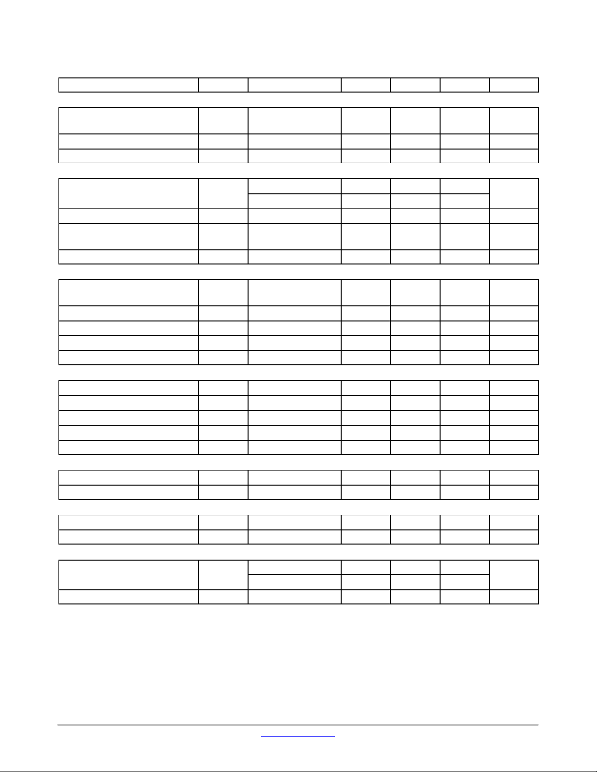
ELECTRICAL CARACTERISTICS At V
Boldface limits apply over the specified temperature range, T
Parameter
= 5 V, TA = +25°C, VCM = 12 V, RL ≥ 10 kW, unless otherwise noted.
S
A = –40°C to 125°C, guaranteed by characterization and/or design.
Symbol Test Conditions Min Typ Max Unit
GAIN
Total Gain, Preamplifier and Buffer
Gain Error G
Gain Drift
DG/DT
G NCS7030
NCS7031
e
TA = −40°C to +125°C +0.3 %
TA = −40°C to +125°C +20
14
20
ppm / °C
INPUT
Input Offset Voltage
V
OS
TA = +25°C ±100 +300
TA = −40°C to +125°C +300
Input Offset Voltage Drift
DV/DT
Common−Mode Rejection Ratio CMRR V
TA = −40°C to +125°C +3
= −5 to 80 V,
CM
90 dB
mV / °C
f = DC to 20 kHz
Input Bias Current (Note 8) I
IB
TBD TBD
PREAMPLIFIER
Gain
Gain Error G
Output Voltage High V
Output Voltage Low V
Output Resistance R
G NCS7030
NCS7031
e
OH
OL
PRE
TA = −40°C to +125°C +0.3 %
V
− 0.1 V
S
98 100 102
7
10
− 0.05 V
S
25 mV
OUTPUT BUFFER
Gain
Gain Error G
Output Voltage High V
Output Voltage Low V
Input Bias Current I
G 2 V/V
+0.3 %
50 mV
OH
OL
IB
e
V
− 0.1 V
S
− 0.05 V
S
40 50 nA
DYNAMIC PERFORMANCE
Signal Bandwidth (−3dB)
BW VID = 0.1 V
p−p
100 kHz
Slew Rate SR VID = 0 to 200 mV step 1
NOISE
Voltage Noise, Peak−to−Peak
Voltage Noise Density e
V
n
N
f = 0.1 Hz to 10 Hz 10
f = 1 kHz 275 nV / ǠHz
POWER SUPPLY
Quiescent Current
I
DD
TA = +25°C 3 TBD
TA = −40°C to +125°C TBD
Power Supply Rejection Ratio PSRR 70 dB
8. Guaranteed by characterization and/or design.
V/V
μV
mA
V/V
kW
V / ms
mV
p−p
mA
www.onsemi.com
4
 Loading...