ON Semiconducto NCP439 User Manual

NCP439
f
2A Very Low Ron Switches
at Low Vin Voltage
The NCP439 is a very low Ron MOSFET controlled by external
logic pin, allowing optimization of battery life, and portable device
autonomy.
This load switch is a best in class in term of R
low V
voltage.
IN
Due to a current consumption optimization with PMOS structure,
leakage currents are eliminated by isolating connected IC’s on the
battery when not used.
Output discharge path is also embedded to eliminate residual
voltages on the output.
Proposed in wide input voltage range from 1.0 V to 3.6 V, and a very
small 0.96 x 0.96 mm WLCSP4, 0.5 mm pitch.
Features
• 1 V – 3.6 V Operating Range
• 37 mW P MOSFET at 1.8 V
• DC Current Up to 2 A
• Output Auto−Discharge
• Active High EN Pin
• WLCSP4 0.96 x 0.96 mm
• This is a Pb−Free Device
optimization at
DS(on)
onsemi.com
www.
MARKING
DIAGRAM
1
WLCSP4
CASE 567FG
AY = Specific Device Code
A = Assembly Location
Y = Year
W = Wafer Lot
PIN DIAGRAM
12
OUT
A
IN
AY
AYW
Typical Applications
• Mobile Phones
• Tablets
• Digital Cameras
• GPS
• Portable Devices
DCDC Converter
or
LDO
ENx
GND
B
(Top View)
EN
ORDERING INFORMATION
See detailed ordering and shipping information on page 8 o
this data sheet.
EN
A2
IN
B2
EN
0
OUT
GND
A1
B1
IC’n
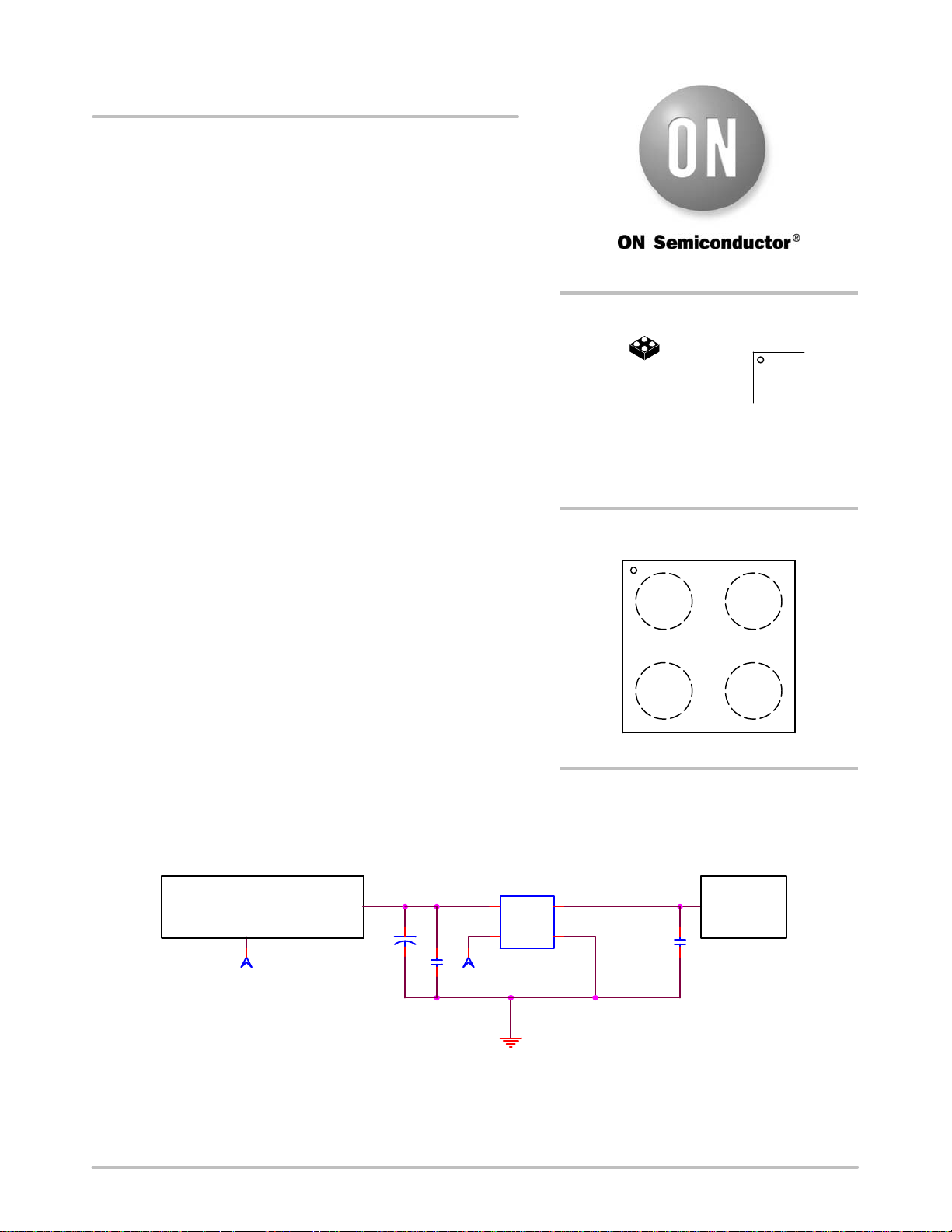
Figure 1. Typical Application Circuit
© Semiconductor Components Industries, LLC, 2013
August, 2016 − Rev. 1
1 Publication Order Number:
NCP439/D

NCP439
PIN FUNCTION DESCRIPTION
Pin Name Pin Number Type Description
IN A2 POWER
GND B1 POWER Ground connection.
EN B2 INPUT Enable input, logic high turns on power switch.
OUT A1 OUTPUT
Load−switch input voltage; connect a 0.1 mF or greater ceramic capacitor from IN to GND as
close as possible to the IC.
Load−switch output; connect a 0.1 mF ceramic capacitor from OUT to GND as close as possible to the IC is recommended.
BLOCK DIAGRAM
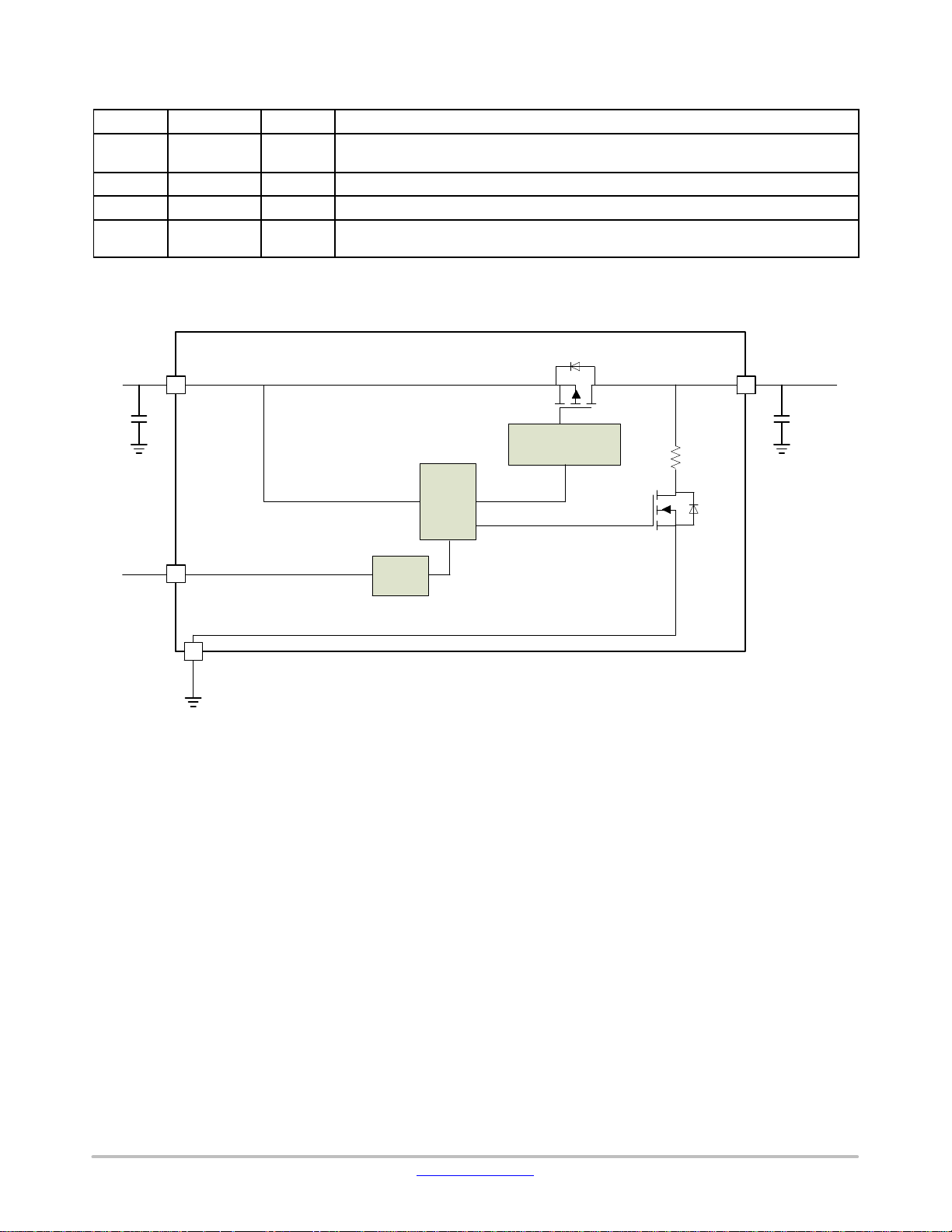
IN: Pin A2
EN: Pin B2
GND: Pin B1
Control
logic
EN block
Figure 2. Block Diagram
Gate driver and soft
start control
OUT: Pin A1
www.onsemi.com
2

NCP439
MAXIMUM RATINGS
Symbol Rating Value Unit
V
EN, VIN,
V
OUT
V
V
IN,
ESD HBM Human Body Model (HBM) ESD Rating are (Notes 1 and 2) 2500 V
ESD MM Machine Model (MM) ESD Rating are (Notes 1 and 2) 250 V
ESD CDM Charge Device Model (CDM) ESD Rating are (Notes 1 and 2) 2000 V
LU Latch−up protection (Note 3)
T
J
T
STG
MSL Moisture Sensitivity (Note 4) Level 1
Stresses exceeding those listed in the Maximum Ratings table may damage the device. If any of these limits are exceeded, device functionality
should not be assumed, damage may occur and reliability may be affected.
1. According to JEDEC standard JESD22−A108.
2. This device series contains ESD protection and passes the following tests:
Human Body Model (HBM) ±2.5 kV per JEDEC standard: JESD22−A114 for all pins.
Machine Model (MM) ±250 V per JEDEC standard: JESD22−A115 for all pins.
Charge Device Model (CDM) ±2.0 kV per JEDEC standard: JESD22−C101 for all pins.
3. Latch up Current Maximum Rating: ±100 mA per JEDEC standard: JESD78 class II.
4. Moisture Sensitivity Level (MSL): 1 per IPC/JEDEC standard: J−STD−020.
IN, OUT, EN, Pins −0.3 to + 4.0 V
From IN to OUT Pins: Input/Output 0 to + 4.0 V
OUT
100 mA
− Pins IN, OUT, EN
Maximum Junction Temperature −40 to + 125 °C
Storage Temperature Range −40 to + 150 °C
OPERATING CONDITIONS
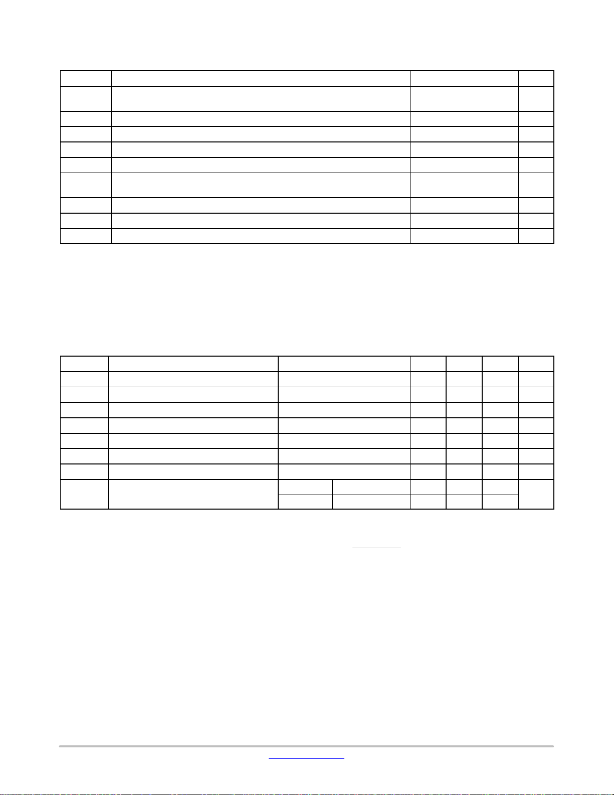
Symbol Parameter Conditions Min Typ Max Unit
V
IN
V
EN
T
A
C
IN
C
OUT
R
q
JA
I
OUT
P
D
5. The R
6. The maximum power dissipation (P
Operational Power Supply 1.0 3.6 V
Enable Voltage 0 3.6
Ambient Temperature Range −40 25 + 85 °C
Decoupling input capacitor 0.1
Decoupling output capacitor 0.1
Thermal Resistance Junction to Air WLCSP package (Note 5) 100 °C/W
Maximum DC current 2 A
Power Dissipation Rating (Note 6)
TA ≤ 25°C WLCSP package 0.5
TA = 85°C WLCSP package 0.2
is dependent of the PCB heat dissipation and thermal via.
q
JA
) is given by the following formula:
D
T
* T
P
JMAX
+
D
A
R
qJA
mF
mF
W
www.onsemi.com
3
 Loading...