LDO Regulator - Very Low
Dropout, CMOS, Bias Rail
700 mA
NCP137
The NCP137 is a 700 mA VLDO equipped with NMOS pass
transistor and a separate bias supply voltage (V
provides very stable, accurate output voltage with low noise suitable
for space constrained, noise sensitive applications. In order to
optimize performance for battery operated portable applications, the
NCP137 features low I
consumption. The WLCSP6 1.2 mm x
Q
0.8 mm Chip Scale package is optimized for use in space constrained
applications.
Features
• Input Voltage Range: V
OUT
to 5.5 V
• Bias Voltage Range: 2.5 V to 5.5 V
• Adjustable and Fixed Voltage Version Available
• Output Voltage Range: 0.4 V to 1.8 V (Fixed) and
Output Voltage Range: 0.5 V to 3.0 V (Adjustable)
• ±1% Accuracy over Temperature, 0.5% V
OUT
• Ultra−Low Dropout: Typ. 40 mV at 700 mA
• Very Low Bias Input Current of Typ. 35 mA
• Very Low Bias Input Current in Disable Mode: Typ. 0.5 mA
• Logic Level Enable Input for ON/OFF Control
• Output Active Discharge Option Available
• Stable with a 4.7 mF Ceramic Capacitor
• Available in WLCSP6 − 1.2 mm x 0.8 mm, 0.4 mm pitch Package
• These Devices are Pb−Free, Halogen Free/BFR Free and are RoHS
Compliant
). The device
BIAS
@ 25°C
www.onsemi.com
WLCSP6, 1.2x0.8
CASE 567MV
XX = Specific Device Code
M = Month Code
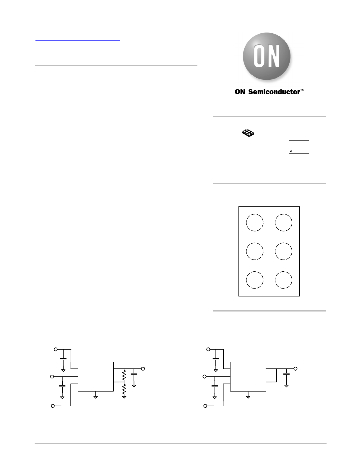
PIN CONNECTIONS
12
A
VOUT VIN
B
SNS/FB
C
GND
MARKING
DIAGRAM
XXM
EN
VBIAS
Typical Applications
• Battery−powered Equipment
• Smartphones, Tablets
• Cameras, DVRs, STB and Camcorders
V
BIAS
≥2.5 V
1 mF
V
IN
1.02 V
4.7 mF
V
EN
© Semiconductor Components Industries, LLC, 2016
January, 2021 − Rev. 6
NCP137 − ADJ
BIAS
IN
EN
GND
OUT
R1
FB
R2
See detailed ordering, marking and shipping information on
page 7 of this data sheet.
V
BIAS
V
OUT
0.9 V up to 700 mA
4.7 mF
≥2.5 V
V
1.02 V
V
1 mF
IN
4.7 mF
EN
Figure 1. Typical Application Schematics
1 Publication Order Number:
Top View
ORDERING INFORMATION
V
0.9 V up to 700 mA
10 mF
BIAS
IN
EN
NCP137
OUT
SNS
GND
OUT
NCP137/D

NCP137
IN
EN
BIAS
GND
IN
CURRENT
LIMIT
ENABLE
BLOCK
UVLO
0.50 V
VOLTAGE
REFERENCE
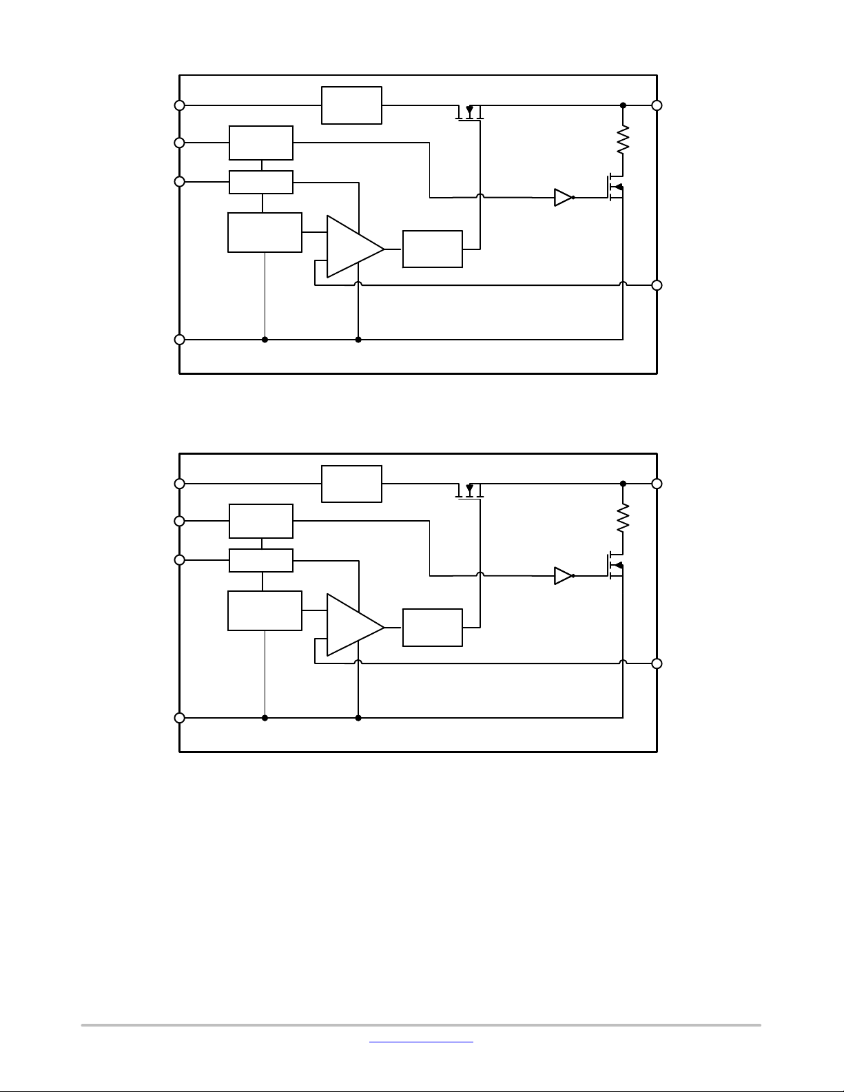
*Active output discharge function is present only in NCP137A option devices.
+
−
THERMAL
LIMIT
DISCHARGE
150 W
*Active
Figure 2. Simplified Schematic Block Diagram − Adjustable Version
CURRENT
LIMIT
OUT
FB
OUT
EN
BIAS
GND
ENABLE
BLOCK
UVLO
VOLTAGE
REFERENCE
*Active output discharge function is present only in NCP137A option devices.
+
−
THERMAL
LIMIT
DISCHARGE
150 W
*Active
Figure 3. Simplified Schematic Block Diagram − Fixed Version
SNS
www.onsemi.com
2

NCP137
PIN FUNCTION DESCRIPTION
Pin No.
WLCSP6
A1 VOUT Regulated Output Voltage pin
A2 VIN Input Voltage Supply pin
B1
(ADJ devices)
B1
(Fix Volt devices)
B2 EN Enable pin. Driving this pin high enables the regulator. Driving this pin low puts the regulator into
C1 GND Ground pin
C2 VBIAS Bias voltage supply for internal control circuits. This pin is monitored by internal Under-Voltage
ABSOLUTE MAXIMUM RATINGS
Input Voltage (Note 1) V
Output Voltage V
Chip Enable, Bias, FB and SNS Input V
Output Short Circuit Duration t
Maximum Junction Temperature T
Storage Temperature T
ESD Capability, Human Body Model (Note 2) ESD
ESD Capability, Machine Model (Note 2) ESD
Stresses exceeding those listed in the Maximum Ratings table may damage the device. If any of these limits are exceeded, device functionality
should not be assumed, damage may occur and reliability may be affected.
1. Refer to ELECTRICAL CHARACTERISTICS and APPLICATION INFORMATION for Safe Operating Area.
2. This device series incorporates ESD protection (except OUT pin) and is tested by the following methods:
ESD Human Body Model tested per EIA/JESD22−A114
ESD Machine Model tested per EIA/JESD22−A115
Latchup Current Maximum Rating tested per JEDEC standard: JESD78.
Pin Name Description
FB Adjustable Regulator Feedback Input. Connect to output voltage resistor divider central node.
SNS Output voltage Sensing Input. Connect to Output on the PCB to output the voltage
corresponding to the part version.
shutdown mode.
Lockout Circuit.
Rating Symbol Value Unit
IN
OUT
EN, VBIAS, VFB, VSNS
SC
J
STG
HBM
MM
−0.3 to 6 V
−0.3 to (VIN+0.3) ≤ 6 V
−0.3 to 6 V
unlimited s
150 °C
−55 to 150 °C
2000 V
200 V
THERMAL CHARACTERISTICS
Rating Symbol Value Unit
Thermal Characteristics, WLCSP6 1.2 mm x 0.8 mm
Thermal Resistance, Junction−to−Air (Note 3)
R
q
JA
69 °C/W
3. This junction−to−ambient thermal resistance under natural convection was derived by thermal simulations based on the JEDEC JESD51
series standards methodology. Only a single device mounted at the center of a high_K (2s2p) 80 mm x 80 mm multilayer board with 1−ounce
internal planes and 2−ounce copper on top and bottom. Top copper layer has a dedicated 1.6 sqmm copper area.
www.onsemi.com
3
 Loading...