Power Factor Corrected
LED Driver with Primary
Side CC/CV
NCL30488
The NCL30488 is a power factor corrected flyback controller
targeting isolated constant current LED drivers. The controller
operates in a quasi−resonant mode to provide high efficiency. Thanks
to a novel control method, the device is able to tightly regulate a
constant LED current from the primary side. This removes the need
for secondary side feedback circuitry, its biasing and for an
optocoupler.
The device is highly integrated with a minimum number of external
components. A robust suite of safety protection is built in to simplify
the design.
Features
• High Voltage Startup
• Quasi−resonant Peak Current−mode Control Operation
• Primary Side Feedback
• CC / CV Accurate Control V
• Tight LED Constant Current Regulation of ±2% Typical
• Digital Power Factor Correction
• Analog and Digital Dimming
• Cycle by Cycle Peak Current Limit
• Wide Operating V
CC
Range
• −40 to + 125°C
• Robust Protection Features
♦ Brown−Out
♦ OVP on V
Constant Voltage / LED Open Circuit Protection
♦
♦ Winding Short Circuit Protection
♦ Secondary Diode Short Protection
♦ Output Short Circuit Protection
♦ Thermal Shutdown
♦ Line over Voltage Protection
CC
• This is a Pb−Free Device
Typical Applications
• Integral LED Bulbs
• LED Power Driver Supplies
• LED Light Engines
up to 320 V rms
in
www.onsemi.com
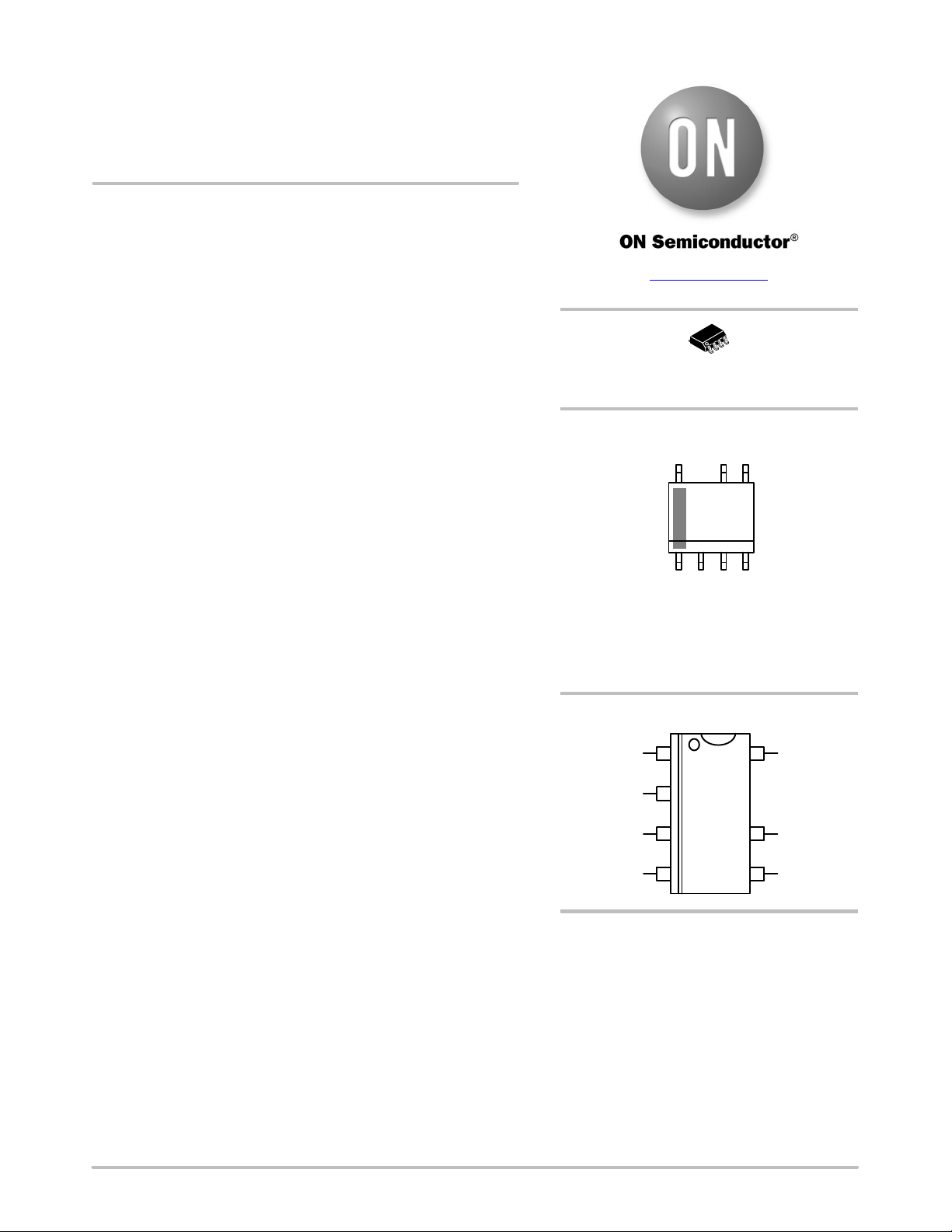
SOIC−7
CASE 751U
MARKING
DIAGRAM
8
L30488XX
ALYWX
G
1
L30488 = Specific Device Code
XX = Version
A = Assembly Location
L = Wafer Lot
YW = Assembly Start Week
G = Pb−Free Package
PIN CONNECTIONS
COMP
GND
See detailed ordering and shipping information on page 21 of
this data sheet.
1
ZCD
2
3
CS
4
ORDERING INFORMATION
HV
8
VCC
6
DRV
5
© Semiconductor Components Industries, LLC, 2020
April, 2021 − Rev. 1
1 Publication Order Number:
NCL30488/D
NCL30488
NCL30488
1
2
3
45
7
6
.
.
.
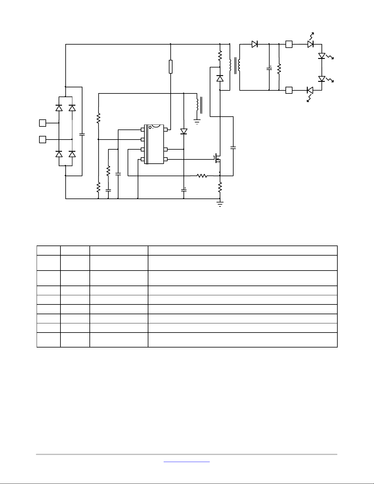
Figure 1. Typical Application Schematic for NCL30488
PIN FUNCTION DESCRIPTION NCL30488
Pin N5 Pin Name Function Pin Description
1 COMP OTA output for CV loop This pin receives a compensation network (capacitors and resistors) to stabilize the
2 ZCD Zero crossing Detection
V
sensing
aux
3 CS Current sense This pin monitors the primary peak current.
4 GND − The controller ground
5 DRV Driver output The driver’s output to an external MOSFET
6 VCC Supplies the controller This pin is connected to an external auxiliary voltage.
7 NC creepage
8 HV High Voltage sensing This pin connects after the diode bridge to provide the startup current and internal
CV loop
This pin connects to the auxiliary winding and is used to detect the core reset event.
This pin also senses the auxiliary winding voltage for accurate output voltage control.
high voltage sensing function.
www.onsemi.com
2
COMP
ZCD
Constant Voltage
Control
Zero crossing detection Logic
(ZCD blanking,Time−Out, …)
Aux . Winding Short Circuit Prot.
Standby
V
CV
Slow_OVP
Fast_OVP
NCL30488
INTERNAL CIRCUIT ARCHITECTURE
STOP
L_OVP
Aux_SCP
Fast_OVP
Thermal
Shutdown
Aux_SCP
Fault
Management
CS_short
V
REFXVVS
Valley Selection
Frequency foldback
Slow_OVP
UVLO
VCC_OVP
OFF
VCC Management
BO_NOK
L_OVP
V
HVdiv
VCC
OVP
Brown−out
Line OVP
HV
Startup
VCC
HV
CS
GND
Line
feed −forward
Leading
Edge
Blanking
Q_drv
V
HVdiv
STOP
V
Standby
HVdiv
V
Ipk_max
WOD_SCP
CS_short
REFX
CS_reset
STOP
Power factor and
Constant−current control
Max. P eak
Current Limit
Winding /
Output diode
SCP
CS Short
Protection
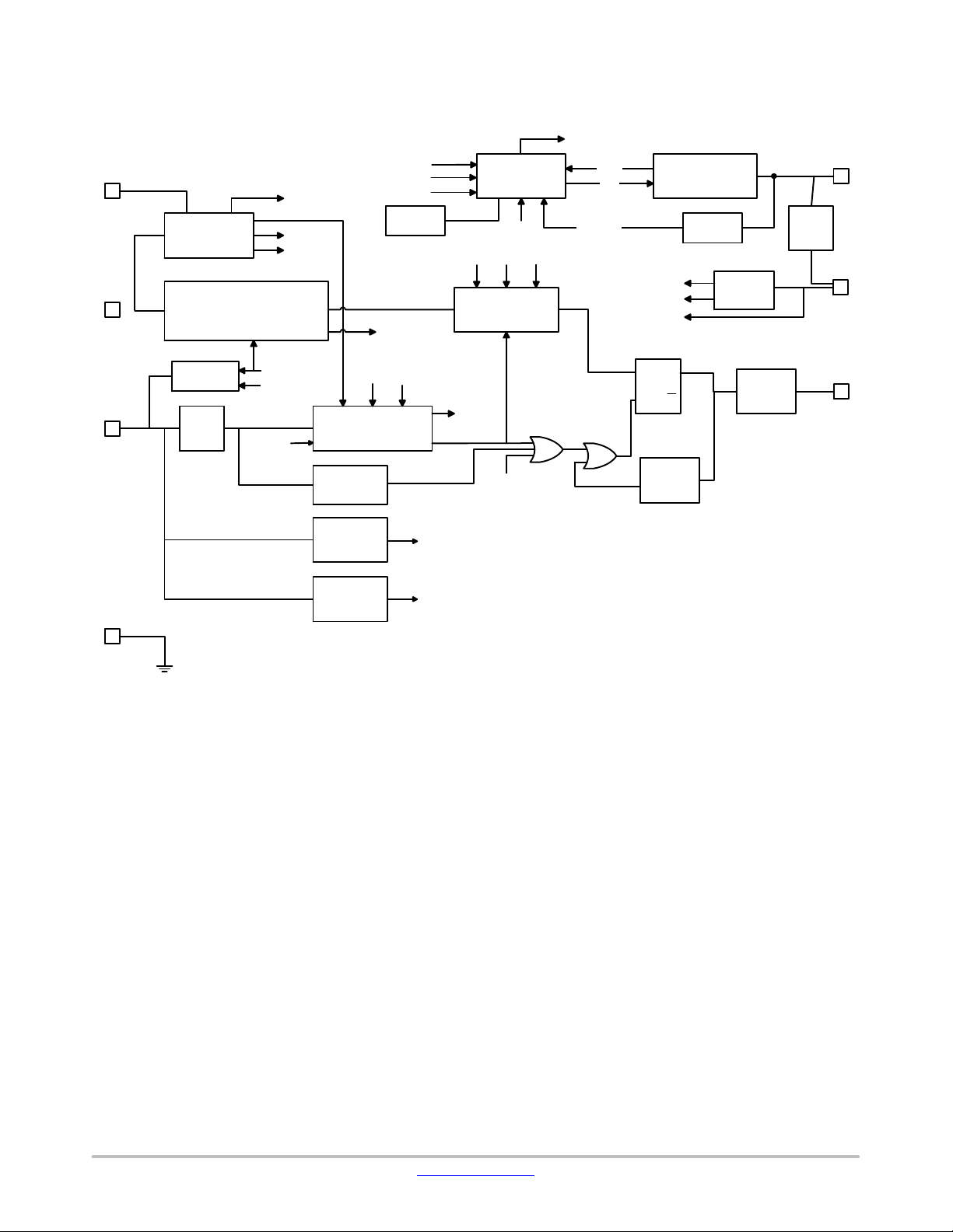
Figure 2. Internal Circuit Architecture NCL30488
S
RQQ
Maximum
on−time
Q_drv
Driver
and
Clamp
DRV
www.onsemi.com
3
NCL30488
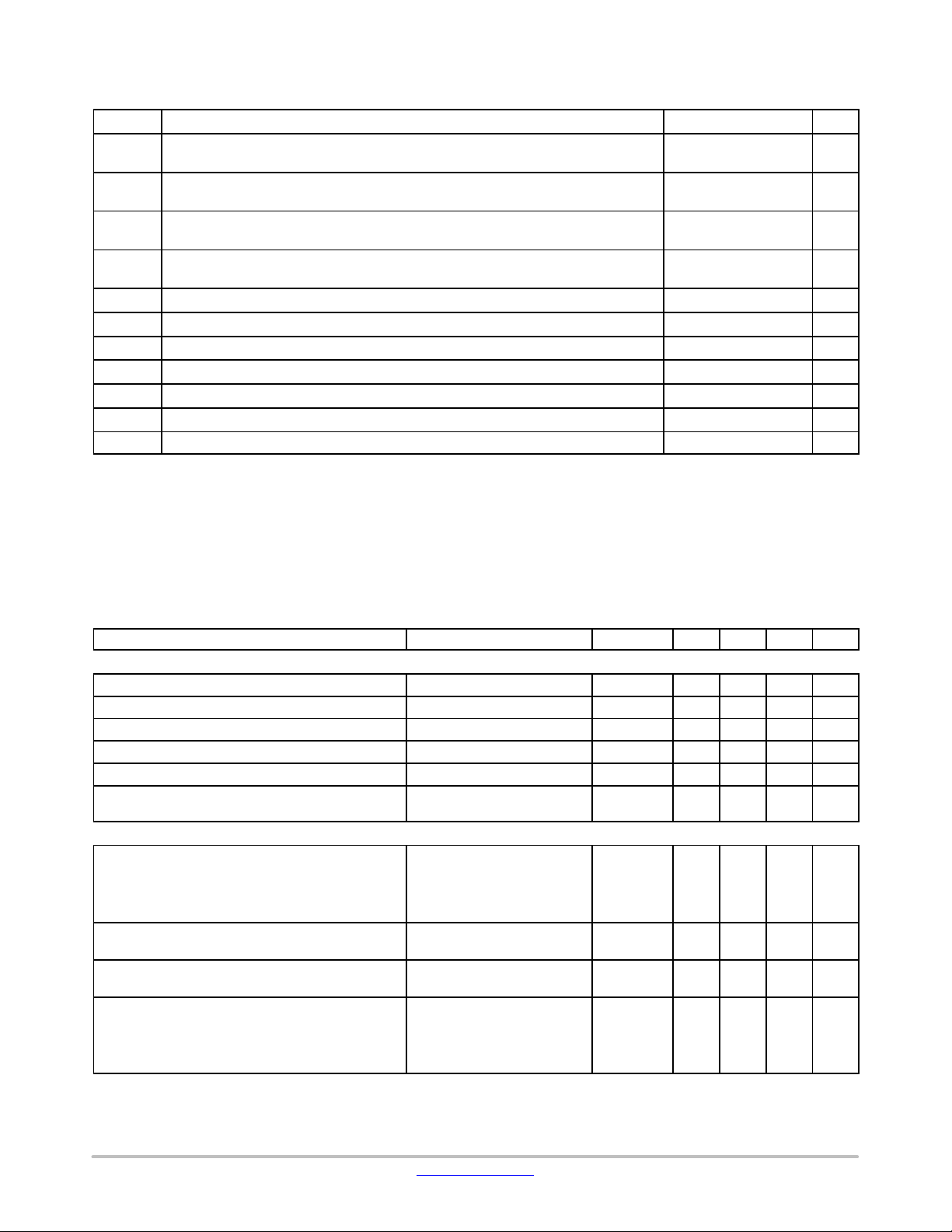
MAXIMUM RATINGS TABLE
Symbol Rating Value Unit
V
CC(MAX)
I
CC(MAX)
V
DRV(MAX)
I
DRV(MAX)
V
HV(MAX)
I
HV(MAX)
V
MAX
I
MAX
R
θ
T
J(MAX)
Stresses exceeding those listed in the Maximum Ratings table may damage the device. If any of these limits are exceeded, device functionality
should not be assumed, damage may occur and reliability may be affected.
1. V
DRV
2. This level is low enough to guarantee not to exceed the internal ESD diode and 5.5 V ZENER diode. More positive and negative voltages
can be applied if the pin current stays within the −2 mA / 5 mA range.
3. This device series contains ESD protection and exceeds the following tests: Human Body Model 4000 V per Mil−Std−883, Method 3015.
Charged Device Model 1000 V per JEDEC Standard JESD22−C101D.
4. This device contains latch−up protection and exceeds 100 mA per JEDEC Standard JESD78.
Maximum Power Supply voltage, VCC pin, continuous voltage
Maximum current for VCC pin
Maximum driver pin voltage, DRV pin, continuous voltage
Maximum current for DRV pin
Maximum voltage on HV pin
Maximum current for HV pin (dc current self−limited if operated within the allowed range)
Maximum voltage on low power pins (except pins DRV and VCC)
Current range for low power pins (except pins DRV and VCC)
Thermal Resistance Junction−to−Air 200 °C/W
J−A
−0.3 to 30
Internally limited
−0.3, V
(Note 1)
DRV
−300, +500
−0.3, +700
±20
−0.3, 5.5 (Note 2)
−2, +5
Maximum Junction Temperature 150 °C
Operating Temperature Range −40 to +125 °C
Storage Temperature Range −60 to +150 °C
ESD Capability, HBM model except HV pin (Note 3) 4 kV
ESD Capability, HBM model HV pin 1.5 kV
ESD Capability, CDM model (Note 3) 1 kV
is the DRV clamp voltage V
when VCC is higher than V
DRV(high)
DRV(high)
. V
is VCC otherwise.
DRV
V
mA
V
mA
V
mA
V
mA
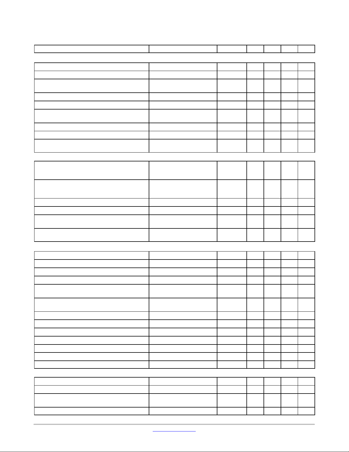
ELECTRICAL CHARACTERISTICS (Unless otherwise noted: For typical values T
For min/max values T
= −40°C to +125°C, Max TJ = 150°C, VCC = 12 V)
J
Parameter
Test Condition Symbol Min Typ Max Unit
J
HIGH VOLTAGE SECTION
High voltage current source VCC = V
– 200 mV I
CC(on)
High voltage current source VCC = 0 V I
VCC level for I
HV(start1)
to I
transition V
HV(start2)
Minimum startup voltage VCC = 0 V V
HV source leakage current VHV = 450 V I
Maximum input voltage (rms) for correct operation of
the PFC loop
SUPPLY SECTION
Supply Voltage
Startup Threshold
Minimum Operating Voltage
Hysteresis V
Internal logic reset
CC(on)
– V
CC(off)
VCC increasing
VCC decreasing
VCC decreasing
Over Voltage Protection
VCC OVP threshold
V
noise filter (Note 5)
CC(off)
V
noise filter (Note 5)
CC(reset)
Supply Current
Device Disabled/Fault
Device Enabled/No output load on pin 5
Device Switching (F
Device switching (F
= 65 kHz)
sw
= 700 Hz)
sw
VCC > V
CC(off)
Fsw = 65 kHz
C
= 470 pF, Fsw = 65 kHz
DRV
V
v 0.9 V
COMP
= 25°C, VCC = 12 V, V
HV(start2)
HV(start1)
CC(TH)
HV(MIN)
HV(leak)
V
HV(OL)
V
CC(on)
V
CC(off)
V
CC(HYS)
V
CC(reset)
V
CC(OVP)
t
VCC(off)
t
VCC(reset)
I
CC1
I
CC2
I
CC3
I
CC4
3.9 5.1 6.2 mA
− 300 −
− 0.8 − V
− 15 − V
− 4.5 10
320 − − V rms
16
9.3
7.6
4
25 26.5 28 V
−
−
1.2
–
−
−
= 0 V, VCS = 0 V)
ZCD
18
10.2
−
5
5
20
1.35
3.0
3.5
1.7
20
10.7
−
6
−
−
1.6
3.5
4.0
1.88
mA
mA
V
ms
mA
www.onsemi.com
4
NCL30488
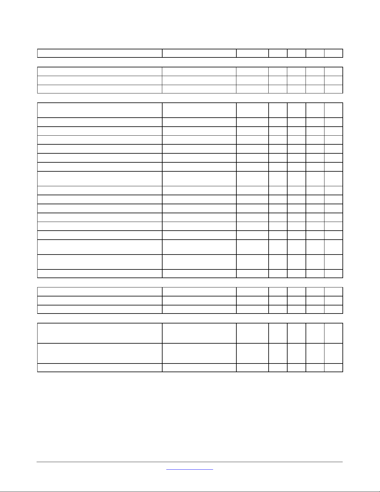
ELECTRICAL CHARACTERISTICS (Unless otherwise noted: For typical values T
For min/max values T
= −40°C to +125°C, Max TJ = 150°C, VCC = 12 V) (continued)
J
= 25°C, VCC = 12 V, V
J
Parameter UnitMaxTypMinSymbolTest Condition
CURRENT SENSE
Maximum Internal current limit
Leading Edge Blanking Duration for V
ILIM
Propagation delay from current detection to gate
off−state
Maximum on−time (option 1) t
Maximum on−time (option 2) t
Threshold for immediate fault protection activation
(140% of V
Leading Edge Blanking Duration for V
ILIM
)
CS(stop)
Current source for CS to GND short detection I
Current sense threshold for CS to GND short
VCS rising V
detection
GATE DRIVE
Drive Resistance
DRV Sink
DRV Source
Drive current capability
DRV Sink (Note GBD)
DRV Source (Note GBD)
Rise Time (10% to 90%) C
Fall Time (90 %to 10%) C
DRV Low Voltage VCC = V
DRV High Voltage VCC = V
= 470 pF t
DRV
= 470 pF t
DRV
+0.2 V
CC(off)
C
C
DRV
DRV
= 470 pF, R
CC(MAX)
= 470 pF, R
DRV
DRV
= 33 kW
= 33 kW
ZERO VOLTAGE DETECTION CIRCUIT
Upper ZCD threshold voltage
Lower ZCD threshold voltage V
Threshold to force V
maximum during startup V
REFX
V
rising V
ZCD
falling V
ZCD
falling V
ZCD
ZCD hysteresis V
Propagation Delay from valley detection to DRV high
(no t
LEB4
)
Additional delay from valley lockout output to DRV
latch set (programmable option)
V
decreasing t
ZCD
V
decreasing T
ZCD
Equivalent time constant for ZCD input (GBD) t
Blanking delay after on−time (option 1) V
Blanking delay after on−time (option 2) V
Blanking Delay at light load (option 1) V
Blanking Delay at light load (option 2) V
> 0.35 V t
REFX
> 0.35 V t
REFX
< 0.25 V t
REFX
< 0.25 V t
REFX
Timeout after last DEMAG transition t
Pulling−down resistor V
ZCD
= V
ZCD(falling)
CONSTANT CURRENT CONTROL
Reference Voltage Tj = 25°C − 85°C V
Reference Voltage Tj = −40°C to 125°C V
Current sense lower threshold for detection of the
VCS falling V
leakage inductance reset time
Blanking time for leakage inductance reset detection t
V
ILIM
t
LEB
t
ILIM
on(MAX)
on(MAX)
V
CS(stop)
t
BCS
CS(short)
CS(low)
R
SNK
R
SRC
I
SNK
I
SRC
r
f
V
DRV(low)
V
DRV(high)
ZCD(rising)
ZCD(falling)
ZCD(start)
ZCD(HYS)
ZCD(DEM)
LEB4
PAR
ZCD(blank1)
ZCD(blank1)
ZCD(blank2)
ZCD(blank2)
TIMO
R
ZCD(pd)
REF/3
REF/3
CS(low)
CS(low)
= 0 V, VCS = 0 V)
ZCD
1.33 1.40 1.47 V
283 345 407 ns
− 100 150 ns
29 39 49
16 20 24
ms
ms
1.9 2.0 2.1 V
− 170 − ns
400 500 600
mA
20 60 90 mV
W
−
13
−
30
−
−
mA
−
500
−
300
−
−
– 30 − ns
– 20 − ns
8 – − V
10 12 14 V
− 90 150 mV
35 55 − mV
− 0.7 − V
15 − − mV
− − 150 ns
125 250 375 ns
− 20 − ns
1.1 1.5 1.9
0.75 1.0 1.25
0.6 0.8 1.0
0.45 0.6 0.75
5 6.5 8
− 200 −
ms
ms
ms
ms
ms
kW
327.9 334.2 341.2 mV
324 334.2 346 mV
20 50 100 mV
− 120 − ns
www.onsemi.com
5
NCL30488
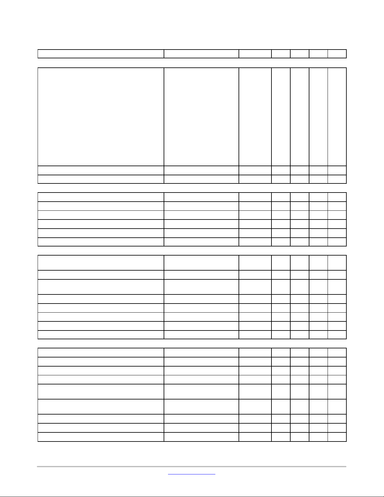
ELECTRICAL CHARACTERISTICS (Unless otherwise noted: For typical values T
For min/max values T
= −40°C to +125°C, Max TJ = 150°C, VCC = 12 V) (continued)
J
= 25°C, VCC = 12 V, V
J
Parameter UnitMaxTypMinSymbolTest Condition
POWER FACTOR CORRECTION
Clamping value for V
REF(PFC)
TJ = 0°C to 125°C V
REF(PFC)CLP
Line range detector for PFC loop VHV increases V
Line range detector for PFC loop VHV decreases V
CONSTANT VOLTAGE SECTION
Internal voltage reference for constant voltage
regulation
CV Error amplifier Gain G
Error amplifier current capability V
REFX
= V
(no dimming) I
REF
COMP pin lower clamp voltage V
COMP pin higher clamp voltage TJ = 0°C to 125°C V
COMP pin higher clamp voltage TJ = −40°C to 125°C V
Internal divider V
Internal ZCD voltage below which the CV OTA is
boosted
Threshold for releasing the CV boost V
COMP
to V
REFX
V
REF(CV)
REF(CV)
* 85% V
* 90% V
boost(CV)RST
Error amplifier current capability during boost phase I
ZCD OVP 1st level (slow OVP) option 1 V
ZCD voltage at which slow OVP is exit (option 1) V
* 115% V
REF(CV)
* 105% V
REF(CV)
Switching period during slow OVP T
ZCD fast OVP option 1 V
Number of switching cycles before fast OVP
* 125% + 150 mV V
ref(CV)
T
confirmation
Duration for disabling DRV pulses during ZCD fast
OVP
COMP pin internal pullup resistor (SSR option) R
LINE FEED FORWARD
VHV to I
conversion ratio K
CS(offset)
Offset current maximum value VHV > (450 V or 500 V) I
Line feed−forward current DRV high, V
= 200 V I
HV
VALLEY LOCKOUT SECTION
REFX
REFX
increasing
HV
> 80% V
> 80% V
REF
REF
Threshold for line range detection V
st
(1
to 2nd valley transition for V
(prog. option: 1st to 3rd valley transition)
Threshold for line range detection VHV decreasing
nd
(2
to 1st valley transition for V
(prog. option: 3rd to 1st valley transition)
VHV increases V
)
VHV decreases V
)
Blanking time for line range detection t
HL(PFC)
LL(PFC)
V
REF(CV)
EA
EA
CV(clampL)
CV(clampH)
CV(clampH)
K
COMP
boost(CV)
EAboost
OVP1
OVP1rst
sw(OVP1)
OVP2
OVP2_CNT
T
recovery
pullup
LFF
offset(MAX)
FF
HL
LL
HL(blank)
= 0 V, VCS = 0 V)
ZCD
2.06 2.2 2.34 V
− 240 − Vdc
− 230 − Vdc
3.41 3.52 3.63 V
40 50 60
− ±60 −
− 0.6 − V
4.05 4.12 4.25 V
4.01 4.12 4.25 V
− 4 −
2.796 2.975 3.154 V
2.96 3.15 3.34 V
− ±140 −
3.783 4.025 4.267 V
− 3.675 − V
− 1.5 − ms
4.253 4.525 4.797 V
− 4 −
− 4 − s
− 15 −
0.189 0.21 0.231
mA/V
76 95 114
35 40 45
228 240 252 V
218 230 242 V
15 25 35 ms
mS
mA
mA
kW
mA
mA
www.onsemi.com
6
NCL30488
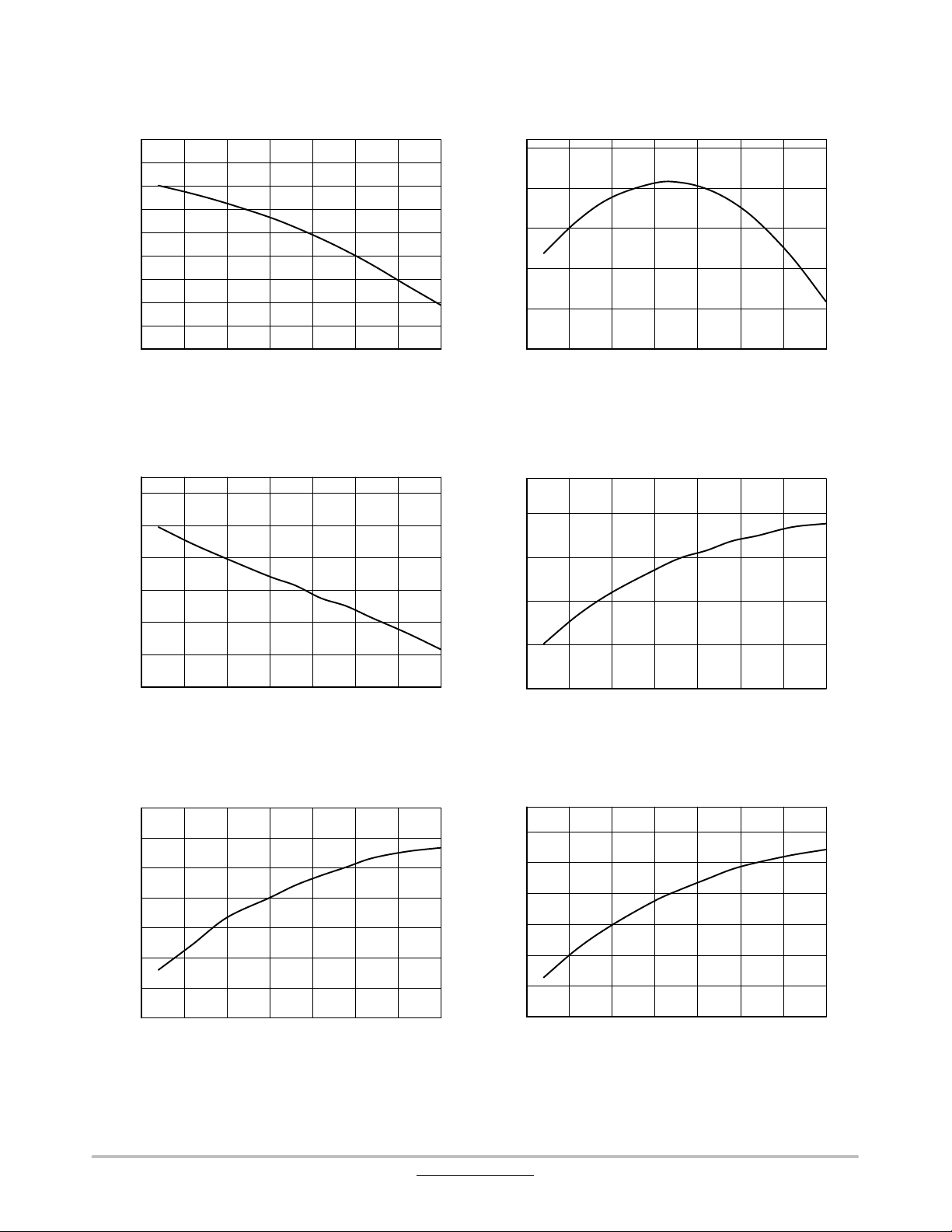
ELECTRICAL CHARACTERISTICS (Unless otherwise noted: For typical values T
For min/max values T
= −40°C to +125°C, Max TJ = 150°C, VCC = 12 V) (continued)
J
= 25°C, VCC = 12 V, V
J
= 0 V, VCS = 0 V)
ZCD
Parameter UnitMaxTypMinSymbolTest Condition
VALLEY LOCKOUT SECTION
Valley thresholds
st
to 2nd valley transition at LL and 2nd to 3rd valley
1
HL, V
2
HL, V
2
HL, V
3rd to 2nd valley transition at LL and 4th to 3rd valley
HL, V
3
HL, V
4th to 3th valley transition at LL and 5th to 4th valley
HL, V
4th to 5th valley transition at LL and 5th to 6th valley
HL, V
5th to 4th valley transition at LL and 6th to 5th valley
HL, V
V
V
decr. (prog. option: 3rd to 4th valley HL)
REF
nd
to 1st valley transition at LL and 3rd to 2nd valley
incr. (prog. option: 4th to 3rd valley HL)
REF
nd
to 3rd valley transition at LL and 3rd to 4th valley
decr. (prog. option: 4th to 5th valley HL)
REF
incr. (prog. option: 5th to 4th valley HL)
REF
rd
to 4th valley transition at LL and 4th to 5th valley
decr. (prog. option: 5th to 6th valley HL)
REF
incr. (prog. option: 6th to 5th valley HL)
REF
decr. (prog. option: 6th to 7th valley HL)
REF
incr. (prog. option: 7th to 6th valley HL)
REF
value at which the FF mode is activated V
REF
value at which the FF mode is removed V
REF
V
decreases
REF
increases
V
REF
V
decreases
REF
V
increases
REF
V
decreases
REF
V
increases
REF
V
decreases
REF
V
increases
REF
decreases V
REF
increases V
REF
V
VLY1−2/2−3
V
VLY2−1/3−2
V
VLY2−3/3−4
V
VLY3−2/4−3
V
VLY3−4/4−5
V
VLY4−3/5−4
V
VLY4−5/5−6
V
VLY5−4/6−5
FFstart
FFstop
−
0.80
−
0.90
−
0.65
−
0.75
−
0.50
−
0.60
−
0.35
−
0.45
− 0.25 − V
− 0.35 − V
V
−
−
−
−
−
−
−
−
FREQUENCY FOLDBACK
Added dead time
Added dead time V
Dead−time clamp ( option 1) V
Dead−time clamp ( option 2) V
Minimum added dead−time in standby V
Maximum added dead−time in standby (option 2) V
V
= 0.25 V t
REFX
= 0.08 V t
REFX
< 3 mV t
REFX
< 11.2 mV t
REFX
= 0 t
REFX
REFX
= 0, V
< 0.7 V t
COMP
FF1LL
FFchg
FFend1
FFend2
DT(min)SBY
DT(max)SBY2
0.8 1.0 1.2
− 40 −
− 675 −
− 250 −
− 650 −
− 1.8 − ms
ms
ms
ms
ms
ms
FAULT PROTECTION
Thermal Shutdown (Note 5) Device switching (F
around 65 kHz)
SW
Thermal Shutdown Hysteresis T
Threshold voltage for output short circuit or aux.
winding short circuit detection
Short circuit detection Timer V
ZCD
< V
ZCD(short)
Auto−recovery Timer t
Line OVP threshold VHV increasing V
HV pin voltage at which Line OVP is reset VHV decreasing V
Blanking time for line OVP reset T
T
SHDN
SHDN(HYS)
V
ZCD(short)
t
OVLD
recovery
HV(OVP)
HV(OVP)RST
LOVP(blank)
130 150 170 °C
− 20 – °C
0.6 0.65 0.7 V
70 90 110 ms
3 4 5 s
457 469 485 Vdc
430 443 465 Vdc
15 25 35 ms
BROWN−OUT AND LINE SENSING
Brown−Out ON level (IC start pulsing) VHV increasing V
Brown−Out ON level (IC start pulsing) option 2 VHV increasing V
Brown−Out OFF level (IC stops pulsing) VHV decreasing V
Brown−Out OFF level (IC stops pulsing) option 2 VHV decreasing V
HV pin voltage above which the sampling of ZCD is
enabled low line
HV pin voltage above which the sampling of ZCD is
enabled highline
V
decreasing, low line V
HV
V
decreasing, highline V
HV
ZCD sampling enable comparator hysteresis VHV increasing V
BO comparators delay t
Brown−Out blanking time t
HVBO(on)
HVBO(on)2
HVBO(off)
HVBO(off)2
sampENLL
sampENHL
sampHYS
BO(delay)
BO(blank)
101.5 108 114.5 Vdc
129.7 138 146.3 Vdc
92 98 104 Vdc
121 129 137 Vdc
− 55 − V
− 105 − V
− 5 − V
− 30 −
ms
15 25 35 ms
Product parametric performance is indicated in the Electrical Characteristics for the listed test conditions, unless otherwise noted. Product
performance may not be indicated by the Electrical Characteristics if operated under different conditions.
5. Guaranteed by design.
www.onsemi.com
7
NCL30488
TYPICAL CHARACTERISTICS
5,4
5,3
5,2
5,1
5
(mA)
4,9
HV(start2)
4,8
I
4,7
4,6
4,5
−50 −25 0 25 50 75 100 125
TEMPERATURE (°C)
361
359
357
(V rms)
355
HV(OL)
353
V
351
Figure 3. I
HV(start2)
vs. Temperature Figure 4. I
309
304
299
(mA)
294
HV(start1)
I
289
284
−50 −25 0 25 50 75 100 125
TEMPERATURE (°C)
vs. Temperature
18,34
18,29
(V)
18,24
CC(on)
V
18,19
HV(start1)
349
−50 −25 0 25 50 75 100 125
TEMPERATURE (°C) TEMPERATURE (°C)
Figure 5. V
10,25
10,23
10,21
10,19
(V)
10,17
CC(off)
V
10,15
10,13
10,11
−50 −25 0 25 50 75 100 125
vs. Temperature Figure 6. V
HV(OL)
TEMPERATURE (°C) TEMPERATURE (°C)
Figure 7. V
vs. Temperature Figure 8. V
CC(off)
18,14
−50 −25 0 25 50 75 100 125
vs. Temperature
CC(on)
26,96
26,91
26,86
(V)
26,81
CC(OVP)
V
26,76
26,71
26,66
−50 −25 0 25 50 75 100 125
vs. Temperature
CC(OVP)
www.onsemi.com
8
 Loading...