Onkyo TXDS-575 Schematic

Part 1
Analog Processing
TX-DS575 / TX-DS575X
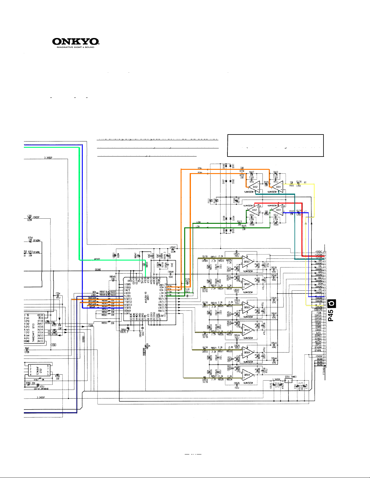
Pin 31 and 32 balanced input for Right channel(RED); Pin 29 and 30 balanced input for Left channel (GREEN
)
pg () p ()
g
ggg
The analog signal that goes in at Pin 29 32 does not
Q101 services as inverting amplifier
come come out as analog through Pin 23 28 before it
ocessed as above
While Q102 non inverting. Note correction
as a c a ce o be g p ocessed as abo e
6
6
5
5
Q8501 have combination of ADC and DAC.
Pin 29 ~32 are balanced inputs to ADC. Internaly the analog signal
oes through High Pass Limiter before it is clocked to L/R out.
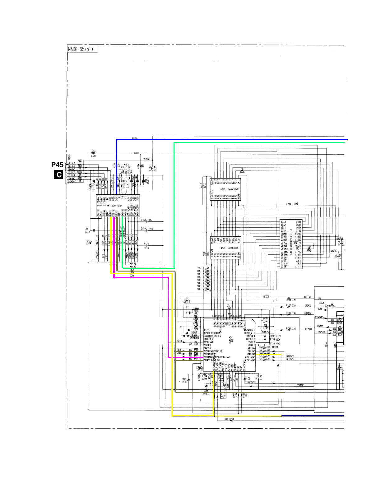
Master Clock MCK02 is made available from at Pin 39. Source of MCK02 is Q114.
Pin 9 provides a serial audio data output derived from the analog inputs 29~32 whose data rate is dependant on
L/R Clock at Pin 5 and Master Clock at Pin 39. The L/R clock and Serial Data may look alike
except Pin 9 has data incorpoarted within the L/R clock. Pin 9 serial data will arrive at Q114 at Pin 8.
"
has a chance of being pr
~
~
"
On PIN 5,6,.

Analog Processing
TX-DS575 / TX-DS575X
Part 2
A
udio Data from Q8501 Pin 9 arrives at Pin 8 of Q114.
It is important X0-XI Pin 5,and Pin 6 work correct and that 12.2Mhz
oscilation is present. No noticable drift or Jitter should be noticed
Same data will find its way out at pin 20 of Q114.
.
 Loading...