

Page 1
SERVICE MANUAL
Q
Q
3
7
SERVICE MANUAL
1
6
3
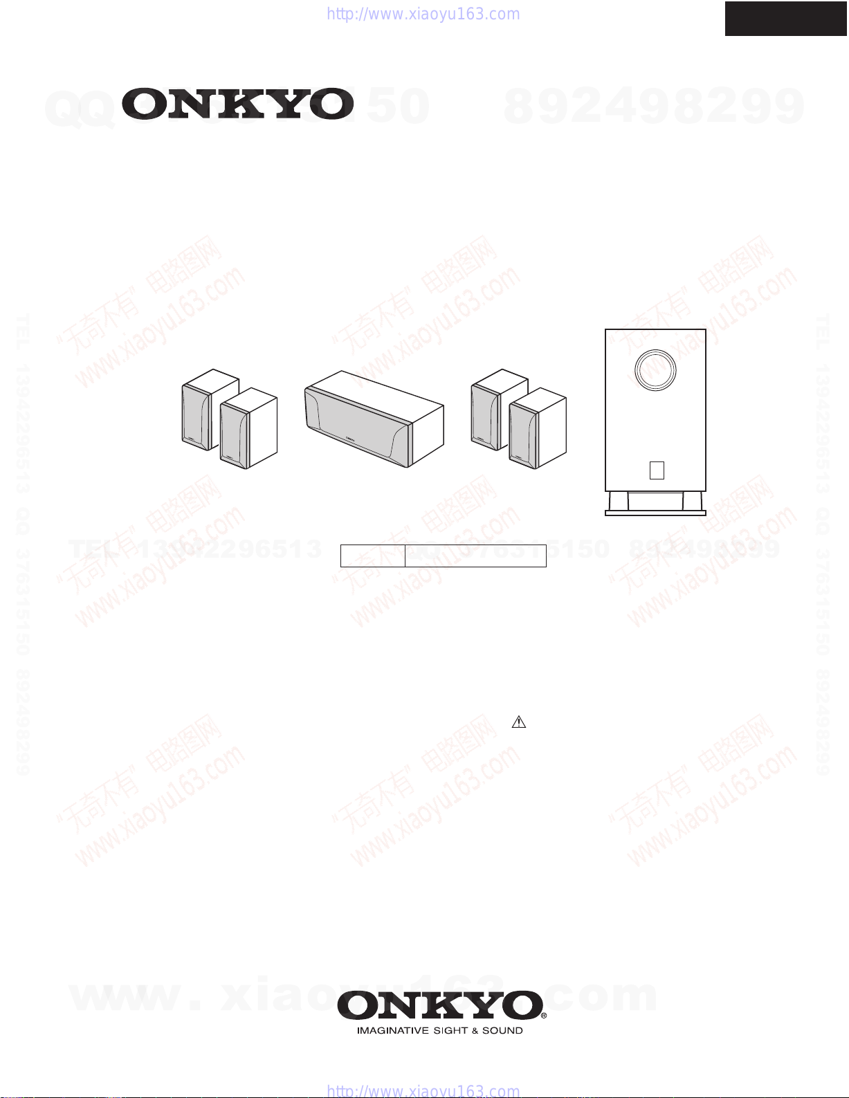
5.1-CH HOME THEATER SPEAKER PACKAGE
5
MODEL SKS-HT320(S)
1
5
0
8
9
2
4
9
SKS-HT320
Ref. No. 3846
092004
2
8
9
9
TEL 13942296513 QQ 376315150 892498299
TEL
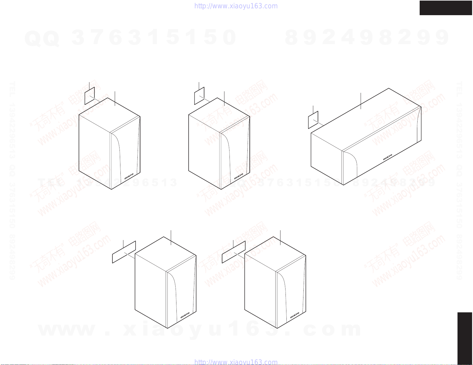
Front Speakers (L / R)
"SKF-320F"
13942296513
Center Speaker
"SKC-320C"
Silver model
Q
SAFETY-RELATED COMPONENT
WARNING!!
COMPONENTS IDENTIFIED BY MARK ON THE
SCHEMATIC DIAGRAM AND IN THE PARTS LIST ARE
CRITICAL FOR RISK OF FIRE AND ELECTRIC SHOCK.
REPLACE THESE COMPONENTS WITH ONKYO
PARTS WHOSE PART NUMBERS APPEAR AS SHOWN
IN THIS MANUAL.
MAKE LEAKAGE-CURRENT OR RESISTANCE
MEASUREMENTS TO DETERMINE THAT EXPOSED
PARTS ARE ACCEPTABLY INSULATED FROM THE
SUPPLY CIRCUIT BEFORE RETURNING THE
APPLIANCE TO THE CUSTOMER.
Surround Speakers (L / R)
3
Q
120 V AC, 60HzSMDD
"SKM-320S"
3
6
7
1
5
1
Powered Subwoofer
"SKW-320X"
8
0
5
9
2
4
9
8
2
9
TEL 13942296513 QQ 376315150 892498299
9
w
w
w
.
xia
o
y
u
1
6
3
.
c
o
m
Page 2
SPECIFICATIONS
SKS-HT320
7
Q
Q
TEL 13942296513 QQ 376315150 892498299
3
Powered Subwoofer (SKW-320X) Center Speaker (SKC-320C)
Type :
Input sensitivity / impedance :
Maximum output power :
Frequency response :
Cabinet capacity :
Dimensions (W x H x D) :
Weight :
Speaker unit :
Power supply :
Power consumption :
Other :
6
3
1
5
1
Powered Bass-reflex
220 mV / 15 k ohm
100 W (Dynamic Power)
35 Hz - 150 Hz
0.91 cubic feet (26 Litter)
9-1/16 x 17-13/16 x 15-7/8
inch
(230 x 436 x 404 mm)
24.7 lbs. (11.2 kg)
8 inch Cone
AC 120 V, 60 Hz
75 W
Auto-Standby function
5
0
Type :
Impedance :
Maximum input power :
Output sound pressure level :
Frequency response :
Crossover frequency :
Cabinet capacity :
Dimensions (W x H x D) :
Weight :
Speaker unit :
Woofer
Tweeter
Terminal :
Other :
8
9
2
4
8
9
2 Way Bass-reflex
8 ohm
100 W
78 dB/W/m
70 Hz - 50 kHz
4.5 kHz
0.057 cubic feet (1.6 Litter)
10-3/8 x 4 x 4-15/16 inch
(264 x 101 x 126 mm)
4.4 lbs. (2.0 kg)
3-1/8 inch Cone x 2
1 inch Balanced Dome
Spring type Color coded
Magnetic shielding
2
9
9
TEL 13942296513 QQ 376315150 892498299
TEL
13942296513
Front Speaker (SKF-320F)
Type :
Impedance :
Maximum input power :
Output sound pressure level :
Frequency response :
Crossover frequency :
Cabinet capacity :
Dimensions (W x H x D) :
Weight :
Speaker unit :
Woofer :
Tweeter :
Terminal :
Other :
2 Way Bass-reflex
8 ohm
100 W
76 dB/W/m
70 Hz - 50 kHz
4.5 kHz
0.035 cubic feet (1.0 Litter)
4 x 6-5/8 x 4-15/16 inch
(101 x 169 x 126 mm)
2.6 lbs. (1.2 kg)
3-1/8 inch Cone
1 inch Balanced Dome
Spring type Color coded
Magnetic shielding
Q
Q
4
2
9
8
0
5
1
5
1
3
6
7
3
Surround Speaker (SKM-320S)
Type :
Impedance :
Maximum input power :
Output sound pressure level :
Frequency response :
Crossover frequency :
Cabinet capacity :
Dimensions (W x H x D) :
Weight :
Speaker unit :
Woofer :
Tweeter :
Terminal :
Specifications and appearance are subject to change
without prior notice.
2 Way Bass-reflex
8 ohm
100 W
79 dB/W/m
70 Hz - 30 kHz
10 kHz
0.035 cubic feet (1.0 Litter)
4 x 6-5/8 x 4-15/16 inch
(101 x 169 x 126 mm)
1.8 lbs. (0.8 kg)
3-1/8 inch Cone Woofer
3/4 inch Ceramic Tweeter
Spring type Color coded
9
8
2
9
9
w
w
w
.
xia
o
y
u
1
6
3
.
c
o
m
Page 3
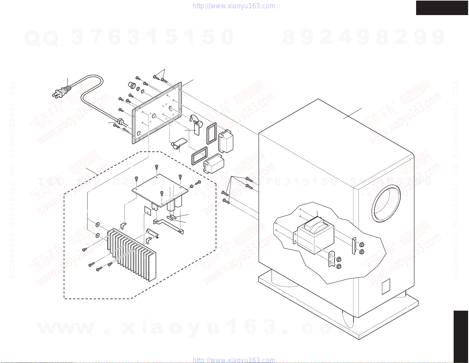
SKS-HT320
EXPLODED VIEWS-1
Q
TEL 13942296513 QQ 376315150 892498299
Q
SKW-320X : POWERED SUBWOOFER
TEL
3
A02
7
U01
13942296513
A03
6
3
1
5
SP06
x 10 pcs.
U03
U02
1
F903
F902
5
A01
0
A05 x 4 pcs.
Q
Q
3
7
6
8
3
1
9
5
1
A04
2
5
4
0
9
Refer to "EXPLODED VIEWS-2"
8
9
2
8
4
9
2
8
2
9
9
9
TEL 13942296513 QQ 376315150 892498299
9
w
<Note>
IC501---> Refer to "PRINTED CIRCUIT BOARD PARTS LIST"
w
w
.
x
i
a
o
y
u
1
6
3
.
c
o
SKS-HT320
m
Page 4
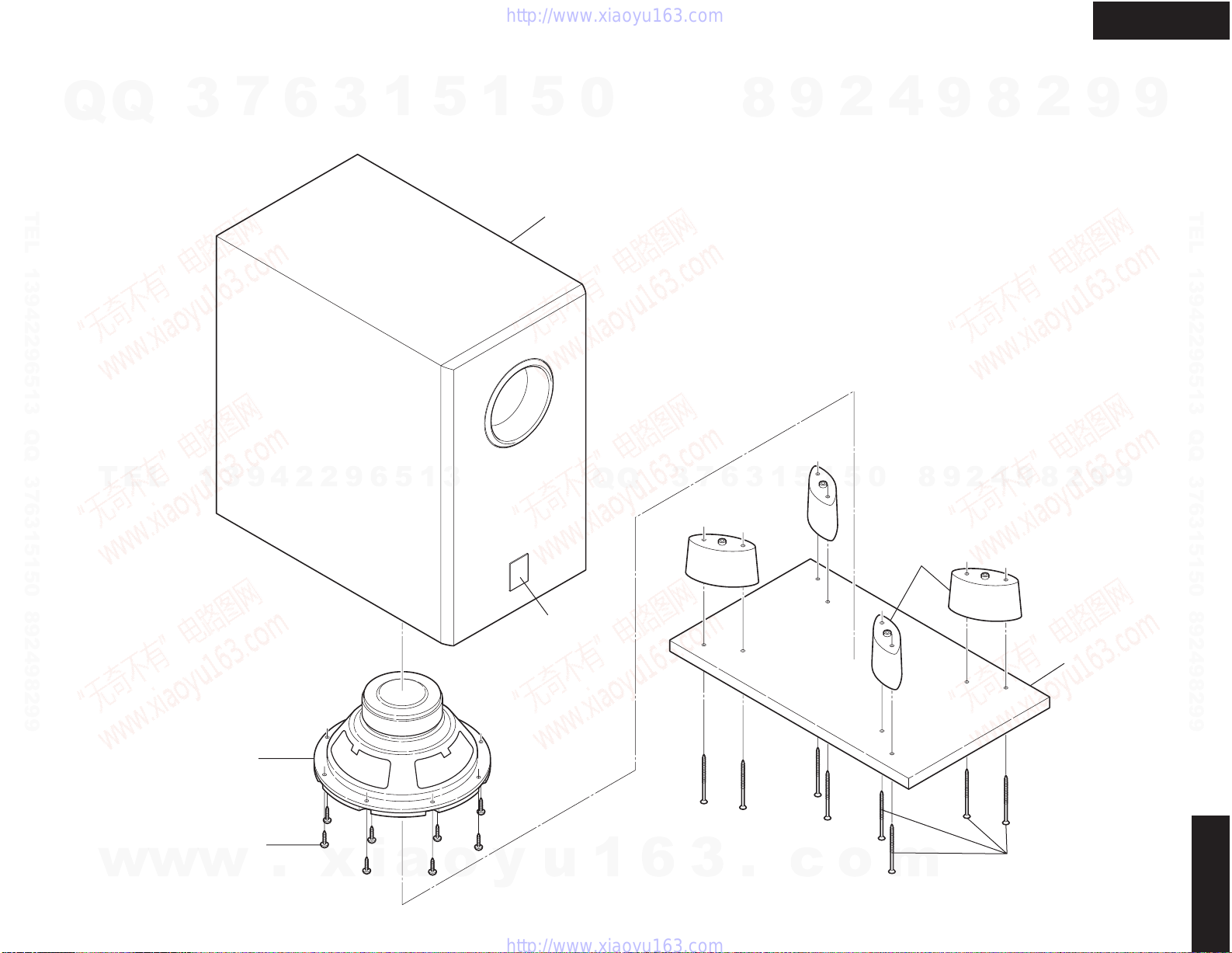
SKS-HT320
EXPLODED VIEWS-2
Q
TEL 13942296513 QQ 376315150 892498299
Q
SKW-320X : POWERED SUBWOOFER
TEL
3
7
13942296513
6
3
1
5
1
5
SP01
0
Q
Q
3
7
6
8
3
1
9
5
1
2
5
0
4
8
SP02
x 4 pcs.
9
9
2
8
4
9
2
8
2
9
9
9
TEL 13942296513 QQ 376315150 892498299
9
w
w
SP08
SP06
x 8 pcs.
w
.
x
i
a
o
SP04
y
u
1
6
3
.
c
o
m
SP03
SKS-HT320
SP05
x 8 pcs.
Page 5
SKS-HT320
EXPLODED VIEWS-3
Q
TEL 13942296513 QQ 376315150 892498299
Q
SKF-320F / SKC-320C / SKM-320S
TERMINAL :
White / Black
TEL
3
7
SP11
13942296513
"SKF-320F (L)" "SKF-320F (R)"
6
SP10 SP12
3
1
5
TERMINAL :
Red / Black
1
SP13
5
0
Q
Q
3
8
TERMINAL :
Green / Black
6
7
3
1
9
SP15
5
1
2
5
4
SP14
0
8
"SKC-320C"
9
9
2
8
4
9
2
8
2
9
9
9
TEL 13942296513 QQ 376315150 892498299
9
w
w
w
SP16 SP18
SP17 SP19
TERMINAL :
Blue / Black
.
x
NOT MAGNETICALLY SHIELDED NOT MAGNETICALLY SHIELDED
i
a
o
y
u
TERMINAL :
Gray / Black
1
6
SKS-HT320
3
"SKM-320S (R)""SKM-320S (L)"
.
c
o
m
Page 6
HTP-320
Q
TEL 13942296513 QQ 376315150 892498299
Q
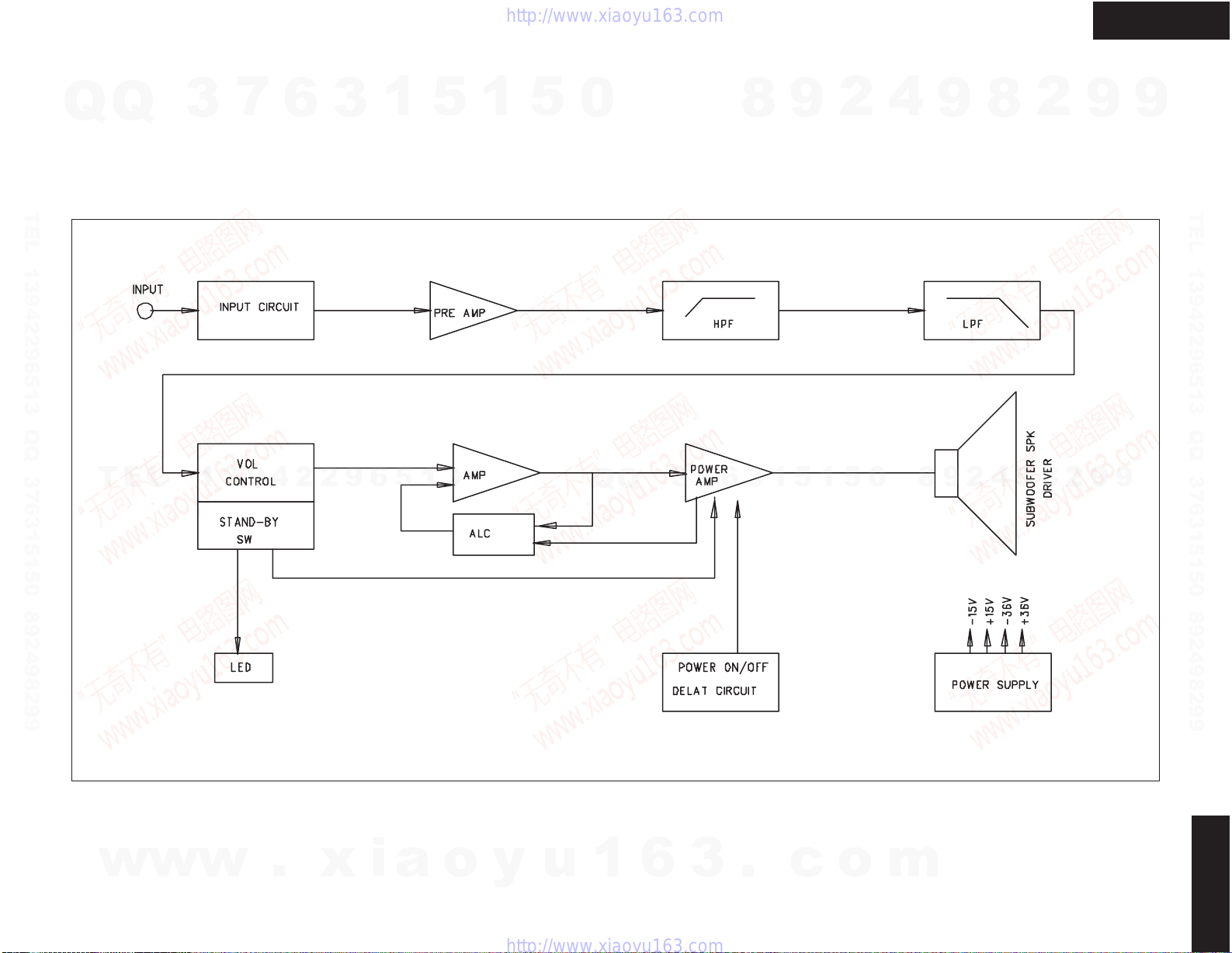
BLOCK DIAGRAM
SKW-320 : POWERED SUBWOOFER
TEL
3
7
13942296513
6
3
1
5
1
5
0
Q
Q
3
7
6
8
3
1
9
5
1
2
5
0
4
8
9
9
2
8
4
9
2
8
2
9
9
9
TEL 13942296513 QQ 376315150 892498299
9
w
w
w
.
x
i
a
o
y
u
1
6
3
.
c
o
HTP-320
m
Page 7
Q
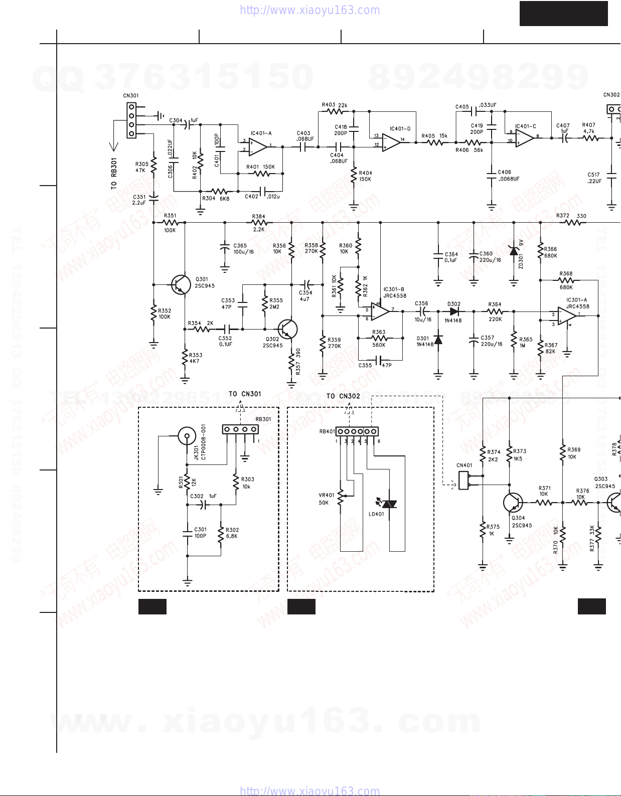
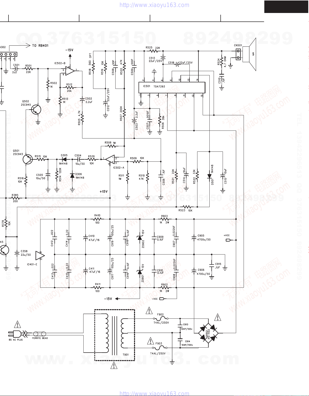
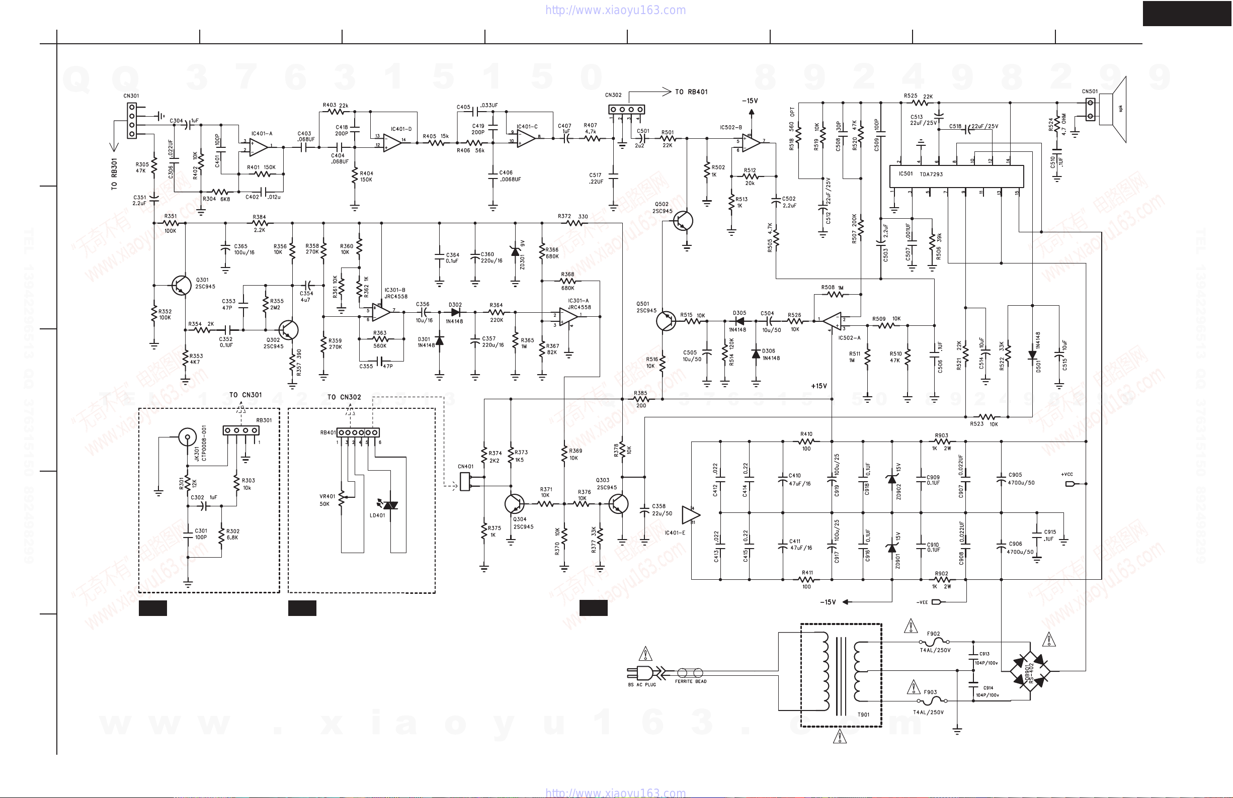
SCHEMATIC DIAGRAM
SKW-320: POWERED SUBWOOFER
Q
3
7
6
3
1
5
1
5
0
8
9
2
4
9
8
HT-320FGH
2
9
9
TEL 13942296513 QQ 376315150 892498299
TEL
13942296513
Q
Q
3
7
6
3
1
5
1
LINE
0
5
INPUT
8
9
2
4
9
8
2
9
TEL 13942296513 QQ 376315150 892498299
9
OUTPUT
LEVEL
w
w
w
.
xia
o
y
u
1
6
3
.
U02
c
INPUT PC BOARD
o
m
VR / LED PC BOARD
U03
Page 8
HTP-320
7
Q
Q
TEL 13942296513 QQ 376315150 892498299
3
6
3
1
5
1
5
0
8
9
2
4
9
8
2
9
SPEAKER
9
TEL 13942296513 QQ 376315150 892498299
TEL
MAIN PC BOARD
13942296513
Q
Q
3
7
6
3
1
5
1
5
0
8
9
2
4
9
8
2
9
9
w
w
w
.
xia
o
y
u
1
6
3
.
c
o
m
Page 9
HTP-320
A
SCHEMATIC DIAGRAM
SKW-320: POWERED SUBWOOFER
Q
1
TEL 13942296513 QQ 376315150 892498299
2
Q
3
7
BCDEFGH
6
3
1
5
1
5
0
8
9
2
4
9
8
2
9
9
SPEAKER
TEL 13942296513 QQ 376315150 892498299
T
E
3
4
5
L
LINE
INPUT
U02
1
3
9
INPUT PC BOARD
4
2
2
9
6
OUTPUT
LEVEL
LED
RED : STANDBY
GREEN : ON
VR / LED PC BOARD
U03
5
1
3
Q
U01
AC 120V / 60Hz
Q
MAIN PC BOARD
3
7
6
3
1
5
1
5
0
8
9
2
4
9
8
2
9
9
w
w
w
.
x
i
a
o
y
u
1
6
3
.
c
o
m
Page 10
HTP320
Q
TEL 13942296513 QQ 376315150 892498299
Q
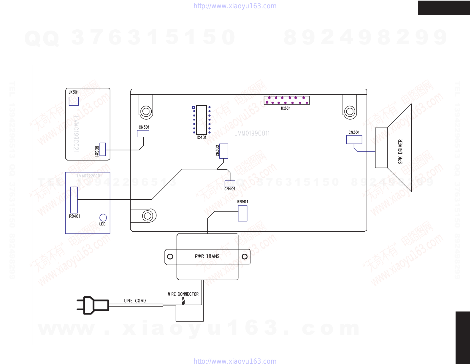
PC BOARD CONNECTION DIAGRAM
SKW-320 : POWERED SUBWOOFER
TEL
3
INPUT PC BOARD
7
13942296513
6
3
1
5
1
5
0
Q
Q
8
MAIN PC BOARD
1
3
6
7
3
9
5
1
2
5
0
4
8
9
9
2
8
4
9
2
8
2
9
9
9
TEL 13942296513 QQ 376315150 892498299
9
w
VR / LED PC BOARD
w
w
.
x
i
a
o
y
u
1
6
3
.
c
o
HTP-320
m
Page 11
HTP-320
A
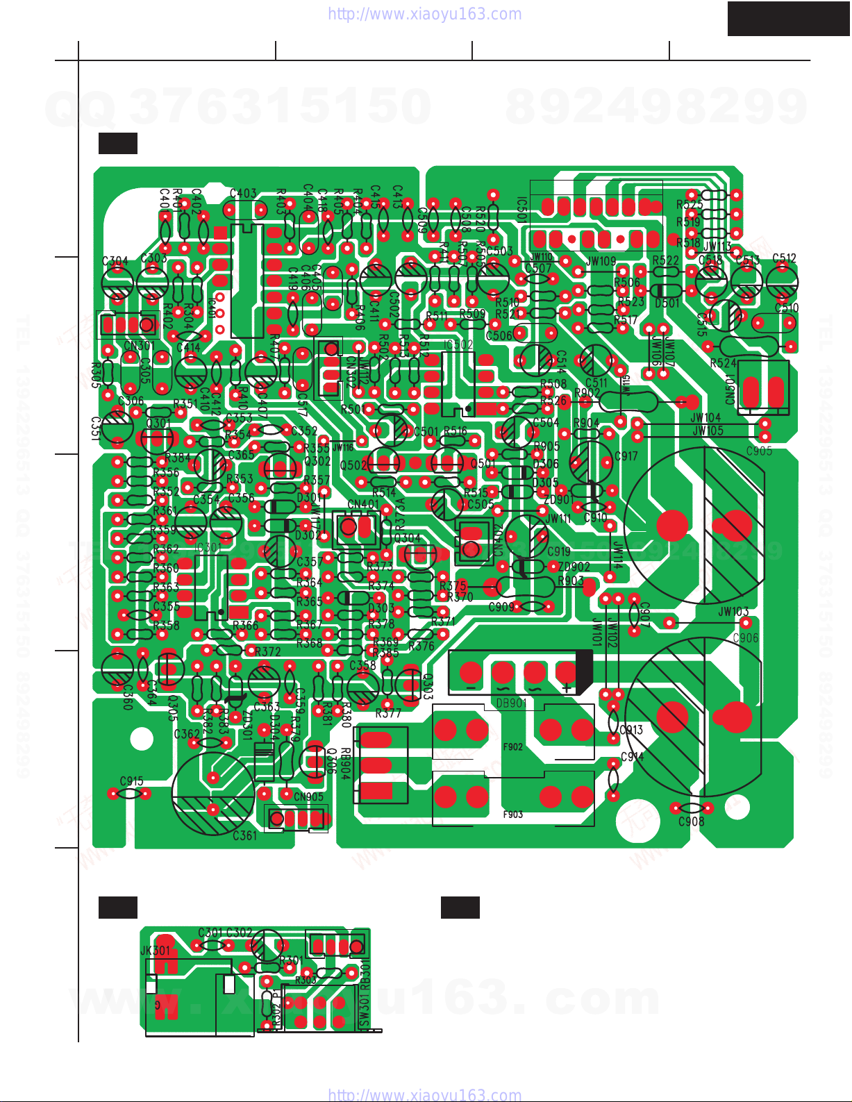
PRINTED CIRCUIT BOARD VIEW
SKW-320POWERED SUBWOOFER
Q
Q
U01
1
TEL 13942296513 QQ 376315150 892498299
2
7
3
MAIN PC BOARD
6
3
1
5
BCD
1
5
0
8
9
2
4
9
8
2
9
9
TEL 13942296513 QQ 376315150 892498299
TEL
3
4
5
13942296513
INPUT PC BOARD
U02
Q
Q
0
5
1
5
1
3
6
7
3
VR / LED PC BOARD
U03
No PC board view
Look over the actual PC board on hand
8
9
2
4
9
8
2
9
9
w
w
w
.
xia
o
y
u
1
6
3
.
c
o
m
Page 12
Q
Q
3
7
®
6
3
1
5
1
5
0
120V - 100W DMOS AUDIO AMPLIFIER WITH MUTE/ST-BY
VERY HIG H OPERATI NG VOLTAGE R ANGE
(±50V)
DMOS POWER STAGE
HIGH OUTPUT POWER (100W @ THD =
TEL 13942296513 QQ 376315150 892498299
TEL
10%, R
MUTING/STAND- BY FUNC TION S
NO SWITCH ON/OFF NOISE
VERY LOW DISTORTION
VERY LOW NOISE
SHORT CIRCUIT PROTECTED (WITH NO IN-
PUT SIGNAL APPLIED)
THERMAL SHUTDOWN
CLIP DETECTOR
MODULARITY (MORE DEVICES CAN BE
EASILY CONNECTED IN PARALLEL TO
DRIVE VERY LOW IMPEDANCES)
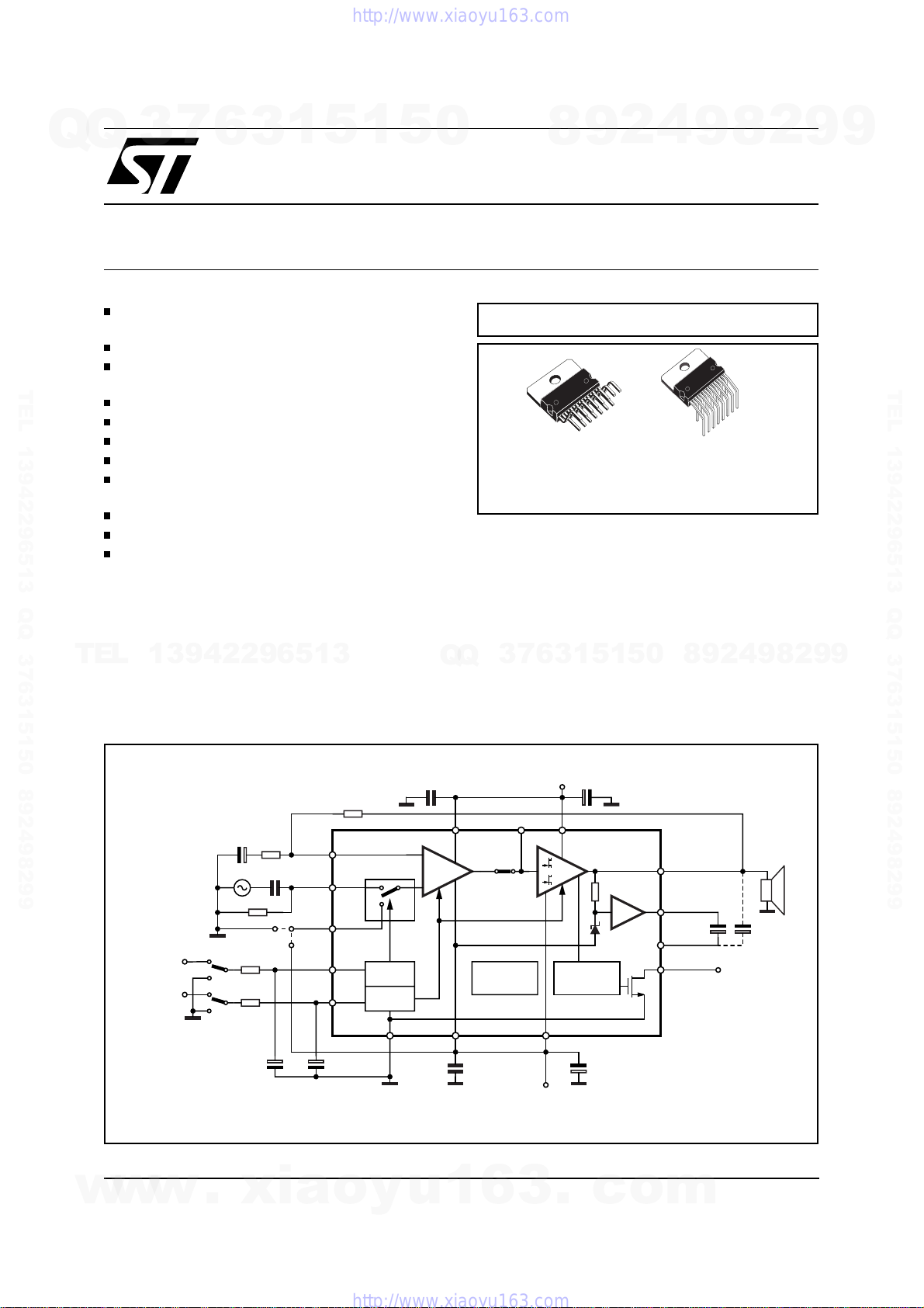
DESCRIPTION
The TDA7293 is a monolithic integrated circuit in
Multiwatt15 package, intended for use as audio
class AB amplifier in Hi-Fi field applications
(Home Stereo, self powered loudspeakers, Top-
L
= 8Ω, VS = ±40V)
13942296513
Q
Q
MULTIPOWER BCD TECHNOLOGY
Multiwatt15V Multiwatt15H
TDA7293V TDA7293HS
class TV). Thanks to the wide voltage range and
to the high out current c apability it is able to supply the highest power into both 4Ω and 8Ω loads.
The built in muting function with turn on delay
simplifies the remote operation avoiding switching
on-off noises.
Parallel mode is made possible by connecting
more device through of pin11. High out put power
7
3
can be delivered to very low impedance loads, so
optimizing the thermal dissipation of the system.
2
9
8
ORDERING NUMBERS:
5
1
5
1
3
6
4
9
TDA7293
2
9
8
0
8
4
2
9
8
9
2
9
9
TEL 13942296513 QQ 376315150 892498299
9
Figure 1: Typical Application and Test Circuit
R3 22K
C2
R2
22µF
VMUTE
VSTBY
January 2003
680Ω
C1 470nF
R1 22K
R5 10K
R4 22K
C3 10µF C4 10µF
IN- 2
IN+
3
4
SGND
(**)
10
MUTE
9
STBY
(*) see Application note
(**) for SLAVE function
MUTE
STBY
1
STBY-GND
C7 100nF C6 1000µF
BUFFER DRIVER
11
713
-
+
THERMAL
SHUTDOWN
-Vs -PWVs
C9 100nF C8 1000µF
+Vs
PROTECTION
158
-Vs
+PWVs+Vs
S/C
14
12
6
5
D97AU805A
OUT
BOOT
LOADER
C5
22µF
BOOTSTRAP
CLIP DET
(*)
VCLIP
1/15
w
w
w
.
xia
o
y
u
1
6
3
.
c
o
m
Page 13
Q
TDA7293
7
Q
3
PIN CONNECTION (Top view)
6
3
1
5
1
5
0
8
9
2
4
9
8
2
9
9
15
14
13
12
11
10
9
8
7
6
TEL 13942296513 QQ 376315150 892498299
TAB CONNECTED TO PIN 8
ABSOLUTE MAXIMUM RATINGS
Symbol Parameter Value Unit
Supply Voltage (No Signal)
S
V
1
13942296513
2
3
4
5
6
9
, TjStorage and Junction Temperature 150
STAND-BY
Input Voltage (inverting) Referred to -VS 90 V
Maximum Differential Inputs
3
Input Voltage (non inverting) Referred to -VS 90 V
Signal GND Voltage Referred to -VS 90 V
Clip Detector Voltage Referred to -VS 120 V
Bootstrap Voltage Referred to -VS 120 V
Stand-by Voltage Referred to -VS 120 V
Mute Voltage Referred to -VS 120 V
Buffer Voltage Referred to -VS 120 V
Bootstrap Loader Voltage Referred to -VS 100 V
Output Peak Current 10 A
Power Dissipation T
Operating Ambient Temperature Range 0 to 70
GND Voltage Referred to -VS (pin 8) 90 V
= 70°C50W
case
TEL
V
V
V
- V
V
2
V
V
V
V
V
V
10
V
11
V
12
I
O
P
tot
T
op
T
stg
5
4
3
2
1
D97AU806
Q
Q
-VS (POWER)
OUT
+V
BOOTSTRAP LOADER
BUFFER DRIVER
MUTE
STAND-BY
-V
+V
BOOTSTRAP
CLIP AND SHORT CIRCUIT DETECTOR
SIGNAL GROUND
NON INVERTING INPUT
INVERTING INPUT
STAND-BY GND
7
3
(POWER)
S
(SIGNAL)
S
(SIGNAL)
S
3
6
1
5
1
60 V
±
8
0
5
30 V
±
9
2
4
9
8
°
°
TEL 13942296513 QQ 376315150 892498299
9
9
2
C
C
THERMAL DATA
Symbol Description
Thermal Resistance Junction-case 1 1.5
w
.
xia
o
2/15
w
w
R
th j-case
y
u
1
6
3
.
c
Typ
o
m
Max Unit
C/W
°
Page 14
7
Q
Q
TEL 13942296513 QQ 376315150 892498299
TEL
3
ELECTRICAL CHARACTERISTICS (Refer to the Test Circuit V
T
= 25°C, f = 1 kHz; unless otherwise specified).
amb
Symbol Parameter Test Condition Min. Typ. Max. Unit
V
S
I
q
I
b
V
OS
I
OS
P
O
d Total Harmonic Distortion (**) PO = 5W; f = 1kHz
I
SC
SR Slew Rate 5 10 V/µs
G
V
G
V
e
N
R
i
SVR Supply Voltage Rejection f = 100Hz; V
T
S
STAND-BY FUNCTION
V
ST on
13942296513
V
ST off
ATT
st-by
I
q st-by
MUTE FUNCTION
V
Mon
V
Moff
ATT
mute
CLIP DETECTOR
Duty Duty Cycle ( pin 5) THD = 1% ; RL = 10KΩ to 5V 10 %
I
CLEAK
SLAVE FUNCTION pin 4
V
Slave
V
Master
Note (1):
Note:
Note (**):
Vmin
G
Pin 11 only for modular connection. Max external load 1MΩ/10 pF, only for test purpose
Tested with optimized Application Board (see fig. 2)
6
Supply Range
Quiescent Current 50 100 mA
Input Bias Current 0.3 1
Input Offset Voltage -10 10 mV
Input Offset Current 0.2
RMS Continuous Output Power d = 1%:
Current Limiter Threshold VS ≤ ± 40V 6.5 A
Open Loop Voltage Gain 80 dB
Closed Loop Voltage Gain (1) 29 30 31 dB
Total Input Noise A = curve
Input Resistance 100 k
Thermal Protection DEVICE MUTED 150
Stand-by on Threshold 1.5 V
Stand-by off Threshold 3.5 V
Stand-by Attenuation 70 90 dB
Quiescent Current @ Stand-by 0.5 1 mA
(Ref: to pin 1)
Mute on Threshold 1.5 V
Mute off Threshold 3.5 V
Mute AttenuatIon 60 80 dB
SlaveThreshold 1V
Master Threshold 3 V
26dB
≥
1
3
(Ref: to pin 1)
(Ref: to pin 8 -V
5
1
5
0
R
= 4
VS = ± 29V,
Ω;
L
d = 10%
= 4Ω ; VS = ±29V
R
L
P
= 0.1 to 50W; f = 20Hz to 15kHz
O
f = 20Hz to 20kHz
= 0.5Vrms 75 dB
ripple
DEVICE SHUT DOWN 160
7
3
Q
Q
THD = 10% ;
RL = 10KΩ to 5V
PO = 50W 3
)
S
4
2
9
8
= ±40V, RL = 8Ω, Rg = 50 Ω;
S
12
±
75 80
90 100
0
5
1
5
1
3
6
30 40 50 %
9
80
100
0.005
1
310
9
8
TDA7293
8
50 V
±
0.1
4
2
2
9
9
A
µ
A
µ
W
W
%
%
V
µ
V
µ
Ω
C
°
C
°
2
8
A
µ
9
9
TEL 13942296513 QQ 376315150 892498299
9
w
w
w
.
xia
o
y
u
1
6
3
.
c
o
3/15
m
Page 15
Q
TDA7293
7
Q
3
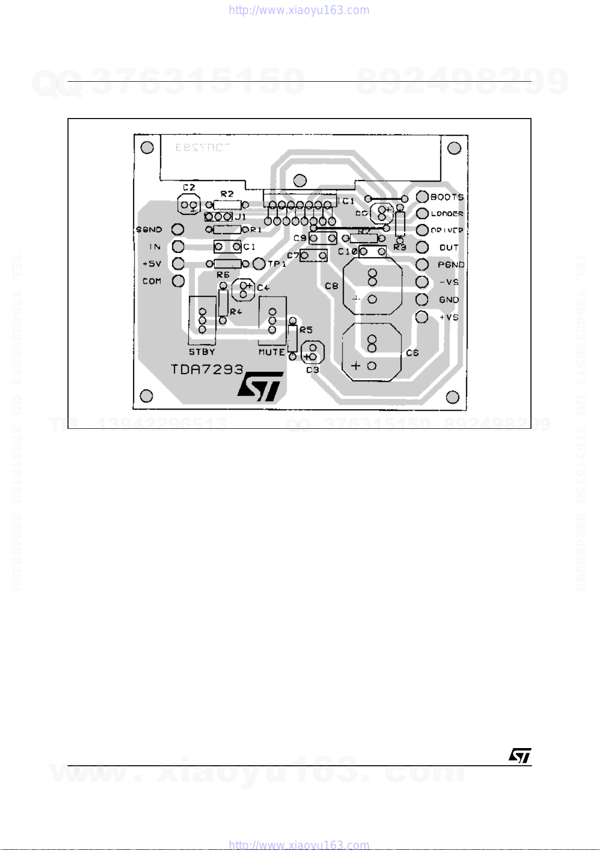
Figure 2: Typical Application P.C. Board and Component Layout (scale 1:1)
6
3
1
5
1
5
0
8
9
2
4
9
8
2
9
9
TEL 13942296513 QQ 376315150 892498299
TEL
13942296513
Q
Q
3
7
6
3
1
5
1
5
0
8
9
2
4
9
8
2
9
TEL 13942296513 QQ 376315150 892498299
9
4/15
w
w
w
.
xia
o
y
u
1
6
3
.
c
o
m
Page 16
Q
TDA7293
7
Q
3
APPLICATION SUGGES TION S (see Test and Application Circuits of the Fig. 1)
The recommended values of t he external components are t hose shown on t he application circuit o f Fig-
ure 1. Different values can be used; the following table can help the designer.
6
3
1
5
1
5
0
8
9
2
4
9
8
2
9
9
COMPONENTS SUGGESTED VALUE PURPOSE
R1 (*) 22k INPUT RESISTANCE INCREASE INPUT
R2 680
R3 (*) 22k INCREASE OF GAIN DECREASE OF GAIN
TEL 13942296513 QQ 376315150 892498299
TEL
R4 22k ST-BY TIME
R5 10k MUTE TIME
C1 0.47µF INPUT DC
C2 22µF FEEDBACK DC
C3 10µF MUTE TIME
C4 10µF ST-BY TIME
13942296513
Ω
CLOSED LOOP GAIN
SET TO 30dB (**)
CONSTANT
CONSTANT
DECOUPLING
DECOUPLING
CONSTANT
Q
3
CONSTANT
Q
7
LARGER THAN
SUGGESTED
IMPEDANCE
DECREASE OF GAIN INCREASE OF GAIN
LARGER ST-BY
ON/OFF TIME
LARGER MUTE
ON/OFF TIME
LARGER MUTE
ON/OFF TIME
LARGER ST-BY
5
1
3
6
ON/OFF TIME
1
5
0
SMALLER THAN
SUGGESTED
DECREASE INPUT
IMPEDANCE
SMALLER ST-BY
ON/OFF TIME;
POP NOISE
SMALLER MUTE
ON/OFF TIME
HIGHER LOW
FREQUENCY
CUTOFF
HIGHER LOW
FREQUENCY
CUTOFF
SMALLER MUTE
ON/OFF TIME
SMALLER ST-BY
2
9
8
ON/OFF TIME;
POP NOISE
4
9
8
2
9
TEL 13942296513 QQ 376315150 892498299
9
C5 22µFXN (***) BOOTSTRAPPING SIGNAL
C6, C8 1000µF SUPPLY VOLTAGE
C7, C9 0.1µF SUPPLY VOLTAGE
(*) R1 = R3 for pop optimization
(**) Closed Loop Gain has to be ≥ 26dB
(***) Multiplay this value for the number of modular part connected
D98AU821
S
)
Slave function: pin 4 (Ref to pin 8 -V
+3V
-V
S
-V
+1V
S
-V
S
MASTER
UNDEFINED
SLAVE
DEGRADATION AT
LOW FREQUENCY
BYPASS
BYPASS
Note:
If in the application, the speakers are connected
via long wires, it is a good rule to add between
the output and GND, a Boucherot Cell, in order to
avoid dangerous spurious oscillations when the
speakers terminal are shorted.
The suggested Boucherot Resistor is 3.9Ω/2W
and the capacitor is 1µF.
DANGER OF
OSCILLATION
w
w
w
.
xia
o
y
u
1
6
3
.
c
o
5/15
m
Page 17

TDA7293
7
Q
Q
TEL 13942296513 QQ 376315150 892498299
TEL
3
INTRODUCTION
In consumer electronics, an increasing demand
has arisen for very high power monolithic audio
amplifiers able to match, with a low cost, the performance obtained from the best discrete designs.
The task of realizing this linear integrated circuit
in conventional bipolar technology is made extremely difficult by the occurence of 2nd breakdown phoenomenon. It limits the safe operating
area (SOA) of the power devices, and, as a consequence, the maximum attainable output power,
especially in presence of highly reactive loads.
Moreover, full exploitation of the SOA translates
into a substantial increase in circuit and layout
complexity due to the need of sophisticated protection circuits.
To overcome these substantial drawbacks, the
use of power MOS devices, which are immune
from secondary breakdown is highly desirable.
The device described has therefore been developed in a mixed bipolar-MOS high voltage technology called BCDII 100/120.
1) Output Stage
The main design task in developping a po wer operational amplifier, independently of the technology used, is that of realization of the output stage.
The solution shown as a principle shematic by
13942296513
Fig3 represents the DMOS unity - gain output
buffer of the TDA7293.
This large-signal, high-power buffer must be capable of handling extremely high current and voltage levels while maintaining acceptably low harmonic distortion and good behaviour over
6
3
1
5
1
5
0
frequency response; moreover, an accurate control of quiescent current is required.
A local linearizing feedback, provided by differential amplifier A, is used to fullfil the above requirements, allowing a simple and effective quiescent
current setting.
Proper biasing of the power output transistors
alone is however not enough to guarantee the absence of crossover distortion.
While a linearization of the DC transfer characteristic of the stage is obtained, the dynamic behaviour of the system must be taken into account.
A significant aid in keeping the distortion contributed by the final stage as low as possible is provided by the compensation scheme, which exploits the direct connection of the Miller capacitor
at the amplifier’s output to introduce a local AC
feedback path enclosing the output stage itself.
2) Protections
In designing a power IC, particular attention must
be reserved to the circuits devoted to protection
of the device from short circuit or overload conditions.
Due to the absence of the 2nd breakdown phenomenon, the SOA of the power DMOS tr ansistors is delimited only by a maximum dissipation
curve dependent on the duration of the applied
stimulus.
7
3
Q
Q
In order to fully exploit the capabilities of the
power transistors, the protection scheme implemented in this device combines a conventional
SOA protection circuit with a novel local temperature sensing technique which " dynamically" controls the maximum dissipation.
8
6
3
9
1
5
2
1
5
4
0
9
8
9
8
2
4
2
9
8
9
2
9
9
TEL 13942296513 QQ 376315150 892498299
9
Figure 3: Principle Schematic of a DMOS unity-gain buffer.
6/15
w
w
w
.
xia
o
y
u
1
6
3
.
c
o
m
Page 18

7
Q
Q
TEL 13942296513 QQ 376315150 892498299
3
Figure 4: Turn ON/OFF Suggested Sequence
6
3
1
+Vs
(V)
+40
-40
-Vs
V
IN
(mV)
V
ST-BY
PIN #9
(V)
5
5V
1
5
0
8
9
2
4
9
TDA7293
2
8
9
9
TEL 13942296513 QQ 376315150 892498299
V
MUTE
PIN #10
(V)
I
Q
(mA)
V
OUT
(V)
TEL
13942296513
In addition to the overload protection described
above, the device features a thermal shutdown
circuit which initially puts the device into a muting
state (@ Tj = 150
Tj = 160
Full protection against electrostatic discharges on
every pin is included.
Figure 5: Single Signal ST-BY/MUTE Control
3) Other Features
The device is provided with both stand-by and
MUTE/
ST-BY
o
C).
Circuit
o
C) and then into stand-by (@
20K
10K 30K
1N4148
5V
OFF
ST-BY
MUTE STBY
PLAY
MUTE MUTE
10µF10µF
D93AU014
Q
Q
mute functions, independently driven by two
CMOS logic compatible input pins.
The circuits dedicated to the switching on and off
of the amplifier have been carefully optimized to
avoid any kind of uncontrolled audible transient at
the output.
The sequence that we recommend during the
ON/OFF transients is shown by Figure 4.
The application of figure 5 shows the possibility of
using only one command for both st-by and mute
functions. On both the pins, the maximum applicable range corresponds to the oper ating supply
voltage.
APPLICATION INFORMATION
HIGH-EFFICIENCY
Constraints of implementing high power solutions
are the power dissipation and the size of the
power supply. These are both due to the low efficiency of conventional AB class amplifier approaches.
Here below (figure 6) is described a circuit proposal for a high efficiency amplifier which can be
adopted for both HI-FI and CAR-RADIO applications.
3
7
ST-BY OFF
5
1
3
6
D98AU817
1
5
0
8
9
2
4
9
8
2
9
9
w
w
w
.
xia
o
y
u
1
6
3
.
c
o
7/15
m
Page 19

TDA7293
7
Q
Q
TEL 13942296513 QQ 376315150 892498299
TEL
3
The TDA7293 is a monolithic MOS power amplifier which can be operated at 100V supply voltage
(120V with no signal applied) while delivering output currents up to ±6.5 A.
This allows the use of this device as a very high
power amplifier (up to 180W as peak power with
T.H.D.=10 % and Rl = 4 Ohm); the only drawback
is the power dissipation, hardly manageable in
the above power range.
The typical junction-to-case thermal resistance of
the TDA7293 is 1
avoid that, in worst case conditions, the chip temperature exceedes 150
of the heatsink must be 0.038
bient temperature of 50
As the above value is pratically unreachable; a
high efficiency system is needed in those cases
where the continuous RMS output power is higher
than 50-60 W.
The TDA7293 was designed to work also in
higher efficiency way.
For this reason there are four power supply pins:
two intended for the signal part and two for the
power part.
T1 and T2 are two power transistors that only
operate when the output power reaches a certain
threshold (e.g. 20 W). If the output power increases, these transistors are switched on during
the portion of t he signal where more output voltage swing is needed, thus "bootstrapping" the
power supply pins (#13 and #15).
The current generators formed by T4, T7, zener
13942296513
diodes Z1, Z2 and resistors R7,R8 define the
minimum drop across the power MOS transistors
of the TDA7293. L1, L2, L3 and the snubbers C9,
R1 and C10, R2 stabilize the loops formed by the
"bootstrap" circuits and the output stage of the
TDA7293.
By considering again a maximum average
output power (music signal) of 20W, in case
of the high efficiency application, the thermal
resistance value needed from the heatsink is
o
C/W (Vs =±50 V and Rl= 8 Ohm).
2.2
All components (TDA7293 and power transistors T1 and T2) can be pl aced on a 1.5
heatsink, with the power darlingtons electrically
insulated from the heatsink.
Since the total power dissipation is less than that
of a usual class AB amplifier, additional cost savings can be obtained while optimizing the power
supply, even with a high heatsink .
BRIDGE APPLICATION
Another application suggestion is the BRIDGE
configuration, where two TDA7293 are used.
In this application, the value of the load must not
be lower than 8 Ohm for dissipation and current
capability reasons.
A suitable field of application includes HI-FI/TV
subwoofers realizations.
6
1
5
1
3
o
C/W (max= 1.5 oC/W). To
o
C, the thermal resistance
o
o
C).
C/W (@ max am-
5
o
C/W
0
The main advantages offered by this solution are:
- High power performances with limited supply
voltage level.
- Considerably high output power even with high
load values (i.e. 16 Ohm).
With Rl= 8 Ohm, Vs = ±25V the maximum output
power obtainable is 150 W, while with Rl=16
Ohm, Vs = ±40V the maximum Pout is 200 W.
APPLICATION NOTE: (ref. fig. 7)
Modular Application (more Devices in Parallel)
The use of the modular application lets very high
power be delivered to very low impedance loads.
The modular application implies one device to act
as a master and the others as slaves.
The slave power stages are driven by the master
devic e and work in parallel all together, whil e the input and the gain st ages of the slave device are disabled, t he figure below shows t he connectio ns required to co nfi g ure tw o dev ic es to w o rk toge the r.
The master chip connections are the same as
the normal single ones.
The outputs can be conne cted t ogether wi th-
out the need of any ballast resistance.
The slave SGND pin must be tied to the negative supply.
7
3
Q
Q
The slave ST-BY and MUTE pins must be connected to the master ST-BY and MUTE pins.
The bootstrap lines must be connected together and the bootstrap capacitor must be increased: for N devices the boostrap capacitor
must be 22µF times N.
The slave IN-pin must be connected to the
negative supply.
THE BOOTSTRAP CAPACITOR
For compatibility purpose with the previous devices of the family, the boostrap capacitor can be
connected both between the bootstrap pin (6) and
the output pin (14) or between the boostrap pin
(6) and the bootstrap loader pin (12).
When the bootcap is connected between pin 6
and 14, the maximum supply voltage in presence
of output signal is limited to 100V, due the bootstrap capacitor overvoltage.
When the bootcap is connected between pins 6
and 12 the maximum supply voltage extend to the
full voltage that the technology can stand: 120V.
This is accomplished by the clamp introduced at
the bootstrap loader pin (12): this pin follows the
output voltage up to 100V and remains clamped
at 100V for higher output voltages. This feature
lets the output voltage swing up to a gate-source
voltage from the positive supply (V
8
6
3
9
1
5
2
1
5
4
0
9
8
8
2
9
S
-3 to 6V).
4
2
9
8
9
2
9
9
TEL 13942296513 QQ 376315150 892498299
9
8/15
w
w
w
.
xia
o
y
u
1
6
3
.
c
o
m
Page 20

Q
7
Q
3
Figure 6: High Efficiency Application Circuit
6
3
1
5
1
5
0
8
9
2
4
9
TDA7293
2
8
9
9
+50V
D6
1N4001
PLAY
ST-BY
D5
1N4148
D1 BYW98100
INC7
D2 BYW98100
C12 330nF
R12
13K
C13 10µF
R13 20K
R14 30K
R15 10K
C14
10µF
Q
Q
3
4
TDA7293
9
1
10
7
3
815
+25V
R22
10K
R23
10K
C9
330nF
R1
2
R2
2
C10
C8
330nF
D7
1N4001
C1
63V
63V
C3
100nF
C2
C4
100nF
R20
1000µF
20K
TEL 13942296513 QQ 376315150 892498299
TEL
GND
R21
1000µF
20K
-25V
-50V
Figure 6a: PCB and Component Layout of the fig. 6
13942296513
C5
1000µF
35V
C6
1000µF
35V
100nF
100nF
137
6
BDX53A
R17 270
L1 1µH
14
12
L2 1µH
R19 270
BDX54A
3
T1
2
6
1
T3
BC394
D3 1N4148
R3 680
R16
13K
C15
22µF
D4 1N4148
T2
T6
BC393
5
1
5
C11 22µF
L3 5µH
R18 270
0
R4
270R5270
T4
BC393
Z1 3.9V
Z2 3.9V
T7
BC394
R9
270
8
R6
20K
R7
3.3K
R8
3.3K
R10
270
D97AU807C
9
2
T5
BC393
1.8nF
1.8nF
T8
BC394
R11
20K
4
C16
C17
9
OUT
8
P
2
TEL 13942296513 QQ 376315150 892498299
ot
9
9
w
w
w
.
xia
o
y
u
1
6
3
.
c
o
9/15
m
Page 21

Q
TDA7293
7
Q
3
Figure 6b: PCB - Solder Side of the fig. 6.
6
3
1
5
1
5
0
8
9
2
4
9
8
2
9
9
TEL 13942296513 QQ 376315150 892498299
Figure 7: Modular Application Circuit
+Vs
7
3
11
PROTECTION
158
-Vs
+Vs
11
PROTECTION
158
-Vs
TEL
13942296513
MASTER
C2
R2
22µF
680Ω
IN- 2
C1 470nF
IN+
R1 22K
SGND
VMUTE
VSTBY
SLAVE
R5 10K
R4 22K
MUTE
STBY
C4 10µF
C3 10µF
IN- 2
IN+ 3
SGND
MUTE
STBY
R3 22K
3
4
10
9
4
10
9
C7 100nF C6 1000µF
Q
Q
BUFFER
DRIVER
713
-
+
MUTE
STBY
1
STBY-GND
C7 100nF C6 1000µF
MUTE
STBY
1
STBY-GND
THERMAL
SHUTDOWN
-Vs -PWVs
C9 100nF C8 1000µF
BUFFER
DRIVER
713
-
+
THERMAL
SHUTDOWN
-Vs -PWVs
C9 100nF C8 1000µF
6
+PWVs+Vs
S/C
+PWVs+Vs
S/C
3
1
5
14
12
6
5
14
12
6
5
5
1
OUT
BOOT
LOADER
C5
47µF
BOOTSTRAP
CLIP DET
OUT
BOOT
LOADER
BOOTSTRAP
D97AU808D
0
C10
100nF
TEL 13942296513 QQ 376315150 892498299
9
9
2
8
9
4
2
9
8
R7
2Ω
10/15
w
w
w
.
xia
o
y
u
1
6
3
.
c
o
m
Page 22

Q
7
Q
3
Figure 8a: Modular Application P.C. Board and Component Layout (scale 1:1) (Component SIDE)
6
3
1
5
1
5
0
8
9
2
4
9
TDA7293
2
8
9
9
TEL 13942296513 QQ 376315150 892498299
TEL
13942296513
Figure 8b: Modular Application P.C. Board and Component Layout (scale 1:1) (Solder SIDE)
Q
Q
3
7
6
3
1
5
1
5
0
8
9
2
4
9
8
2
9
TEL 13942296513 QQ 376315150 892498299
9
w
w
w
.
xia
o
y
u
1
6
3
.
c
o
11/15
m
Page 23

TDA7293
7
Q
Q
TEL 13942296513 QQ 376315150 892498299
TEL
3
Figure 9: Distortion vs Output Power
T.H.D (%)
10
5
2
1
0.5
0.2
0.1
0.05
0.02
0.01
0.005
0.002
0.001
Figure 10: Distortion vs Output Power
T.H.D (%)
10
5
2
1
0.5
0.2
0.1
13942296513
0.05
0.02
0.01
0.005
0.002
0.001
Figure 11: Distortion vs Frequency
T.H.D. (%)
10
1
0.1
0.01
0.001
00.1110100
6
Vs = +/-29V
Rl = 4 Ohm
210051020 50
Vs = +/-40V
Rl = 8 Ohm
2 10051020 50
VS= +/- 35 V
Rl= 8 Ohm
Pout=100 mW
1
3
f = 1KHz
Pout (W)
f = 1KHz
Pou t (W)
Frequen cy (K Hz)
5
1
f = 20 KHz
f = 20 KHz
Po=50 W
5
0
Figure 12: Modular Application Derating Rload
6
5
4
3
2
1
Minimum Allovable Load (ohm)
0
20 25 30 35 40 45 50
Figure 13: Modular Application Pd vs Vsupply
60
50
40
30
7
3
Q
Q
20
Pdissipated (W)
10
0
20 25 30 35 40 45 50
Figure 14: Output Power vs. Supply Voltage
Po (W)
120
110
100
90
80
70
60
50
40
30
20
10
0
10 12 14 16 18 20 22 24 26 28 30 32 34 36 38 40
4
2
9
8
vs Vsupply (ref. fig. 7)
Forbidden A rea
Pd > 50W at T
Supply Voltage (+/-Vcc)
(ref. fig. 7)
Dissipated Power for each
device of the modular
application
3
6
5
1
Rl=8 Ohm
f= 1 KHz
4ohm
0
5
1
Supply Voltage (+/-Vcc)
8ohm
T.H.D.=10 %
Vs (+/-V)
8
9
case
=70°C
Pd limit at Tcase=70°C
4
2
9
8
THD=0.5 %
2
9
8
9
2
9
9
TEL 13942296513 QQ 376315150 892498299
9
12/15
w
w
w
.
xia
o
y
u
1
6
3
.
c
o
m
Page 24

Q
Q
3
7
6
3
1
5
1
5
0
8
9
2
4
9
TDA7293
2
8
9
9
TEL 13942296513 QQ 376315150 892498299
TEL
13942296513
Q
Q
3
7
6
3
1
5
1
5
0
8
9
2
4
9
8
2
9
TEL 13942296513 QQ 376315150 892498299
9
w
w
w
.
xia
o
y
u
1
6
3
.
c
o
13/15
m
Page 25

TDA7293
7
Q
Q
TEL 13942296513 QQ 376315150 892498299
3
DIM.
MIN. TYP. MAX. MIN. TYP. MAX.
A 5 0.197
B 2.65 0.104
C 1.6 0.063
E 0.49 0.55 0.019 0.022
F 0.66 0.75 0.026 0.030
G 1.14 1.27 1.4 0.045 0.050 0.055
G1 17.57 17.78 17.91 0.692 0.700 0.705
H1 19.6 0.772
H2 20.2 0.795
L 20.57 0.810
L1 18.03 0.710
L2 2.54 0.100
L3 17.25 17.5 17.75 0.679 0.689 0.699
L4 10.3 10.7 10.9 0.406 0.421 0.429
L5 5.28 0.208
L6 2.38 0.094
L7 2.65 2.9 0.104 0.114
S 1.9 2.6 0.075 0.102
S1 1.9 2.6 0.075 0.102
Dia1 3.65 3.85 0.144 0.152
6
mm inch
3
1
5
1
5
0
4
2
9
8
OUTLINE AND
MECHANICAL DATA
Multiwatt15 H
9
8
2
9
9
TEL 13942296513 QQ 376315150 892498299
TEL
13942296513
Q
Q
3
7
6
3
1
5
1
5
0
8
9
2
4
9
8
2
9
9
14/15
w
w
w
.
xia
o
y
u
1
6
3
.
c
o
m
Page 26

Q
Q
3
7
6
3
1
5
1
5
0
8
9
2
4
9
TDA7293
2
8
9
9
TEL 13942296513 QQ 376315150 892498299
TEL
13942296513
Q
Q
3
7
6
3
1
5
1
5
0
8
9
2
4
9
8
2
9
TEL 13942296513 QQ 376315150 892498299
9
Information furnishe d is beli eved to be accu rate and reliable. However, STMicroelec tronics assumes no res ponsibility for the consequences
of use of such i nformation nor for any i nfringement of patents or ot her rights of third par ties which may result from its use. No license i s
granted by impli cation or otherwis e under any patent or patent righ ts of STMicroelect ronics. Specifica tion mentioned in this publication are
subject to change without notic e. This public ation supers edes and replaces all information prev iously supplied. STMic roelec tronic s products
are not authorized for use as critical components in life support devices or systems without express written approval of STMicroelectronics.
The ST logo is a registered trademark of STMicroelect roni cs
© 2003 STMicroelectronics – Printed in Italy – All Rights Reserved
Australia - Brazil - Canada - China - Finland - France - Germany - Hong Kong - India - Israel - Italy - Japan - Malaysia - Malta - Morocco -
w
w
w
.
Singapore - Spain - Sweden - Switzerland - United Kingdom - United States.
xia
STMicroelectronics GROUP OF COMPANIES
http://www.st.com
o
y
u
1
6
3
.
c
o
m
15/15
Page 27

LM124/LM224/LM324/LM2902 Low Power Quad Operational Amplifiers
August 2000
7
Q
Q
TEL 13942296513 QQ 376315150 892498299
TEL
3
LM124/LM224/LM324/LM2902
Low Power Quad Operational Amplifiers
General Description
The LM124 series consists of four independent, high gain,
internally frequency compensated operational amplifiers
which were designed specifically to operate from a single
power supply over a wide range of voltages. Operation from
split power supplies is also possible and the low power supply current drain is independent of the magnitude of the
power supply voltage.
Application areas include transducer amplifiers, DC gain
blocks and all the conventional op amp circuits which now
can be more easily implementedin single power supply systems. For example, the LM124 series can be directly operated off of the standard +5V power supply voltage which is
used in digital systems and will easily provide the required
interface electronics without requiring the additional
power supplies.
Unique Characteristics
n In the linear mode the input common-mode voltage
range includes ground and the output voltage can also
swing to ground, even though operated from only a
single power supply voltage
n The unity gain cross frequency is temperature
compensated
13942296513
n The input bias current is also temperature compensated
6
3
1
5
1
5
±
15V
0
Advantages
n Eliminates need for dual supplies
n Four internally compensated op amps in a single
package
n Allows directly sensing near GND and V
to GND
n Compatible with all forms of logic
n Power drain suitable for battery operation
Features
n Internally frequency compensated for unity gain
n Large DC voltage gain 100 dB
n Wide bandwidth (unity gain) 1 MHz
(temperature compensated)
n Wide power supply range:
Single supply 3V to 32V
or dual supplies
n Very low supply current drain (700 µA)—essentially
independent of supply voltage
n Low input biasing current 45 nA
(temperature compensated)
n Low input offset voltage 2 mV
and offset current: 5 nA
7
3
Q
Q
n Input common-mode voltage range includes ground
n Differential input voltage range equal to the power
supply voltage
n Large output voltage swing 0V to V
6
8
3
9
±
1.5V to±16V
5
1
1
2
5
4
0
9
8
+
OUT
2
9
− 1.5V
2
8
also goes
9
4
8
9
2
9
9
TEL 13942296513 QQ 376315150 892498299
9
Connection Diagram
Dual-In-Line Package
DS009299-1
Top View
Order Number LM124J, LM124AJ, LM124J/883 (Note 2), LM124AJ/883 (Note 1), LM224J,
LM224AJ, LM324J, LM324M, LM324MX, LM324AM, LM324AMX, LM2902M, LM2902MX, LM324N, LM324AN,
LM324MT, LM324MTX or LM2902N LM124AJRQML and LM124AJRQMLV(Note 3)
See NS Package Number J14A, M14A or N14A
Note 1: LM124Aavailable per JM38510/11006
Note 2: LM124 available per JM38510/11005
w
w
w
© 2000 National Semiconductor Corporation DS009299 www.national.com
.
xia
o
y
u
1
6
3
.
c
o
m
Page 28

Connection Diagram (Continued)
Note 3: See STD Mil DWG 5962R99504 for Radiation Tolerant Device
7
Q
Q
TEL 13942296513 QQ 376315150 892498299
3
LM124/LM224/LM324/LM2902
Schematic Diagram (Each Amplifier)
6
1
5
1
3
Order Number LM124AW/883, LM124AWG/883, LM124W/883 or LM124WG/883
LM124AWGRQML and LM124AWGRQMLV(Note 3)
5
0
LM124AWRQML and LM124AWRQMLV(Note 3)
See NS Package Number W14B
See NS Package Number WG14A
8
DS009299-33
9
2
4
9
8
2
9
9
TEL 13942296513 QQ 376315150 892498299
TEL
13942296513
Q
Q
3
7
6
3
1
5
1
5
0
8
9
DS009299-2
2
4
9
8
2
9
9
w
w
w
www.national.com 2
.
xia
o
y
u
1
6
3
.
c
o
m
Page 29

Absolute Maximum Ratings (Note 12)
If Military/Aerospace specified devices are required,
please contact the National Semiconductor Sales Office/
Distributors for availability and specifications.
Q
Q
Supply Voltage, V
Differential Input Voltage 32V 26V
Input Voltage −0.3V to +32V −0.3V to +26V
Input Current
<
(V
IN
Power Dissipation (Note 4)
TEL 13942296513 QQ 376315150 892498299
Molded DIP 1130 mW 1130 mW
Cavity DIP 1260 mW 1260 mW
Small Outline Package 800 mW 800 mW
Output Short-Circuit to GND
(One Amplifier) (Note 5)
+
V
≤ 15V and TA= 25˚C Continuous Continuous
Operating Temperature Range −40˚C to +85˚C
LM324/LM324A 0˚C to +70˚C
LM224/LM224A −25˚C to +85˚C
LM124/LM124A −55˚C to +125˚C
Storage Temperature Range −65˚C to +150˚C −65˚C to +150˚C
Lead Temperature (Soldering, 10 seconds) 260˚C 260˚C
Soldering Information
Dual-In-Line Package
TEL
Soldering (10 seconds) 260˚C 260˚C
Small Outline Package
Vapor Phase (60 seconds) 215˚C 215˚C
Infrared (15 seconds) 220˚C 220˚C
See AN-450 “Surface Mounting Methods and Their Effect on Product Reliability” for other methods of soldering surface mount
devices.
ESD Tolerance (Note 13) 250V 250V
7
3
−0.3V) (Note 6) 50 mA 50 mA
6
+
13942296513
3
1
5
1
5
0
LM124/LM224/LM324 LM2902
LM124A/LM224A/LM324A
7
3
Q
Q
4
2
9
8
32V 26V
8
0
5
1
5
1
3
6
9
9
8
2
4
9
2
8
LM124/LM224/LM324/LM2902
9
9
TEL 13942296513 QQ 376315150 892498299
9
9
2
Electrical Characteristics
V+= +5.0V, (Note 7), unless otherwise stated
Parameter Conditions
Input Offset Voltage (Note 8) T
Input Bias Current I
(Note 9) T
Input Offset Current I
Input Common-Mode V
Voltage Range (Note 10) T
Supply Current Over Full Temperature Range
Large Signal V
Voltage Gain (V
Common-Mode DC, V
Rejection Ratio T
w
w
w
.
IN(+)
IN(+)
T
R
V
V
A
A
+
A
L
+
+
+
O
A
= 25˚C 1 2 1 3 2 3 mV
A
or I
IN(−),VCM
= 25˚C
or I
IN(−),VCM
= 25˚C
= 30V, (LM2902, V+= 26V), 0 V+−1.5 0 V+−1.5 0 V+−1.5 V
= 25˚C
=∞On All Op Amps mA
= 30V (LM2902 V+= 26V) 1.5 3 1.5 3 1.5 3
= 5V 0.7 1.2 0.7 1.2 0.7 1.2
= 15V, RL≥ 2kΩ, 50 100 50 100 25 100 V/mV
= 1V to 11V), TA= 25˚C
CM
= 25˚C
xia
= 0V,
= 0V, 2 10 2 15 5 30 nA
=0VtoV+− 1.5V, 70 85 70 85 65 85 dB
o
y
LM124A LM224A LM324A
Min Typ Max Min Typ Max Min Typ Max
20 50 40 80 45 100 nA
u
1
6
3
.
c
o
m
Units
www.national.com3
Page 30

Electrical Characteristics (Continued)
V+= +5.0V, (Note 7), unless otherwise stated
Q
Q
3
Power Supply V
Rejection Ratio (LM2902, V
Amplifier-to-Amplifier f = 1 kHz to 20 kHz, T
Coupling (Note 11) (Input Referred)
Output Current Source V
LM124/LM224/LM324/LM2902
6
Parameter Conditions
Sink V
7
TEL 13942296513 QQ 376315150 892498299
Short Circuit to Ground (Note 5) V
Input Offset Voltage (Note 8) 4 4 5 mV
Drift RS=0Ω 7 20 7 20 7 30 µV/˚C
V
OS
Input Offset Current I
Drift RS=0Ω 10 200 10 200 10 300 pA/˚C
I
OS
Input Bias Current I
Input Common-Mode V
Voltage Range (Note 10) (LM2902, V
Large Signal V
Voltage Gain R
TEL
Output Voltage V
Swing (LM2902, V
Output Current Source V
13942296513
OH
V
OL
Sink V
1
5
1
3
+
=5Vto30V
+
= 5V to 26V), 65 100 65 100 65 100 dB
T
= 25˚C
A
+
= 1V, V
IN
+
= 15V, VO= 2V, TA= 25˚C mA
V
−
IN
+
V
= 15V, VO= 2V, TA= 25˚C
−
V
IN
+
= 15V, VO= 200 mV, TA= 25˚C
V
IN(+)−IIN(−),VCM
IN(+)
+
= +30V 0 V+−2 0 V+−2 0 V+−2 V
+
= +15V (VOSwing = 1V to 11V)
≥ 2kΩ 25 25 15 V/mV
L
V+= 30V RL=2kΩ 26 26 26 V
V+= 5V, RL=10kΩ 520 520 520mV
O
IN
= 1V, V
IN
= 1V, V
IN
+
= 15V, TA= 25˚C 40 60 40 60 40 60 mA
or I
IN(−)
+
= 26V)
+
= 26V) RL=10kΩ 27 28 27 28 27 28
=2V V
5
0
= 25˚C −120 −120 −120 dB
A
−
= 0V, 20 40 20 40 20 40
+
= 0V, 10 20 10 20 10 20
+
= 0V, 12 50 12 50 12 50 µA
=0V 303075nA
+
= +1V, 10 20 10 20 10 20
IN
Q
−
= 0V,
V
IN
V+= 15V
−
= +1V, 10 15 5 8 5 8
IN
+
= 0V,
V
IN
V+= 15V
Min Typ Max Min Typ Max Min Typ Max
7
3
Q
LM124A LM224A LM324A
6
9
8
40 100 40 100 40 200 nA
1
5
1
3
2
5
4
0
9
8
9
2
8
4
9
2
8
9
2
9
9
Units
9
mA
TEL 13942296513 QQ 376315150 892498299
Electrical Characteristics
V+= +5.0V, (Note 7), unless otherwise stated
Parameter Conditions
Input Offset Voltage (Note 8) T
Input Bias Current I
(Note 9) T
Input Offset Current I
Input Common-Mode V
Voltage Range (Note 10) T
Supply Current Over Full Temperature Range
Large Signal V
Voltage Gain (V
Common-Mode DC, V
Rejection Ratio T
Power Supply V
Rejection Ratio (LM2902, V
w
w
w
www.national.com 4
.
xia
T
R
V
V
IN(+)
A
IN(+)
A
+
A
L
+
+
+
A
+
O
= 25˚C 2 5 2 7 2 7 mV
A
or I
IN(−),VCM
= 25˚C
or I
IN(−),VCM
= 25˚C
= 30V, (LM2902, V+= 26V), 0 V+−1.5 0 V+−1.5 0 V+−1.5 V
= 25˚C
=∞On All Op Amps mA
= 30V (LM2902 V+= 26V) 1.5 3 1.5 3 1.5 3
= 5V 0.7 1.2 0.7 1.2 0.7 1.2
= 15V, RL≥ 2kΩ, 50 100 25 100 25 100 V/mV
= 1V to 11V), TA= 25˚C
CM
= 25˚C
=5Vto30V
= 0V,
= 0V, 3 30 5 50 5 50 nA
=0VtoV+− 1.5V, 70 85 65 85 50 70 dB
+
= 5V to 26V), 65 100 65 100 50 100 dB
o
y
u
1
LM124/LM224 LM324 LM2902
Min Typ Max Min Typ Max Min Typ Max
45 150 45 250 45 250 nA
6
3
.
c
o
m
Units
Page 31

Electrical Characteristics (Continued)
V+= +5.0V, (Note 7), unless otherwise stated
7
3
Q
TEL 13942296513 QQ 376315150 892498299
Parameter Conditions
Q
Amplifier-to-Amplifier f = 1 kHz to 20 kHz, T
Coupling (Note 11) (Input Referred)
Output Current Source V
Sink V
Short Circuit to Ground (Note 5) V
Input Offset Voltage (Note 8) 7 9 10 mV
Drift RS=0Ω 7 7 7 µV/˚C
V
OS
Input Offset Current I
Drift RS=0Ω 10 10 10 pA/˚C
I
OS
Input Bias Current I
Input Common-Mode V
Voltage Range (Note 10) (LM2902, V
Large Signal V
Voltage Gain R
Output Voltage V
Swing (LM2902, V
V
Output Current Source V
TEL
Note 4: Foroperating at high temperatures, the LM324/LM324A/LM2902 must be derated based on a +125˚C maximum junction temperature and a thermal resistance of 88˚C/W which applies for the device soldered in a printed circuit board, operating in a still air ambient. The LM224/LM224A and LM124/LM124A can be derated based on a +150˚C maximum junction temperature. The dissipation is the total of all four amplifiers— use external resistors, where possible, to allow the amplifier to saturate of to reduce the power which is dissipated in the integrated circuit.
Note 5: Shortcircuits from the output to V
current is approximately 40 mA independent of the magnitude of V
dissipation ratings and cause eventual destruction. Destructive dissipation can result from simultaneous shorts on all amplifiers.
Note 6: This input current will only exist when the voltage at any of the input leads is driven negative. It is due to the collector-base junction of the input PNP transistors becoming forward biased and thereby acting as input diode clamps. In addition to this diode action, there is also lateral NPN parasitic transistor action on the
IC chip. This transistor action can cause the output voltages of the op amps to go to the V
an input is driven negative. This is not destructive and normal output states will re-establish when the input voltage, which was negative, again returns to a value
greater than −0.3V (at 25˚C).
Note 7: Thesespecifications are limited to −55˚C ≤T
≤ +85˚C, the LM324/LM324A temperature specifications are limited to 0˚C ≤ TA≤ +70˚C, and the LM2902 specifications are limited to −40˚C ≤ TA≤ +85˚C.
≤ T
A
Note 8: V
Note 9: The direction of the input current is out of the IC due to the PNP input stage. This current is essentially constant, independent of the state of the outputso
no loading change exists on the input lines.
Note 10: The input common-mode voltage of either input signal voltage should not be allowed to go negative by more than 0.3V (at 25˚C). The upper end of the
common-mode voltage range is V
+
.
V
Note 11: Due to proximity of external components, insure that coupling is not originating via stray capacitance between these external parts. This typically can be
detected as this type of capacitance increases at higher frequencies.
Note 12: Refer to RETS124AX for LM124A military specifications and refer to RETS124X for LM124 military specifications.
Note 13: Human body model, 1.5 kΩ in series with 100 pF.
13942296513
Sink V
. 1.4V, RS=0Ωwith V+from 5V to 30V; and over the full input common-mode range (0V to V+− 1.5V) for LM2902, V+from 5V to 26V.
O
OH
OL
6
T
= 25˚C
A
+
IN
+
= 15V, VO= 2V, TA= 25˚C mA
V
−
IN
+
= 15V, VO= 2V, TA= 25˚C
V
−
V
IN
+
V
= 15V, VO= 200 mV, TA= 25˚C
IN(+)−IIN(−),VCM
IN(+)
+
= +30V 0 V+−2 0 V+−2 0 V+−2 V
+
= +15V (VOSwing = 1V to 11V)
≥ 2kΩ 25 15 15 V/mV
L
V+= 30V RL=2kΩ 26 26 22 V
V+= 5V, RL=10kΩ 5 20 5 20 5 100 mV
=2V V
O
+
− 1.5V (at 25˚C), but either or both inputs can go to +32V without damage (+26V for LM2902), independent of the magnitude of
1
5
1
3
= 25˚C −120 −120 −120 dB
A
= 1V, V
= 1V, V
= 1V, V
−
= 0V, 20 40 20 40 20 40
IN
+
= 0V, 10 20 10 20 10 20
IN
+
= 0V, 12 50 12 50 12 50 µA
IN
+
= 15V, TA= 25˚C 40 60 40 60 40 60 mA
= 0V 100 150 45 200 nA
or I
IN(−)
+
= 26V)
+
= 26V) RL=10kΩ 27 28 27 28 23 24
+
can cause excessive heating and eventual destruction. When considering short circuits to ground, the maximum output
≤ +125˚C fortheLM124/LM124A. With the LM224/LM224A, all temperature specifications arelimited to −25˚C
A
5
+
= +1V, 10 20 10 20 10 20
IN
−
V
= 0V,
IN
V+= 15V
−
= +1V, 5 8 5 8 5 8
IN
+
= 0V,
V
IN
+
V
= 15V
+
. At values of supply voltage in excess of +15V, continuous short-circuits can exceed the power
LM124/LM224 LM324 LM2902
0
Min Typ Max Min Typ Max Min Typ Max
40 300 40 500 40 500 nA
7
3
Q
Q
+
voltage level (or to ground for a large overdrive) for the time duration that
6
8
3
9
1
5
1
2
5
4
0
9
8
9
8
2
4
9
2
Units
mA
8
LM124/LM224/LM324/LM2902
9
9
TEL 13942296513 QQ 376315150 892498299
9
9
2
w
w
w
.
xia
o
y
u
1
6
3
.
c
o
m
www.national.com5
Page 32

Typical Performance Characteristics
Input Voltage Range
7
Q
Q
TEL 13942296513 QQ 376315150 892498299
3
LM124/LM224/LM324/LM2902
Supply Current
6
3
1
5
1
DS009299-34
5
0
Input Current
Voltage Gain
8
9
2
4
9
8
DS009299-35
2
9
9
TEL 13942296513 QQ 376315150 892498299
TEL
13942296513
Open Loop Frequency
Response
DS009299-36
DS009299-38
Q
3
6
7
3
Q
Common Mode Rejection
Ratio
1
5
1
5
0
8
9
4
2
DS009299-37
DS009299-39
9
8
2
9
9
w
w
w
www.national.com 6
.
xia
o
y
u
1
6
3
.
c
o
m
Page 33

Typical Performance Characteristics (Continued)
LM124/LM224/LM324/LM2902
Voltage Follower Pulse
Q
Q
Response
TEL 13942296513 QQ 376315150 892498299
Large Signal Frequency
Response
3
7
6
3
1
5
DS009299-40
1
Voltage Follower Pulse
5
0
Response (Small Signal)
Output Characteristics
Current Sourcing
8
9
2
4
DS009299-41
9
8
2
9
9
TEL 13942296513 QQ 376315150 892498299
TEL
Output Characteristics
Current Sinking
13942296513
DS009299-42
DS009299-44
3
Q
Q
Current Limiting
7
6
3
1
5
1
5
0
DS009299-43
DS009299-45
8
9
2
4
9
8
2
9
9
w
w
w
.
xia
o
y
u
1
6
3
.
c
o
m
www.national.com7
Page 34

Typical Performance Characteristics (Continued)
Input Current (LM2902 only)
7
Q
Q
TEL 13942296513 QQ 376315150 892498299
TEL
3
LM124/LM224/LM324/LM2902
Application Hints
The LM124 series are op amps which operate with only a
single power supply voltage, have true-differential inputs,
and remain in the linear mode with an input common-mode
voltage of 0 V
of power supply voltage with little change in performance
characteristics. At 25˚C amplifier operation is possible down
to a minimum supply voltage of 2.3 V
The pinouts of the package have been designed to simplify
PC board layouts. Inverting inputs are adjacent to outputs for
all of the amplifiers and the outputs have also been placed at
the corners of the package (pins 1, 7, 8, and 14).
Precautions should be taken to insure that the power supply
13942296513
for the integrated circuit never becomes reversed in polarity
or that the unit is not inadvertently installed backwards in a
test socket as an unlimited current surge through the resulting forward diode within the IC could cause fusing of the internal conductors and result in a destroyed unit.
Large differential input voltages can be easily accommodated and, as input differential voltage protection diodes are
not needed, no large input currents result from large differential input voltages. The differential input voltage may be
larger than V
should be provided to prevent the input voltages from going
negative more than −0.3 V
with a resistor to the IC input terminal can be used.
To reduce the power supply drain, the amplifiers have a
class A output stage for small signal levels which converts to
class B in a large signal mode. This allows the amplifiers to
both source and sink large output currents. Therefore both
NPN and PNP external current boost transistors can be used
to extend the power capability of the basic amplifiers. The
output voltage needs to raise approximately 1 diode drop
above ground to bias the on-chip vertical PNP transistor for
output current sinking applications.
For ac applications, where the load is capacitively coupled to
the output of the amplifier, a resistor should be used, from
the output of the amplifier to ground to increase the class A
bias current and prevent crossover distortion.
6
. These amplifiers operate over a wide range
DC
+
without damaging the device. Protection
3
1
5
1
5
DS009299-46
.
DC
(at 25˚C). An input clamp diode
DC
0
Q
Voltage Gain (LM2902 only)
Where the load is directly coupled, as in dc applications,
there is no crossover distortion.
Capacitive loads which are applied directly to the output of
the amplifier reduce the loop stability margin. Values of
50 pF can be accommodated using the worst-case
non-inverting unity gain connection. Large closed loop gains
or resistive isolation should be used if larger load capacitance must be driven by the amplifier.
The bias network of the LM124 establishes a drain current
which is independent of the magnitude of the power supply
voltage over the range of from 3 V
7
3
Q
Output short circuits either to ground or to the positive power
supply should be of short time duration. Units can be destroyed, not as a result of the short circuit current causing
metal fusing, but rather due to the large increase in IC chip
dissipation which will cause eventual failure due to excessive junction temperatures. Putting direct short-circuits on
more than one amplifier at a time will increase the total IC
power dissipation to destructive levels, if not properly protected with external dissipation limiting resistors in series
with the output leads of the amplifiers. The larger value of
output source current which is available at 25˚C provides a
larger output current capability at elevated temperatures
(see typical performance characteristics) than a standard IC
op amp.
The circuits presented in the section on typical applications
emphasize operation on only a single power supply voltage.
If complementary power supplies are available, all of the
standard op amp circuits can be used. In general, introducing a pseudo-ground (a bias voltage reference of V
allow operation above and below this value in single power
supply systems. Many application circuits are shown which
take advantage of the wide input common-mode voltage
range which includes ground. In most cases, input biasing is
not required and input voltages which range to ground can
easily be accommodated.
6
8
3
9
1
5
1
2
5
4
0
9
8
DC
9
8
DS009299-47
to 30 VDC.
9
4
2
2
8
9
2
9
+
/2) will
9
TEL 13942296513 QQ 376315150 892498299
9
w
w
w
www.national.com 8
.
xia
o
y
u
1
6
3
.
c
o
m
Page 35

LM124/LM224/LM324/LM2902
5
+
= 5.0 VDC)
0
Typical Single-Supply Applications (V
Non-Inverting DC Gain (0V Input = 0V Output)
7
Q
Q
TEL 13942296513 QQ 376315150 892498299
*
R not needed due to temperature independent I
3
(V
6
DC Summing Amplifier
≥ 0VDCand VO≥ VDC)
IN’S
3
1
IN
5
1
2
9
8
DS009299-5
Power Amplifier
4
9
8
2
9
9
TEL 13942296513 QQ 376315150 892498299
TEL
Where: V0=V1+V2−V3−V
13942296513
(V1+V2)≥(V3+V4) to keep V
DS009299-7
2
9
8
0
5
1
5
1
3
6
7
3
Q
Q
DS009299-6
4
>
0V
O
DC
V0=0VDCfor VIN=0V
AV=10
DC
4
9
8
2
9
9
w
w
w
.
xia
o
y
u
1
6
3
.
c
o
m
www.national.com9
Page 36

Typical Single-Supply Applications (V
LED Driver
7
Q
Q
TEL 13942296513 QQ 376315150 892498299
3
LM124/LM224/LM324/LM2902
6
3
1
5
DS009299-8
1
5
0
+
= 5.0 VDC) (Continued)
“BI-QUAD” RC Active Bandpass Filter
8
9
2
4
9
8
2
9
9
TEL 13942296513 QQ 376315150 892498299
TEL
13942296513
Fixed Current Sources
fo= 1 kHz
Q=50
= 100 (40 dB)
A
V
DS009299-10
Q
Q
3
7
6
3
1
Lamp Driver
1
5
5
0
8
9
2
9
4
DS009299-11
8
2
DS009299-9
9
9
w
w
w
www.national.com 10
.
xia
o
y
u
1
6
3
.
c
o
m
Page 37

Typical Single-Supply Applications (V
Current Monitor
Q
Q
3
7
6
3
1
5
1
5
+
= 5.0 VDC) (Continued)
0
9
8
Driving TTL
2
4
9
8
2
LM124/LM224/LM324/LM2902
9
9
TEL 13942296513 QQ 376315150 892498299
DS009299-12
*
(Increase R1 for ILsmall)
Voltage Follower
TEL
13942296513
DS009299-14
Q
Q
3
7
Pulse Generator
1
5
1
3
6
5
0
DS009299-13
9
8
2
4
9
8
2
9
TEL 13942296513 QQ 376315150 892498299
9
w
w
w
.
xia
o
y
u
1
6
3
.
c
o
DS009299-15
m
www.national.com11
Page 38

Typical Single-Supply Applications (V
7
Q
Q
TEL 13942296513 QQ 376315150 892498299
3
LM124/LM224/LM324/LM2902
Squarewave Oscillator
6
3
1
5
1
5
0
DS009299-16
High Compliance Current Sink
+
= 5.0 VDC) (Continued)
8
Pulse Generator
2
9
4
9
8
2
DS009299-17
9
9
TEL 13942296513 QQ 376315150 892498299
TEL
13942296513
IO= 1 amp/volt V
(Increase REfor Iosmall)
IN
Q
Q
3
7
6
1
3
DS009299-18
5
1
5
0
8
9
2
4
9
8
2
9
9
w
w
w
www.national.com 12
.
xia
o
y
u
1
6
3
.
c
o
m
Page 39

Typical Single-Supply Applications (V
+
= 5.0 VDC) (Continued)
LM124/LM224/LM324/LM2902
7
Q
Q
TEL 13942296513 QQ 376315150 892498299
3
6
3
1
Low Drift Peak Detector
5
1
5
0
8
9
2
DS009299-19
4
9
8
2
9
9
TEL 13942296513 QQ 376315150 892498299
TEL
Comparator with Hysteresis
13942296513
DS009299-20
Ground Referencing a Differential Input Signal
0
5
1
5
1
3
6
7
3
Q
Q
VO=V
R
9
8
DS009299-21
2
4
9
8
2
9
9
w
w
w
.
xia
o
y
u
1
6
3
.
c
o
m
www.national.com13
Page 40

Typical Single-Supply Applications (V
7
Q
Q
TEL 13942296513 QQ 376315150 892498299
3
LM124/LM224/LM324/LM2902
*
Wide control voltage range: 0 VDC≤ VC≤ 2(V+−1.5 VDC)
6
3
1
5
Voltage Controlled Oscillator Circuit
1
5
0
Photo Voltaic-Cell Amplifier
+
= 5.0 VDC) (Continued)
8
9
2
4
9
8
2
DS009299-22
9
9
TEL 13942296513 QQ 376315150 892498299
TEL
13942296513
1
3
6
7
3
Q
Q
AC Coupled Inverting Amplifier
1
5
DS009299-23
5
0
9
8
DS009299-24
2
4
9
8
2
9
9
w
w
w
www.national.com 14
.
xia
o
y
u
1
6
3
.
c
o
m
Page 41

Typical Single-Supply Applications (V
+
= 5.0 VDC) (Continued)
LM124/LM224/LM324/LM2902
7
Q
Q
TEL 13942296513 QQ 376315150 892498299
3
6
3
AC Coupled Non-Inverting Amplifier
1
5
1
5
0
DC Coupled Low-Pass RC Active Filter
8
9
DS009299-25
2
4
9
8
2
9
9
TEL 13942296513 QQ 376315150 892498299
TEL
fO= 1 kHz
Q=1
=2
A
V
13942296513
Q
Q
3
7
6
3
1
5
DS009299-26
1
5
0
8
9
2
4
9
8
2
9
9
w
w
w
.
xia
o
y
u
1
6
3
.
c
o
m
www.national.com15
Page 42

Typical Single-Supply Applications (V
7
Q
Q
TEL 13942296513 QQ 376315150 892498299
3
LM124/LM224/LM324/LM2902
6
3
1
5
High Input Z, DC Differential Amplifier
1
5
0
High Input Z Adjustable-Gain
DC Instrumentation Amplifier
+
= 5.0 VDC) (Continued)
8
9
2
4
DS009299-27
9
8
2
9
9
TEL 13942296513 QQ 376315150 892498299
TEL
13942296513
Q
Q
3
7
6
3
1
5
1
5
0
DS009299-28
8
9
2
4
9
8
2
9
9
w
w
w
www.national.com 16
.
xia
o
y
u
1
6
3
.
c
o
m
Page 43

Typical Single-Supply Applications (V
+
= 5.0 VDC) (Continued)
LM124/LM224/LM324/LM2902
Using Symmetrical Amplifiers to
7
Q
Q
TEL 13942296513 QQ 376315150 892498299
3
Reduce Input Current (General Concept)
6
3
1
5
1
DS009299-29
5
0
Bridge Current Amplifier
8
9
2
4
9
DS009299-30
8
2
9
9
TEL 13942296513 QQ 376315150 892498299
TEL
fO= 1 kHz
Q=25
13942296513
Bandpass Active Filter
Q
Q
3
7
6
3
1
5
1
5
0
8
DS009299-31
9
2
4
9
8
2
9
9
w
w
w
.
xia
o
y
u
1
6
3
.
c
o
m
www.national.com17
Page 44

Physical Dimensions inches (millimeters) unless otherwise noted
7
Q
Q
TEL 13942296513 QQ 376315150 892498299
3
LM124/LM224/LM324/LM2902
6
1
5
1
3
Order Number JL124ABCA, JL124BCA, JL124ASCA, JL124SCA, LM124J,
LM124AJ, LM124AJ/883, LM124J/883, LM224J, LM224AJ or LM324J
5
0
Ceramic Dual-In-Line Package (J)
NS Package Number J14A
8
9
2
4
9
8
2
9
9
TEL 13942296513 QQ 376315150 892498299
TEL
13942296513
Order Number LM324M, LM324MX, LM324AM, LM324AMX, LM2902M or LM2902MX
3
6
7
3
Q
Q
MX S.O. Package (M)
NS Package Number M14A
1
5
1
5
0
8
9
2
4
9
8
2
9
9
w
w
w
www.national.com 18
.
xia
o
y
u
1
6
3
.
c
o
m
Page 45

Physical Dimensions inches (millimeters) unless otherwise noted (Continued)
LM124/LM224/LM324/LM2902
7
Q
Q
TEL 13942296513 QQ 376315150 892498299
3
6
1
5
1
3
Molded Dual-In-Line Package (N)
Order Number LM324N, LM324AN or LM2902N
NS Package Number N14A
5
0
8
9
2
4
9
8
2
9
9
TEL 13942296513 QQ 376315150 892498299
TEL
13942296513
Order Number JL124ABDA, JL124ABZA, JL124ASDA, JL124BDA, JL124BZA,
JL124SDA, LM124AW/883, LM124AWG/883, LM124W/883 or LM124WG/883
3
Q
Q
Ceramic Flatpak Package
NS Package Number W14B
7
6
3
1
5
1
5
0
8
9
2
4
9
8
2
9
9
w
w
w
.
xia
o
y
u
1
6
3
.
c
o
m
www.national.com19
Page 46

Physical Dimensions inches (millimeters) unless otherwise noted (Continued)
7
Q
Q
TEL 13942296513 QQ 376315150 892498299
3
6
3
1
5
1
5
0
8
9
2
4
9
8
2
9
9
TEL 13942296513 QQ 376315150 892498299
TEL
LM124/LM224/LM324/LM2902 Low Power Quad Operational Amplifiers
LIFE SUPPORT POLICY
NATIONAL’S PRODUCTS ARE NOT AUTHORIZED FOR USE AS CRITICAL COMPONENTS IN LIFE SUPPORT
DEVICES OR SYSTEMS WITHOUT THE EXPRESS WRITTEN APPROVAL OF THE PRESIDENT AND GENERAL
COUNSEL OF NATIONAL SEMICONDUCTOR CORPORATION. As used herein:
1. Life support devices or systems are devices or
w
www.national.com
w
13942296513
Order NumberLM324MT or LM324MTX
systems which, (a) are intended for surgical implant
into the body, or (b) support or sustain life, and
whose failure to perform when properly used in
accordance with instructions for use provided in the
labeling, can be reasonably expected to result in a
significant injury to the user.
National Semiconductor
Corporation
Americas
Tel: 1-800-272-9959
Fax: 1-800-737-7018
Email: support@nsc.com
w
.
xia
National Semiconductor
Europe
Fax: +49 (0) 180-530 85 86
Email: europe.support@nsc.com
Deutsch Tel: +49 (0) 69 9508 6208
English Tel: +44 (0) 870 24 0 2171
Français Tel: +33 (0) 1 41 91 8790
o
y
Q
NS Package Number MTC14
u
1
7
3
Q
14-Pin TSSOP
2. A critical component is any component of a life
6
3
9
9
2
8
9
4
2
9
8
0
5
1
5
1
3
6
support device or system whose failure to perform
can be reasonably expected to cause the failure of
the life support device or system, or to affect its
safety or effectiveness.
National Semiconductor
Asia Pacific Customer
Response Group
Tel: 65-2544466
Fax: 65-2504466
Email: ap.support@nsc.com
.
c
o
m
National Semiconductor
Japan Ltd.
Tel: 81-3-5639-7560
Fax: 81-3-5639-7507
National does not assume any responsibility for use of any circuitry described, no circuit patent licenses are implied and National reserves the right at any time without notice to change said circuitry and specifications.
Page 47

PACKING PROCEDURES-1
SKS-HT320
7
Q
Q
TEL 13942296513 QQ 376315150 892498299
3
Upper side
marking
6
Upper side
marking
3
1
5
1
SP08
5
SP08
0
SP02
SP06
SP05
8
SP05
9
2
SP08
Upper side
marking
4
9
8
2
SP01
9
9
TEL 13942296513 QQ 376315150 892498299
TEL
13942296513
SP03
Front side
SP07
SP08
Q
Q
3
7
6
3
1
5
1
5
0
8
9
2
9
4
SP04
8
9
2
SP08
9
w
w
w
.
xia
o
y
u
1
6
3
.
c
o
m
Page 48

PACKING PROCEDURES-2
SKS-HT320
7
Q
Q
TEL 13942296513 QQ 376315150 892498299
3
SP15
SP08
6
3
SP16
SP17
1
5
1
5
0
SP18
Refer to "PACKING PROCEDURES-1"
9
8
L = 15 ft.
(22# 4.5 m)
(White / Black)
L = 15 ft.
(22# 4.5 m)
(Red / Black)
L = 10 ft.
(22# 3 m)
(Green / Black)
2
4
9
2
8
L = 30 ft.
(22# 9 m)
(Blue / Black)
L = 30 ft.
(22# 9 m)
(Gray / Black)
L = 10 ft.
(3 m)
(Black / RCA)
9
9
TEL 13942296513 QQ 376315150 892498299
TEL
13942296513
Front side
Q
Q
SP11
3
7
6
3
SP12
1
5
1
5
0
8
9
2
4
9
2
8
SP12
9
9
w
w
w
.
xia
o
y
u
1
6
3
.
c
o
m
Page 49

T
1/2PAGE
7
Q
Q
TEL 13942296513 QQ 376315150 892498299
TEL
3
EXPLODED VIEWS PARTS LIS
REF. NO. PART NAME DESCRIPTION Q'TY PART NO. (SN) MARK
EXPLODED
EXPLODED
EXPLODED
EXPLODED
EXPLODED
EXPLODED
EXPLODED
EXPLODED
EXPLODED
EXPLODED
EXPLODED
EXPLODED
EXPLODED
EXPLODED
EXPLODED
EXPLODED
EXPLODED
EXPLODED
EXPLODED
EXPLODED
EXPLODED
EXPLODED
EXPLODED
EXPLODED
EXPLODED
EXPLODED
EXPLODED
EXPLODED
EXPLODED
EXPLODED
EXPLODED
EXPLODED
EXPLODED
EXPLODED
EXPLODED
EXPLODED
EXPLODED
EXPLODED
EXPLODED
SKW-320X : POWERED SUBWOOFER
13942296513
<Note>
U01 : MAIN PC BOARD ASS'Y = PCB BRACKET + HEAT SINK + ALL PARTS FOR MAIN PC BOARD
<Note>
U02 : INPUT PC BOARD ASS'Y = INPUT PC BOARD with RCA JACK + CORD ASS'Y
<Note>
U03 : VR / LED PC BOARD ASS'Y = VR / LED PC BOARD with VR / LED / CORD ASS'Y etc.
SKF-320F : FRONT SPEAKERS (L / R)
SKC-320C : CENTER SPEAKER
SKM-320S : SURROUND SPEAKERS (L / R)
6
SP01 CABINET ASS'Y SKW-320X 1 ANK8S404S-BM10
SP02 PLASTIC FOOT D87.5 x D37.5 x H50 HIPS 4 BPE8000040001
SP03 STAND BOARD --- 1 ANF860005-BM10
SP04 LOGO PLATE SKW-320X / ONKYO NAME PLATE 1 BPL800155-0001
SP05 WOOD SCREW D8 x D4 x L75 PAN HEAD (FOR FOOT) 8 NST8550514750
SP06 WOOD SCREW 4STT+20A (FOR AMPLIFIER / SP) 18 NST8550518201 or
SP08 WOOFER SPEAKER 20cm 4ohm 50W 1 FSB82A080-0404 or
A01 REAR PANEL "SKW-320X" SPCC 190 x 120 x T2.0mm 1 GSE400175-0007
A02 AC CORD LINE CORD 2P 1800mm BLK POLARIZE 1 VPA0040120010
A03 BUSHING AC LINE BUSHING 1 DBU001002-0011
A04 POWER TRANSFORMER DC30V, DC2.3A, 120V / 60Hz 100W 1 TTI1120010120
A05 SCREW M4.0 x P0.7 x L25mm (FOR TRANS) 4 HSD1431033250
F902 FUSE 4A / 250V SLOW WALT 1 KSA0204000011
F903 FUSE 4A / 250V SLOW WALT 1 KSA0204000011
U01 MAIN PC BOARD ASS'Y MAIN PC BOARD ASS'Y 1 APE4012115001
U02 INPUT PC BOARD ASS'Y INPUT PC BOARD ASS'Y 1 APE4012125001
U03 VR / LED PC BOARD ASS'Y VR / LED PC BOARD ASS'Y 1 APE4012135001
SP10 COMPLETE UNIT "SKF-320F (L)" 1 ASL8M404S-BM10
SP11 BACK LABEL (L) without serial numbering 1 YLB810009-FL10
SP12 COMPLETE UNIT "SKF-320F (R)" 1 ASL8M404S-BM11
SP13 BACK LABEL (R) without serial numbering 1 YLB810009-FR10
SP14 COMPLETE UNIT "SKC-320C" 1 ASL8C404S-BM10
SP15 BACK LABEL without serial numbering 1 YLB810009-C010
SP16 COMPLETE UNIT "SKM-320S (L)" 1 ASL8S404S-BM10
SP17 BACK LABEL (L) without serial numbering 1 YLB810009-SL10
SP18 COMPLETE UNIT "SKM-320S (R)" 1 ASL8S404S-BM11
SP19 BACK LABEL (R) without serial numbering 1 YLB810009-SR10
1
5
1
3
NOTE : THE COMPONENTS IDENTIFIED BY THE MARK
! ARE CRITICAL FOR RISK OF FIRE AND
ELECTRIC SHOCK. REPLACE ONLY WITH PART
NUMBER SPECIFIED.
WOOD SCREW 4STT+20A (FOR AMPLIFIER / SP) (18) 837440204
WOOFER SPEAKER 20cm 4ohm 50W (1) W20178A
5
0
Q
Q
3
7
8
6
3
9
1
5
2
1
5
4
0
9
8
8
SKS-HT320
4
2
9
2
9
8
9
2
9
9
9
TEL 13942296513 QQ 376315150 892498299
!
!
!
!
!
w
w
w
.
xia
o
y
u
1
6
3
.
c
o
m
Page 50

T
T
2/2PAGE
7
Q
Q
TEL 13942296513 QQ 376315150 892498299
TEL
3
PRINTED CIRCUIT BOARD PARTS LIS
CIRCUIT NO. PART NAME DESCRIPTION Q'TY PART NO. (SN) MARK
PWB
PWB
PACKING PROCEDURES PARTS LIS
REF. NO. PART NAME DESCRIPTION Q'TY PART NO. (SN) MARK
PACKING
PACKING
PACKING
PACKING
PACKING
13942296513
PACKING
PACKING
PACKING
PACKING
PACKING
PACKING
PACKING
PACKING
PACKING
PACKING
6
IC501 POWER IC IC 15 PIN TDA7293 1 RHI007293-0001
DB901 DIODE RS402L 4A 100V 1 RHD2040100011
SP01 TOP POLYFOAM W509 x H522 x T75 1 ITF830340-0001
SP02 MIDDLE POLYFOAM W509 x H522 x T90 1 ITF830340-0002
SP03 BOTTOM POLYFOAM W509 x H522 x T75 1 ITF830340-0003
SP04 POLY BAG (SOFT BAG) (FOR AC CORD) 1 --- NSP
SP05 PO BAG (HM BAG) L320 x W240 x T0.015 (FOR SKF / SKM) 4 IVA803102-0010
SP06 PO BAG (HM BAG) L400 x W240 x T0.015 (FOR SKC) 1 IVA803102-0011
SP07 PO BAG (HM BAG) L860 x W650 x T0.015 (FOR SKW) 1 IVA803101-0022
SP08 TAPE (SEROHAN) NITTO NO.29 (Yellow) (1) 29110149
SP11 CARTON BOX SKS-HT320 (S) 1 ICC8T320S-BM10
SP12 PP TAPE W50 (1) 29110071 or
SP12 PP TAPE NITTO 3703 SUPER W50L100 (1) 29110176
SP15 INSTRUCTION MANUAL En ENGLISH 8 PAGE 1 YOM800001-0238
SP16 WARRANTY CARD (ONKYO) 1 29365090B
SP17 POLY BAG 350 x 250 1 29100097-1A
SP18 CABLE SET SP CABLE / RCA CABLE / POLY BAG 1 WMA8020010009
1
5
1
3
<Note>
Parts marked by "NSP" are generally unavailable because
they are not in our Master Spare Parts List.
5
0
Q
Q
3
7
8
6
3
9
1
5
2
1
5
4
0
9
8
8
SKS-HT320
SKS-HT320
4
2
9
2
9
8
9
2
9
9
!
TEL 13942296513 QQ 376315150 892498299
9
w
w
w
.
xia
o
y
u
1
6
3
.
c
o
m
Page 51

SKS-HT320
7
Q
Q
TEL 13942296513 QQ 376315150 892498299
3
6
3
1
5
1
5
0
8
9
2
4
9
8
2
9
9
TEL 13942296513 QQ 376315150 892498299
TEL
w
w
13942296513
ONKYO CORPORATION
Sales & Product Planning Div. : 2-1, Nisshin-cho, Neyagawa-shi, OSAKA 572-8540, JAPAN
Tel: 072-831-8023 Fax: 072-831-8124
ONKYO U.S.A. CORPORATION
18 Park Way, Upper Saddle River, N.J. 07458, U.S.A.
Tel: 201-785-2600 Fax: 201-785-2650 http://www.onkyousa.com
ONKYO EUROPE ELECTRONICS GmbH
Liegnitzerstrasse 6, 82194 Groebenzell, GERMANY
Tel: +49-8142-4401-0 Fax: +49-8142-4401-555 http://www.onkyo.net
ONKYO CHINA LIMITED
Units 2102-2107, Metroplaza Tower I, 223 Hing Fong Road, Kwai Chung,
N.T., HONG KONG Tel: 852-2429-3118 Fax: 852-2428-9039
w
.
xia
o
y
u
Q
1
Q
3
6
6
7
3
3
.
1
1
5
c
0
5
o
9
8
m
9
2
8
9
4
2
HOMEPAG
http://www.onkyo.com/
E
9
 Loading...