

Page 1
SERVICE MANUAL
Q
Q
3
7
6
3
1
SERVICE MANUAL
5
Audio Network Receiver
1
5
0
MODEL NC-500
8
9
2
4
9
Ref. No. 3751
112002
2
8
9
NC-500
9
TEL 13942296513 QQ 376315150 892498299
TEL
13942296513
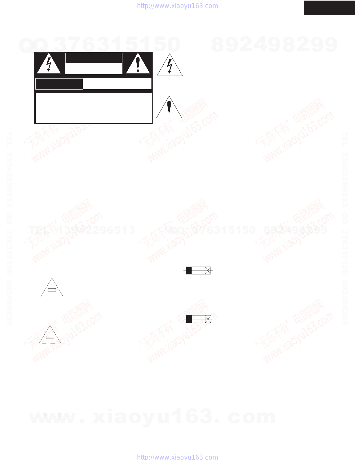
SAFETY-RELATED COMPONENT
WARNING!!
COMPONENTS IDENTIFIED BY MARK ON THE
SCHEMATIC DIAGRAM AND IN THE PARTS LIST ARE
CRITICAL FOR RISK OF FIRE AND ELECTRIC SHOCK.
REPLACE THESE COMPONENTS WITH ONKYO
PARTS WHOSE PART NUMBERS APPEAR AS SHOWN
IN THIS MANUAL.
MAKE LEAKAGE-CURRENT OR RESISTANCE
MEASUREMENTS TO DETERMINE THAT EXPOSED
PARTS ARE ACCEPTABLY INSULATED FROM THE
SUPPLY CIRCUIT BEFORE RETURNING THE
APPLIANCE TO THE CUSTOMER.
STANDBY / ON
STANDBY
SETUP
PHONES
AUDIO NETWORK RECEIVER
Silver model only
120V AC, 60HzTUDD
Q
3
Q
Restoring the factory default settings:
To reset all the stored settings to the factory
default conditions, while the power to the NC-500
is on, press and hold down the STOP button on
the unit, and press STANDBY/ON button.
7
6
AUDIO
INPUT
DISPLAY
SELECT
3
1
VOLUME
5
TEL 13942296513 QQ 376315150 892498299
-
NC
500
9
9
2
8
9
4
2
9
8
0
5
1
w
w
w
.
xia
o
y
u
1
6
3
.
c
o
m
Page 2

Specifications
NC-500
Amplifier Section
Q
Q
Power output
FTC 15 watts per channel, min RMS, at 8 ohms,
both channels driven 1 kHz, with no more
than 0.1%
DIN 2 × 17 watts at 6 Ω, 1 kHz
2 × 15 watts at 8 Ω, 1 kHz
Dynamic power output
2 × 27 watts at 6 Ω
2 × 24 watts at 8 Ω
Total harmonic distortion
0.1% at rated power
TEL 13942296513 QQ 376315150 892498299
IM distortion
0.6% at rated power
Damping factor
30 at 8 Ω
Input Sensitivity and Impedance
TAPE/MD PLAY: 150 mV, 50 kΩ
LINE IN: 150 mV, 50 kΩ
Frequency and response
10 to 50,000 Hz +0 /–3 dB
Signal to noise ratio
100 dB (IHF-A)
Muting
–60 dB
TEL
3
7
6
3
1
13942296513
Tuner Section
5
1
5
Tuning range
FM: 87.50–108.00 MHz (100 kHz steps)
AM: 530–1710 kHz (10 kHz steps)
Usable sensitivity
FM: Mono 11.2 dBf,
AM: 30 µV
50 dB Quieting sensitivity
FM: Mono 17.2 dBf, 2.0 µV (75 Ω)
Capture ratio
FM: 2.0 dB
Image rejection ratio
FM: 40 dB (U.S. & Canadian models)
AM: 40 dB
IF rejection ratio
FM: 90 dB
AM: 40 dB
Signal to noise ratio
FM: Mono 73 dB, IHF
AM: 40 dB
Selectivity
FM: 50 dB DIN
AM Suppression Ratio
50 dB
Harmonic distortion
FM: Mono 0.2%
AM: 0.7 %
Frequency response
FM: 30–15,000 Hz (±1.5 dB)
Stereo separation
FM: 45 dB at 1,000 Hz
Stereo threshold
FM: 17.2 dBf, 2.0 µV (75 Ω)
0
(U.S. & Canadian models)
87.5–108.00 MHz (50 kHz steps)
(Other area models)
(U.S. & Canadian models)
522–1611 kHz (9 kHz steps)
(Other area models)
1.0 µV (75 Ω IHF)
0.9 µV (75 Ω DIN)
Stereo 17.2 dBf,
2.0 µV (75 Ω IHF)
23.0 µV (75 Ω DIN)
Stereo 37.2 dBf, 20.0 µV (75 Ω)
85 dB (Other area models)
3
Q
Q
Stereo 67 dB, IHF
(±300 kHz at 40 kHz Devi.)
Stereo 0.3%
30 dB at 100 to 10,000 Hz
7
8
6
3
1
9
5
2
1
5
0
4
9
8
9
2
8
4
2
9
8
2
9
9
9
TEL 13942296513 QQ 376315150 892498299
9
w
w
w
.
xia
o
y
u
1
6
3
.
c
o
m
Page 3
WARNING
AVIS
OPERATING INSTRUCTIONS
NC-500
SAFETY PRECAUTIONS
Q
Q
WARNING : TO REDUCE THE RISK. OF
ELECTRIC SHOCK, DO NOT REMOVE
COVER(OR BACK). NO USERSERVICEABLE
PART INSIDE, REFER SERVICING TO
QUALIFIED SERVICE PERSONNEL.
TEL 13942296513 QQ 376315150 892498299
TO REDUCE THE RISK OF FIRE OR ELECTRIC SHOCK, DO NOT EXPOSE THIS APPLIANCE TO RAIN
WARNING :
OR MOISTURE. DANGEROUS HIGH VOLTAGES ARE PRESENT INSIDE THE ENCLOSURE. DO NOT OPEN THE
CABINET. REFER SERVICING TO QUALIFIED PERSONNEL ONLY.
CAUTION :
TO PREVENT ELECTRIC SHOCK, MATCH WIDE BLADE OF PLUG TO WIDE SLOT, FULLY INSERT.
POUR EVITER LES CHOCS ELECTRIQUE, INTRODUIRE LA LAME LA PLUS LARGE DA LA FICHE DANS LA
ATTENTION :
BORNE CORRESPONDANTE DA LA PRISE ET POUSSER JUSQU' AU FOND.
PRECAUTIONS
7
3
AVIS
6
WARNING
RISK OF ELECTRIV SHOCK
DO NOT OPEN
RISQUE DE CHOC ELECTRIQUE NE
3
1
5
P AS OUVRIR
1
5
0
The lightning flash with arrowhead symbol, within an equilateral triangle, is
intended to alert the user to the presence of uninsulated "dangerous voltage"
within the product's enclosure that may be of sufficient magnitude to constitute
a risk of electric shock to persons.
The exclamation point within an equilateral triangle is intended to alert the user
to the presence of important operating and maintenance (servicing) instruction
in the literature accompanying the appliance.
8
9
2
4
9
8
2
9
9
TEL 13942296513 QQ 376315150 892498299
1. Replacing the fuses
TEL
2. Safety-check out (Only U.S.A. model)
w
13942296513
For continued protection against risk fire, replace only with same type and same rating fuse.
CIRCUIT No. PART No. DESCRIPTION
F911 <UD> 252166 6.3A-UL/T-237
CAUTION
FOR CONTINUED PROTECTION
AGAINST FIRE HAZARD, REPLACE
ONLY WITH FUSE OF SAME TYPE
VA
AND RATING INDICATED.
ATTENTION
AFIN D'ASSURER UNE PROTECTION
PERMANENTE CONTRE LES RISQUES
D'INCENDIE, REMPLACER UNIQUEMENT
VA
PAR UN FUSIBLE DE MEME TYPE
ET CALIBRATION COMME INDIQUE.
After correcting the original service problem, perform the following safety check before releasing the set
to the customer. Connect the insulating-resistance tester between the plug of power supply cord and screw
on the back panel.
Specifications: 3.3Mohm+/-10% at 500V.
w
w
.
xia
o
y
u
Q
1
Q
7
3
THIS SYMBOL LOCATED NEAR THE FUSE INDICATES
THAT THE FUSE USED IS SLOW OPERATING TYPE
FOR CONTINUED PROTECTION AGAINST FIRE
HAZARD,REPLACE WITH SAME TYPE FUSE. FOR FUSE
RATING REFER TO THE MARKING ADJACENT TO THE SYMBOL
CE SYMBOLE INDIQUE QUE LE FUSIBLE UTLISE EST
E LENT. POUR UNE PROTECTION PERMANENTE,N'UTILISER
QUE DES FUSIBLES DE MEME TYPE. CE DARNIER EST
INDIQUE LA QU LE PRESENT SYMBOL EST APPOSE.
6
3
6
3
.
1
1
5
c
5
o
0
m
8
9
2
4
9
8
2
9
9
Page 4
NC-500
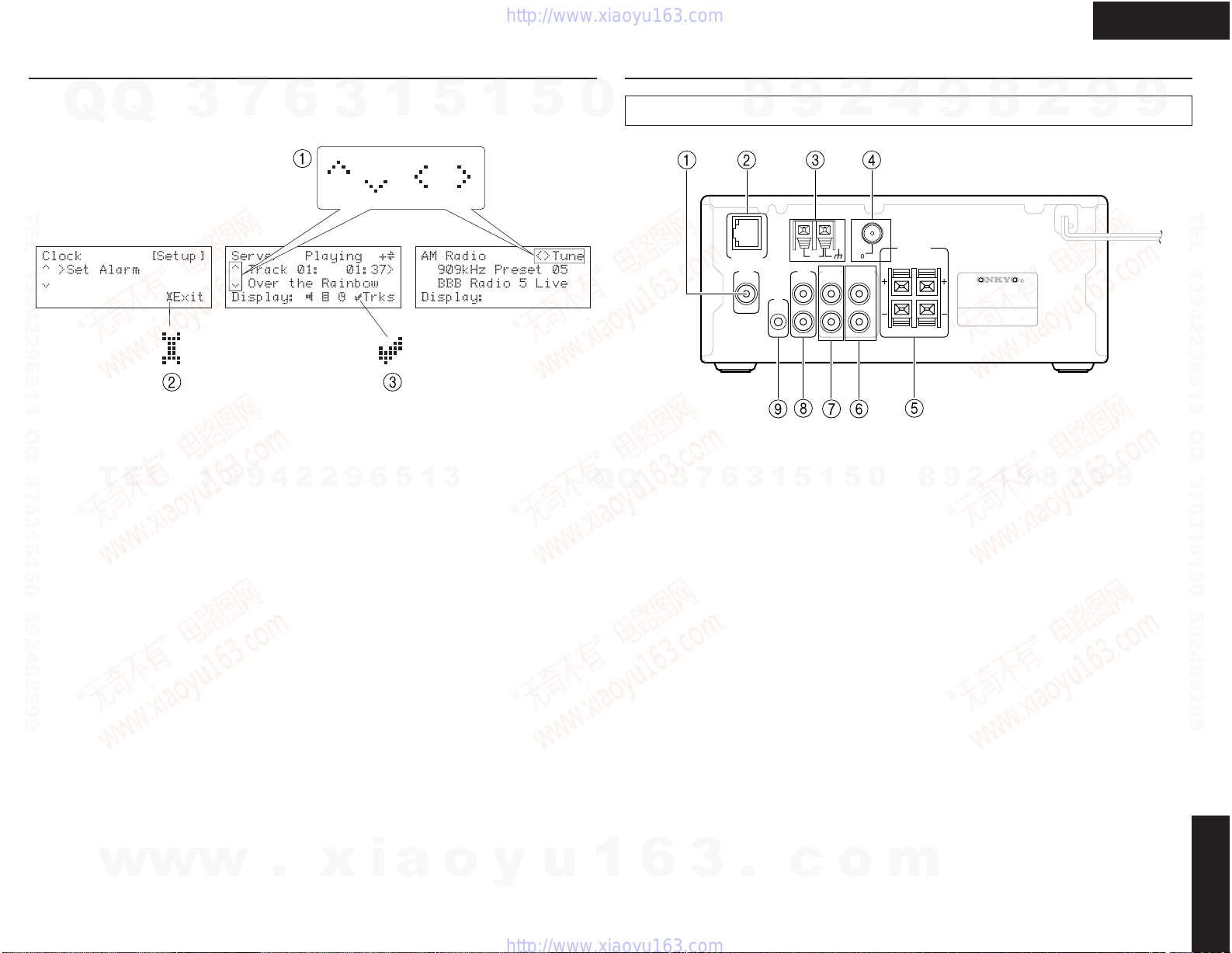
Index parts and facilities
Remote Controller
Q
TEL 13942296513 QQ 376315150 892498299
Q
3
TEL
7
6
13942
3
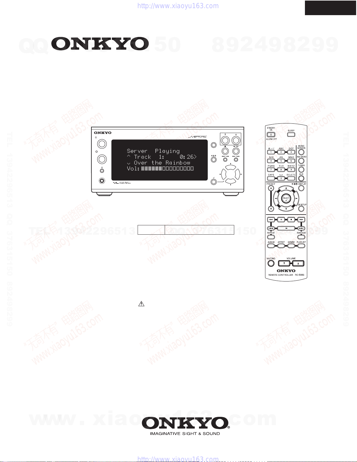
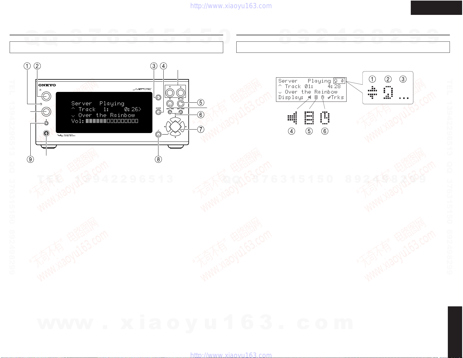
1 STANDBY/ON button
2 Numeric keys
3 PRESET Up/Down buttons
4 ALBUM button
5 ARTIST button
296
1
Turns on the NC-500 or place it in standby
mode. When the NC-500 is in standby mode,
you can use this button to turn off the alarm.
Press to select one of the preset stations or the
track you want to play. When entering text,
you use these buttons to type in letters and
special characters.
Press to navigate through preset stations for
Internet radio or FM/AM radio.
Press to invoke the Album selection menu
when working with the Net-Tune Central.
Press to invoke the Artist selection menu
when working with the Net-Tune Central.
5
513
1
5
0
Q
Index parts and facilities
B Cursor / / / buttons
Press to locate your selection.
C SELECT button
Press to save a new setting.
D SETUP button
Press to set up the NC-500.
E Operation buttons
, (FR/FF) buttons
Press to fast-rewind or fast-forward the
current track.
(Pause) button
Press to pause the playback.
(Play) button
Press to start playback.
(Stop) button
Press to stop the playback.
, B/F-Skip buttons
Press to move to the previous or next track.
F RANDOM button
Q
3
Press to play the selected track list at random.
7
8
6
3
1
9
5
1
2
5
0
4
Changing the remote controller
9
mode
When you use any Onkyo products other than the
NC-500 in the same room, the operations made
with the NC-500's remote controller may also
cause the other Onkyo products to operate. To
avoid this, you can change the remote controller
mode both for the NC-500 and its remote
controller choosing from three modes (1, 2 or 3).
To change the remote controller mode for the
remote controller, hold the STANDBY button on
the remote controller and press the SELECT
button, then release these buttons simultaneously.
Within 5 seconds after releasing the buttons, enter
the appropriate mode (1, 2 or 3) using the numeric
keys. The default mode is 1 for both the remote
controller and NC-500.
After changing the remote controller mode, make
sure that the remote control code on the NC-500 is
set to the same mode as the remote controller. (see
Page 63)
8
9
8
2
4
9
2
8
2
9
9
9
TEL 13942296513 QQ 376315150 892498299
9
w
w
w
.
6 GENRE button
Press to invoke the Genre selection menu
when working with the Net-Tune Central.
7 PLAYLIST button
Press to invoke the Playlist selection menu
when working with the Net-Tune Central.
8 MUTING button
Press to activate the mute function. Press the
button again to disable the mute function.
9 SLEEP button
Press to set the sleep function.
0 MUSIC SERVER/iNetRADIO/TUNER/
AUX buttons
Press to select an input source. The TUNER
button toggles between FM and AM.
A DISPLAY button
x
i
Press to change the display mode.
a
o
y
u
G REPEAT button
Press to repeat the selected single track or
track list.
H VOLUME / buttons
Press to adjust the volume.
1
6
3
.
c
o
NC-500
m
Page 5
NC-500
Index parts and facilities
(2) Operation guide icons
Q
TEL 13942296513 QQ 376315150 892498299
1 Up Arrow/ /Down Arrow/Left Arrow/Right Arrow
These icons are displayed to indicate that the corresponding cursor buttons are enabled to perform
specific actions.
Example: “< >
when the FM/AM radio feature is selected.
2 Setup
This icon is immediately followed by the command you can execute by pressing the SETUP button.
Example: When the Setup icon is immediately followed by “EXIT”, you can press the SETUP
button to exit from the current menu.
3 Select
This icon is immediately followed by the command you can execute by pressing the SELECT
button.
Q
TEL
Tune” indicates that you can use the Cursor Left and Right buttons to perform tuning
3
7
6
13942
3
296
1
513
5
1
5
Index parts and facilities
0
Rear Panel
1 OSD OUT
Q
Q
2 ETHERNET
3 AM
7
3
This port can be used to redirect screen output
from the front panel display to a television
screen for quick and easy large-screen
viewing.
This port connects to a broadband mode,
router, hub, etc.
This port connects to the AM radio antenna.
UDD
6
8
27123044
ETHERNET
OSD
3
IR
IN
1
9
AM
AUX
FIXED VARIABLE
INOUT OUT OUT
L
R
1
5
2
ANTENNA
FM
75
5
L
R
0
4
SPEAKERS
(
6 OHMS MIN.
R
4
2
NC-
500
9
9
)
L
8 AUX
8
9 IR IN
8
AUDIO NETWORK RECEIVER
MODEL NO.
2
9
This port connects to an auxiliary device.
If the NC-500 is located inside a rack or a
cabinet that will not allow infrared beams to
reach its IR sensor, you will need to relay
beams with an external sensor.
Connect the external sensor to IR IN input.
Then, place the sensor in an unblocked
location at which you can easily point with
the remote controller.
8
9
2
9
9
9
TEL 13942296513 QQ 376315150 892498299
w
w
w
.
x
i
a
o
4 FM
This port connects to the FM radio antenna.
5 SPEAKERS
The terminals connect to the speakers.
6 VARIABLE OUTPUT
This port connects to an amplifier without
volume control.
7 FIXED OUT
y
u
1
This port connects to the input port of a
6
receiver with volume control.
3
.
c
o
NC-500
m
Page 6
NC-500
Index parts and facilities
Q
Front Panel
TEL 13942296513 QQ 376315150 892498299
Remote
control
sensor
1 STANDBY indicator
Lights when the NC-500 is in the Standby
mode.
2 STANDBY/ON button
Switches the power mode between Standby
and On.
3 AUDIO INPUT button
Changes the playback source.
4 DISPLAY button
Changes the screen content.
5 Play/Pause button
Starts or pauses playback.
Q
STANDBY / ON
STANDBY
SETUP
PHONES
PHONES
jack
TEL
3
AUDIO NETWORK RECEIVER
7
6
13942
3
296
8 SELECT button
9 SETUP button
1
AUDIO
INPUT
DISPLAY
SELECT
5
Master
volume
VOLUME
-
NC
1
500
513
Saves a new setting.
Activates Setup/Menu mode.
5
Stop
0
Q
Index parts and facilities
3
9
1
Display
8
(1) Status display icons
1 Random
This icon is displayed to indicate that the NC-500 is in random playback mode.
2 Repeat
6
7
Q
3
This icon is displayed to indicate that the NC-500 is in repeat mode.
3 Ellipsis
Indicates that the text continues.
4 Status
This icon is enclosed in square brackets to indicate that the NC-500 is in normal mode.
5 Browse
This icon is enclosed in square brackets to indicate that the NC-500 is in browse (title selection)
mode.
6 Clock
This icon is enclosed in square brackets to indicate that the NC-500 is in clock display mode.
5
2
1
5
0
4
8
9
9
8
2
4
9
2
8
2
9
9
9
TEL 13942296513 QQ 376315150 892498299
9
6 F/B-Skip buttons
Moves to the previous or next track. Holding
down the either button fast-forwards or fastrewinds the current track.
7 Cursor Up/Down/Right/Left buttons
Use these buttons when navigating through
various settings, change a value, or move to
another menu.
w
w
w
.
x
i
a
o
y
u
1
6
3
.
c
o
NC-500
m
Page 7
NC-500
Q
TEL 13942296513 QQ 376315150 892498299
Q
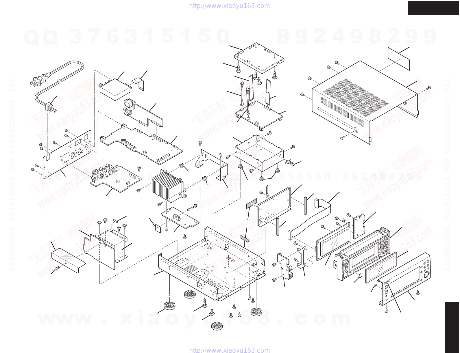
EXPLODED VIEW
TEL
A060
3
A105
A101
7
13942296513
U004
U002
6
3
U101D
F901
A120
T901
1
P101
U003
Q501A
5
U000
1
U001
5
A016
A017
A016
0
A026
P609
P602
P606
A025
Q
A015
Q
A016
A013
3
7
6
A016
8
P601
3
A013
U009
1
9
A029
5
A040
1
2
5
A013
0
4
P7001
8
9
9
2
8
4
U006
9
2
8
A110
2
9
A315
A310
9
A112
9
TEL 13942296513 QQ 376315150 892498299
9
A061
w
w
w
.
x
A008
i
A009
a
o
A055
y
u
A017
1
6
3
U005
.
A113
c
Q7005
o
A111
A302
A301
NC-500
A305
m
Page 8
r
NC-500
A
BCD
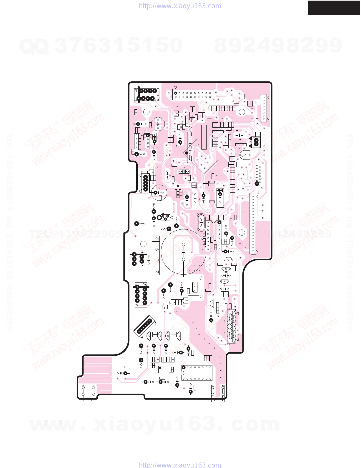
SCHEMATIC DIAGRAMS
Network Circuit Section - 1/2
7
P606B
1
2
3
4
5
BM05B-SRSS-TB
R661
3
C601
C693
100/6.3
0
47/6.3
+
Q
1
Q
TEL 13942296513 QQ 376315150 892498299
P602B
2
3
TEL
4
5
w
1
2
3
4
B4B-PH-SM3-TB
To VLC Board
C644
AGND
D/A Convertor
13942296513
+3.3V
VAL
VAL
C670
C671
+5.6V
5
4
3
2
1
B5B-PH-SM3-TB
P607B
E601
C672
NC
1
2
3
C674
NC
4
Terminal
E602
C675
NC
1
2
3
C676
NC
4
Terminal
E603
C677
NC
1
2
3
C680
NC
4
Terminal
E604
C681
NC
1
2
3
C697
NC
4
Terminal
+3.3V
Reset IC
Q615
5
VAL
C691
1
w
w
6
3.3V 2.5V Voltage Regurator
L603
R696
+
OUT
C632
C635
NC
NC
NC
D605
1SS352
VAL
2
BYPASS
GND
R608
0
R610
0
AVDD = +5V
100/6.3
+
C639
C638
AVDD = +5V
+
C648
C647
100/6.3
R697
4
3
.
+5.6V
47/16Ta
C614
4
VO
3
+
10/16
C694
0.1
+
C640
C641
220/4
+
0.1
C649
220/4
NC
R631
NC
R632
NC
R633
BICK
LRCK
SDTI
MCKI
MCKO
SCL
SDA
CSN
PDN
TX
NC
TST
TTL
I2C
5
1
2
3
4
6
7
8
VAL
9
10
+3.3V
VAL
R560
R680
+
0.1
6
8
7
5
1
11
12
10
9
2
23
13
14
15
VAL
xia
+5.6V
NFM60R10T471
VAL
R695
Q617 NJM2370U05
5
VIN
1
CONT
+
0.1
C645
100/6.3
A
D604
1SS352
C696
0.001
Q611
18
OUTR
19
OUTL
16
CAD0
17
CAD1
3
DVDD
22
AVDD
20
VCOM
21
AVSS
4
DVSS
24
DZF
VAL
Audio DIT
A
VDD
CD
VSS
VAL
2
3
1
2
C692
0.1
Q605
21
ZERO
16
VOUTL
13
VOUTR
15
AVDD
9
AVDDR
11
VMIDR
10
AGNDR
20
AVDDL
18
VMIDL
0.1
C650
19
AGNDL
14
AGND
+3.3V
OPTSIGNAL
1
5
1
5
0
Q607
83
COL7
84
COL6
85
COL5
86
COL4
87
COL3
88
COL2
91
COL1
92
COL0
23
PA7
24
PA6
25
PA5
26
PA4
27
PA3
28
PA2
62
PD0/LEDFLSH
45
PE2/CLKSEL
46
PE1/BOOTSEL1
47
PE0/BOOTSEL0
56
PD4
155
MEDCHG/BROM
39
TEST1
40
TEST0
75
DRIVE1
76
DRIVE0
67
SSIRXDA
63
SSICLK
65
SSITXFR
66
SSITXDA
93
BUZ
68
SSIRXFR
13
PB7
14
PB6
15
PB5
16
PB4
17
PB3
18
PB2
19
PB1/PRDY2
20
PB0/PRDY1
188
DD3
189
DD2
191
DD1
192
DD0
34
PHDIN
157
VddOSC
Q
160
VssOSC
184
CL2
185
CL1
186
FRM
187
M
31
LEDDRV
79
SMPCLK
161
WAKEUP
55
PD5
7
RUN/CLKEN
5
WORD
105
HALFWORD
70
ADCCS
77
ADCCLK
78
ADCOUT
181
VddCORE1
72
VddCORE0
0.1
180
VssCORE1
71
VssCORE0
59
PD3
37
DCD
38
DSR
35
CTS
36
RXD1
61
PD1
60
PD2
32
TXD1
154
POR
69
ADCIN
156
URESET
125
TRST
11
TDI
58
TMS
90
TXCLK
22
TDO
+3.3V
197
VddIO10
NC
52
6
MultiMedia CPU
123
139
167
183
VddIO7
VddIO8
VddIO9
3
VssIO17
VssIO16
VssIO15
203
198
190
182
XTRST
TDI
TMS
TXCLK
TDO
3
XURESET
+3.3V+2.5V
BA33C25FP
Q601
VIN
NC
2
XDITCS
XDITCS
VAL
R671
XDITCS
XDITPD
XDITPD
4.7K
R672
XDITPD
GND
3
CSBIWO
MODE8X
WM8716
RSTB
MCDM127MDMD026MLI2S28MUTEB
22
0
R6360R637
R635
XDARST
DIGCL
DIGDO
XDARST
DIGCL
DIGDO
VAL
VAL
4.7K
R673
R674
R675
XDARST
DIGCL
DIGDO
VO1
VO2
C613
C627
CLKO
DIFFHW
MODE
DVDD
DGND
BCKIN
LRCIN
0
XDACS
XDACS
VAL
R676
XDACS
0.1
0.1
XTO
DIN
XTI
25
2
VAL
R638
DAMUTE
DAMUTE
VAL
R677
DAMUTE
4
L601
BLM21P221SG
5
+
4.7/10Ta
C602
23
4
17
12
24
NC
L607
47uH
R616
8
0.1
C636
7
3
1
2
5
6
R559
VAL
R650
47K
1 7
0.1
C663
R670
R681
VAL
o
+3.3V
0.1
C603
+
+3.3V
100/6.3Ta
C615
0.1
C616
+3.3V
R648
10K
+3.3V
10K
R611
+
C637
100/6.3Ta
NC
+3.3V
R626
NC
0.1
C651
X601
10K
10K
10K
R644
R645
R643
WakeUP
+3.3V
0.1
C658
1
Q609A
2
TC7W14FK
10K
R651
+3.3V
10K
R557
10K
10K
R552
R551
XRESET
+3.3V +3.3V
10K
R669
XURESET
0.1
C684
VAL
Q609B
TC7W14FK
3 5
y
10K
R612
R621NCR620
4
FCXO-03
1
10K
R646
10K
R550
0.1
C604
0.1
C617
0.1
C605
C606
0.1
C618
C619
+3.3V
+3.3V
10K
R609
10K
10K
R613
R614
JP1
JP2
JP3
NC
R622
TP601
BCLK
LRCK
SDATA
R625
256fs
11.2896MHz
2 3
10K
R647
+3.3V
5
4
VCC
G
3
Q610
TC7S02F
COM1_DCD
COM1_DSR
COM1_CTS
COM1_RXD1
COM1_TXD1
u
0.1
0.1
R667
C607
R606
R615
+3.3V
10K
R623
0
+2.5V
0.1
C652
Q
0.1
C659
10K
C620
0.1
0.1
330
D603
SEC1201C
10K
+2.5V
C673
1
107
VddIO6
7
VssIO14
174
VssIO13
168
4
2
9
8
+2.5V
0.1
C608
48
51
VddIO02VddIO121VddIO257VddIO374VddIO489VddIO5
VssRTC
VddRTC
EP7312-CV
1
3
6
VssIO581VssIO473VssIO364VssIO233VssIO112VssIO0
VssIO12
VssIO11
VssIO10
VssIO9
VssIO8
VssIO7
VssIO6
98
149
140
124
116
108
LANRESET
DAMUTE
XDACS
DIGDO
DIGCL
XDARST
XDITPD
XDITCS
(XURESET)
(XPOR)
XRESET
OPTSIGNAL OPTSIGNAL
.
c
5
WRITE/SDRAS
1
SDCS1
SDCS0
MOE/SDCAS
MWE/SDWE
SDCLK
SDCKE
SDQM3
SDQM2
PD7/SDQM1
PD6/SDQM0
EXPCLK
EXTPWR
EINT3
EINT2
EINT1
EINT0
PWRFL
BATOK
BATCHG
RTCOUT
RTCIN
EXPRDY
MOSCOUT
MOSCIN
3
A27
A26
A25
A24
A23
A22
A21
A20
A19
A18
A17
A16
A15
A14
A13
A12
A11
A10
A9
A8
A7
A6
A5
A4
A3
A2
A1
A0
D31
D30
D29
D28
S27
D26
D25
D24
D23
D22
D21
D20
D19
D18
D17
D16
D15
D14
D13
D12
D11
D10
D9
D8
D7
D6
D5
D4
D3
D2
5
D1
D0
CS5
CS4
CS3
CS2
CS1
CS0
PA1
PA0
FB1
FB0
TXD2
RXD2
o
99
101
103
106
110
112
114
117
119
121
126
128
130
132
134
136
138
142
144
146
148
163
165
169
171
173
176
178
94
95
96
97
100
102
104
109
111
113
115
118
120
122
127
129
131
133
135
137
141
143
145
147
150
164
166
170
172
175
0
177
179
193
194
6
202
201
200
199
195
196
53
54
4
1
208
207
206
205
204
152
41
42
43
44
162
153
151
49
50
29
30
80
82
8
9
10
159
158
A27
A26
A25
A24
A23
A22
A21
A20
A19
A18
A17
A16
A15
A14
A13
A12
A11
A10
A9
A8
A7
A6
A5
A4
A3
A2
A1
A0
D31
D30
D29
D28
D27
D26
D25
D24
D23
D22
D21
D20
D19
D18
D17
D16
D15
D14
D13
D12
D11
D10
D9
D8
D7
D6
D5
D4
D3
D2
D1
D0
XSDRAMCS
XSDRAS
XOE
XWE
SDCLK
SDCKE
SDQM3
SDQM2
SDQM1
SDQM0
XLANCS
XFLASHCS
XEXTPWR
LANINT
XEXTIRQ2
XISAINT
XEXTFIQ
XPWRFL
BATOK
XBATCHG
10K
R687
32K
I2C_CLK
I2C_DATA
+3.3V
C682
EXPRDY
COM2_TXD
COM2_RXD
R682
100
X604
15P
C685
m
8
R688
VAL
3.6864MHz
10K
X603
VAL
9
+3.3V
C621
+3.3V
0.1
C630
C629
XSDRAMCS
XOE
XSDRAS
9
10K
10K
R689
R690
VAL
C683
+3.3V
15P
C686
0.1
C687
0.1
0.1
XWE
2
R691
C688
10K
0.1
8
0.1
0.1
C623
C622
0.1
C631
SDQM3
SDCKE
SDCLK
4
EXTPWR
LANINT
10K
R692
0.1
C689
XTRST
TDI
TMS
TXCLK
TDO
XURESET
SDQM2
1K
+3.3V
C624
0.1
9
R656
2
R658
C666
C690
2
A13
A14
A15
A16
A17
A18
A19
A20
A21
A22
A23
A24
A25
A26
A27
XSDRAMCS
XSDRAS
XOE
XWE
SDCLK
SDCKE
SDQM3
SDQM2
A13
A14
A15
A16
A17
A18
A19
A20
A21
A22
A23
A24
A25
A26
A27
XSDRAMCS
XSDRAS
8
XOE
XWE
SDCLK
SDCKE
SDQM3
SDQM2
2
+3.3V +3.3V
+3.3V
VAL
R659
0.1
0.1
R603
R604
+3.3V
0.1
C643
R628
R629
2
+3.3V
1K
R655
10K
0.1
C667
C668
LANRESET
DAMUTE
XDACS
DIGDO
DIGCL
XDARST
XDITPD
XDITCS
(XURESET)
(XPOR)
XRESET
9
Main Memo
Q603
21
BS1
20
BS0
0
36
A12/NC
0
35
A11
22
A10
34
A9
33
A8
32
A7
31
A6
30
A5
29
A4
26
A3
25
A2
24
A1
23
A0
19
CS
18
RAS
17
CAS
16
WE
38
CLK
37
CKE
39
UDQM
15
LDQM
27
Vcc2
14
Vcc1
1
Vcc0
54
Vss2
41
Vss1
28
Vss0
Q608
21
BS1
20
BS0
0
36
A12/NC
0
35
A11
22
A10
34
A9
33
A8
32
A7
31
A6
30
A5
29
A4
26
A3
25
A2
24
A1
23
A0
19
CS
18
RAS
9
9
17
CAS
16
WE
38
CLK
37
CKE
39
UDQM
15
LDQM
27
Vcc2
14
Vcc1
1
Vcc0
0.1
C665
54
Vss2
41
Vss1
28
Vss0
10K
R660
+3.3V
+3.3V
10K
R662
0.1
0.1
C669
9
DQ15
DQ14
DQ13
DQ12
DQ11
DQ10
DQ9
DQ8
DQ7
DQ6
DQ5
DQ4
DQ3
DQ2
DQ1
DQ0
HM5264165FTT-B6
NC
VccQ3
VccQ2
VccQ1
VccQ0
VssQ3
VssQ2
VssQ1
VssQ0
DQ15
DQ14
DQ13
DQ12
DQ11
DQ10
DQ9
DQ8
DQ7
DQ6
DQ5
DQ4
DQ3
DQ2
DQ1
DQ0
HM5264165FTT-B6
NC
VccQ3
VccQ2
VccQ1
VccQ0
VssQ3
VssQ2
VssQ1
VssQ0
COM2_TXD
COM2_RXD
LANRESET
53
51
50
48
47
45
44
42
13
11
10
8
7
5
4
2
TEL 13942296513 QQ 376315150 892498299
40
49
43
9
3
52
46
12
6
53
51
50
48
47
45
44
42
13
11
10
8
7
5
4
2
0.1
C653
40
49
43
9
3
52
46
12
6
DIGDO
XDACS
DAMUTE
Page 9
T
C624
R656
NC-500
A
BCD
SCHEMATIC DIAGRAMS
Network Circuit Section - 2/2
Q
Q
3
6
7
1
Main Memory Program Flash ROM
A13
A14
A15
A16
0.1
A17
A18
A19
A20
A21
A22
A23
A24
A25
TEL 13942296513 QQ 376315150 892498299
A26
A27
XSDRAMCS
XSDRAS
XOE
XWE
SDCLK
SDCKE
SDQM3
SDQM2
2
A13
A14
A15
A16
A17
A18
A19
A20
A21
A22
A23
A24
A25
A26
A27
XSDRAMCS
XSDRAS
3
TEL
XOE
XWE
SDCLK
SDCKE
SDQM3
SDQM2
WR
T
2
2
.3V
+3.3V
4
VAL
R658
0.1
C666
0.1
C690
5
w
Q603
21
BS1
20
BS0
0
36
R603
A12/NC
0
35
R604
A11
22
A10
34
A9
33
A8
32
A7
31
A6
30
A5
29
A4
26
A3
25
A2
24
A1
23
A0
19
CS
18
HM5264165FTT-B6
RAS
17
CAS
16
WE
38
CLK
37
CKE
39
UDQM
15
LDQM
+3.3V
27
Vcc2
14
Vcc1
1
Vcc0
0.1
C643
54
Vss2
41
Vss1
28
Vss0
Q608
21
BS1
20
BS0
0
36
R628
A12/NC
0
35
R629
A11
22
A10
34
A9
33
A8
32
A7
31
A6
30
A5
29
A4
26
A3
25
A2
24
A1
23
A0
19
CS
18
HM5264165FTT-B6
RAS
13942296513
17
CAS
16
WE
38
CLK
37
CKE
39
UDQM
15
LDQM
+3.3V
27
Vcc2
14
Vcc1
1
Vcc0
0.1
C665
54
Vss2
41
Vss1
28
Vss0
1K
R655
10K
R660
10K
R659
+3.3V
+3.3V
0.1
0.1
C667
C668
LANRESET
DAMUTE
XDACS
DIGDO
DIGCL
XDARST
XDITPD
XDITCS
(XURESET)
(XPOR)
XRESET
OPTSIGNAL
w
10K
R662
0.1
C669
w
COM2_TXD
DQ15
DQ14
DQ13
DQ12
DQ11
DQ10
DQ9
DQ8
DQ7
DQ6
DQ5
DQ4
DQ3
DQ2
DQ1
DQ0
NC
VccQ3
VccQ2
VccQ1
VccQ0
VssQ3
VssQ2
VssQ1
VssQ0
DQ15
DQ14
DQ13
DQ12
DQ11
DQ10
DQ9
DQ8
DQ7
DQ6
DQ5
DQ4
DQ3
DQ2
DQ1
DQ0
NC
VccQ3
VccQ2
VccQ1
VccQ0
VssQ3
VssQ2
VssQ1
VssQ0
COM2_RXD
LANRESET
DAMUTE
D31
53
D30
51
D29
50
D28
48
D27
47
D26
45
D25
44
D24
42
D23
13
D22
11
D21
10
D20
8
D19
7
D18
5
D17
4
D16
2
40
49
43
9
3
0.1
C642
52
46
12
6
D15
53
D14
51
D13
50
D12
48
D11
47
D10
45
D9
44
D8
42
D7
13
D6
11
D5
10
D4
8
D3
7
D2
5
D1
4
D0
2
0.1
C653
0.1
C654
40
+3.3V
49
43
9
3
0.1
C664
52
46
12
6
XWE
XOE
XLANCS
XFLASHCS
XDITCS
XDITPD
XDARST
DIGCL
DIGDO
XDACS
.
xia
3
0.1
C655
XWE
XOE
LANRESET
XRESET
(XPOR)
(XURESET)
A21
A20
A19
A18
A17
A16
A15
A14
A13
A12
A11
A10
A9
A8
A7
A6
A5
A4
A3
A2
A1
XWE
XOE
XFLASHCS
XLANINT
XFLASHCS
XLANCS
OPTSIGNAL
XTRST
1
10
9
16
17
48
1
2
3
4
5
6
7
8
18
19
20
21
22
23
24
25
11
28
26
EXPRDY
TDI
TMS
TXCLK
TDO
Q604
A20
A19
A18
A17
A16
A15
A14
A13
A12
A11
A10
A9
A8
A7
A6
A5
A4
A3
A2
A1
A0
WE
OE
CE
XRESET
XURESET
5
0.1
C625
37
VCC
MX29LV320BTC-90
BYTE
RY/BY
WP/ACC
RESET
VSS2
VSS1
27
46
OPTSIGNAL
o
+3.3V
D15
D14
D13
D12
D11
D10
D9
D8
D7
D6
D5
D4
D3
D2
D1
D0
NC
1
0.1
C626
D15
45
D14
43
D13
41
D12
39
D11
36
D10
34
D9
32
D8
30
D7
44
D6
42
D5
40
D4
38
D3
35
D2
33
D1
31
D0
29
+3.3V +3.3V+3.3V
13
10K
R617
47
15
14
12
y
5
10K
R618
XRESET
C670
C671
C682 NC
C683 NC
C684 0.1
C691 0.1
P601
P603A
P604B
P606B
P608B
P610B
R559
R560
R561
R619
R624
R638
R639
R640
R641 NC
D15
D14
D13
D12
D11
D10
D9
D8
D7
D6
D5
D4
D3
D2
D1
D0
+3.3V
10K
R627
XWE
XOE
XLANCS
LANINT
EXPRDY
LANRESET
+3.3V
10K
R558
1 7
COM2_TXD
COM2_RXD
DAMUTE
XDACS
DIGDO
DIGCL
XDARST
XDITPD
XDITCS
(XURESET)
(XPOR)
NC-500
NC
NC
NC
NC
NC
BM05-SRSS-TB
52610-1390
52610-1390
NC
10K
NC
NC
NC
0
NC
NC
u
0
+3.3V
A3
A2
A1
+3.3V+3.3V
Q
10K
R649
+3.3V
L605
BLM21P221SG
L606
BLM21P221SG
Q618A
TC7W14FK
COM2_TXD
1
60
59
58
54
53
52
51
50
48
47
46
45
44
43
42
41
40
39
38
37
18
19
20
21
24
25
26
27
74
73
72
71
68
67
66
65
7
2
28
29
62
61
49
36
63
34
33
32
64
35
30
31
75
11
12
Q
13
14
15
16
6 2
COM2_RXD
R658 10K
R670
R671
R674
R675
R676
R677
R680
R681
R695 NC
R696 NC
R697
Q611
Q615
X603
Q616
SA19
SA18
SA17
SA16
SA15
SA14
SA13
SA12
SA11
SA10
SA9
SA8
SA7
SA6
SA5
SA4
SA3
SA2
SA1
SA0
SD15
SD14
SD13
SD12
SD11
SD10
SD9
SD8
SD7
SD6
SD5
SD4
SD3
SD2
SD1
SD0
CHIPSEL
ELCS
MEMW
MEMR
IOW
IOR
REFRESH
SBHE
AEN
MEMCS16
IOCS16
INTRQ0
IOCHRDY
INTRQ3
INTRQ2
INTRQ1
RESET
DMARQ2
DMACK2
DMARQ1
DMACK1
DMARQ0
DMACK0
Q618C
6
9
3
95
0.1
0.1
C662
C661
C660
TC7W14FK
Q609C
TC7W14FK
6 2
10K
R657
XTRST
TDI
TMS
TXCLK
TDO
XURESET
NC-500
NC
4.7K
4.7K
4.7K
4.7K
4.7K
0
NC
4.7KR693
10KR694
MCR35103J
NC
S-80127CNMC-JKM
NC
8
0.1
C609
57
23
10
8
DVSS355DVSS2
DVSS1
DVDD469DVDD356DVDD222DVDD1
DVSS1A
CS8900A
CS8900A-CQ3
3
6
7
AVDD3
AVDD285AVDD190AVSS496AVSS394AVSS286AVSS189AVSS0
0.1
+5.6V
D601
1SS352
3 5
Q618B
TC7W14FK
R654
4.7K
(XURESET)
(XPOR)
3
.
C610
70
DVSS3A
1
0.1
C611
DVSS4
BSTS / HCI
CSOUT
EEDIN
EEDOUT
SLEEP
LINKLED
LANLED
1
XTAL1
XTAL2
0.1
C695
9
+3.3V
0.1
0.1
C612
91
RXD+
92
RXD-
87
TXD+
88
TXD-
83
DO+
84
DO-
81
CI-
82
CI+
79
DI-
80
DI+
78
17
3
EECS
6
5
4
EESK
77
99
100
93
RES
76
TEST
5
97
98
R685
c
2
R605
8.2_1%
560P
C628
R607
8.2_1%
0.01
C633
0.1
C646
Q606
1
4
3
2
+3.3V
10K
R630
5
1
10P
C656
R683
4.7K
R684
4.7K
10K
10K
R686
R694
o
4
9
R602
100_1%
R601
R553
R554
100_1%
R555
R556
27K_1%
0.01
C634
+3.3V
8
6
CS
NC
VCC
DO
DI
7
SK
DC
VSS
93LC46B
5
MAC Address
E2ROM
R642
10K_1%
R698
10K_1%
R699
2.7M_1%
X602
20MHz
10K
R693
4.7K
0
C657
10P
XTRST
TDI
TMS
TXCLK
TDO
XURESET
8
DAMUTE
XDACS
DIGDO
DIGCL
XDARST
XDITPD
XDITCS
COM2_TXD (0-5V)
COM2_RXD (0-5V)
(XURESET)
(XPOR)
F32K
m
100_1%
27K_1%
9
R561
VAL
100_1%
2
1+3.3V +3.3V
8
4
10K
10K
10K
R665
R663
R664
R666
R678
0
9
10K
2
TXDCT
TXD+
RXDRXD+
LINKLED
LANLED
OPTSIGNAL
8
XPOR
XDACS
DSPDA
DSPCL
XDARST
NETTX
NETRX
NPOWER
+3.3V
+5VNET
R668
R679
C678
0
0
+5V
2
+5.6V
0.1
GNDDSP
9
+3.3V
9
+
C679
1006.3Ta
P608B
10
11
12
13
9
13
12
11
10
P610B
13
12
11
10
P604B
10
11
12
13
14
1
2
3
4
5
6
7
8
9
9
8
7
6
5
4
3
2
1
9
8
7
6
5
4
3
2
1
P605
1
2
3
4
5
6
7
8
9
NC
9
TEL 13942296513 QQ 376315150 892498299
VAL
To Video Board
VAL
To Control CPU Board
VAL
To NC500 Board
To JTAG ICE
Page 10
3
4
NC-500
A
BCD
SCHEMATIC DIAGRAM - 1
Q
Q
3
6
7
1
TEL 13942296513 QQ 376315150 892498299
2
8
3
Q201
2
R203
220K
4
10K
R205
NJM4565M-D
C203
272J
5
Q201
6
C202
R204 220K
NJM4565M-D
10K
R206
C204
272J
022M
104
C991
C992
.
xia
3
TEL
4
YKS11-0035
RXD+ 3
RXD- 6
U701
PHTOUT
5
w
R201 1.5K
C209
C201
102J
47/16
1.5K
102J
R202
13942296513
47/16
C210
P907
IR
NAAF-7653
FFC
P608A
TXD-
1
CT
TXD+
GND
RXD+
5
RXD-
GND
LED VCC (+3.3V)
LED LAN
TO DG PWB
LED LINK
10
OPT SIGNAL
OPT +5V
OPT GND
P601
13
150
R992
TXD+ 1
4
5
TXD- 2
7
8
R991
150
P251
w
w
C256
470/6.3
C299
223Z
3
R207
10K
R208
10K
L991
47/6.3
68
R256
1
5
1
5
0
R304
10K
R303
Q311
RN1241
R226 4.7
R215
1.5K
22K
8
R213
R211
3
R209
1
22K
Q202
2
7
R296
R210
1.5K
100
Q275
2SA1048
1.5K
182J
R212
22K
C206
182J
P602A
C270
221J
NJM4565M-D
C205
22K
R217
22K
NJM4565M-D
22K
VLC SIG GND
VLC IN LCH
VLC IN RCH
41
TO DG PWB
1K
R292
R294
2S1048
Q274
4
R219
22K
R214
5
Q202
6
R220
22K
R218
VLC PS GND
200K
C297
47/16
R293
8.2K
R221
1.5K
R216
1.5K
R222
1.5K
o
8
3
Q203
2
NJM4565M-D
5
Q203
6
NJM4565M-D
1
4
7
1
7
Q
TUNER RCHTUNER RCH
TUNER GNDTUNER GND
TUNER LCHTUNER LCH
RELAY GNDRELAY GND
RELAY VCCRELAY VCC
14 10 5
C289
100/6.3
C290
223Z
19 15 1
y
u
R223
100
R224
100
Q
IR GND
B
IR
TC4052 B
IR
IR GND
1
A
TC4052 A
C211
220/16
3
CLK
DATA
STB
AFMUTE
AMUTE
PWR(SP RELAY)
TC9413 DATA
TC9413 CLK
TC9413 STB
10 5
TO MICON PWB
6
PWR
1
C212
R225 4.7
220/16
+5V GND
P306B
P306A
3
10K
7
+5V
Q312
RN1241
CS_
VDD 16
0Y
1
2X 152Y2
Q305
6
TC4052
SIN
8
13
1X 14
XCOM
3
3Y
YCOM3
4
SCLK
P102A
.
4
2
9
A10
B9
0X 12
3X 11
5
1
VEE7
VSS8
1Y5
INH6
R315
2.2K
R316
3.9K
1/50
C296
14
1516
SW4-A
Vdd2
CVOUT RST
17181920212223242526272829
c
1
13
SW3-A
CVIN
0
5
11
12
SW2-A
SW1-A
SYNCIN
CVCR
o
9
P308A
5
8
D301
1SS352
8
9
10
OSDSO
OSDCS
OSDSCK
PDOUT
Vss
SEPC
1.5K
682J
m
9
R366 10K
C371
7
VSYNCOUT
AMPIN
R276
6.8K
C276
1/50
100/16
P308B
C298
R275
C275
2
Q313
AFMUTE
KRA107S
17.73MHZ
6
XTALOUT2
AMPOUT
120
R273
8
100DCH
C295
X281
5
XTALIN2
R274
1K
223J
4
FC
C274
2
R309 220
R301
220K
C301
10/50
VDDVSS1
Q301
TC9413AP
2
8
9
10/50
C302
R302
220K
C384
R363
220K
10/50
C288
100DCH
100DCH
C285
100DCH
14.32MHZ
X271
2
3
4
XTALIN1
HSYNCOUT
XTALOUT1
Vdd1
SYNCDET
VCOOUT
VCOIN
C282
100/6.3
L271
5.6UH
220JCH
C273
C272
220JCH
NAVD-7654
9
CS1 CS2
9
R307
220
1
Vss
LC74761-9189
30
C283
9
-12V
+12V
R331
100
101
C351
220K
R333
101
R334
220K
C352
100
R332
DATA
CK
GND STB
9
Q271
223Z
TEL 13942296513 QQ 376315150 892498299
C30
22/50
220
R308
C30
22/50
Page 11
T
NC-500
A
BCD
SCHEMATIC DIAGRAM - 2
Q
Q
3
6
7
1
-12V
+12V
8
3
2
NJM4565M-D
220K
R333
FIXED OUT Lch
R334
C352 C351
220K
6
TEL 13942296513 QQ 376315150 892498299
5
FIXED OUT Rch
Q303
Q303
4
NJM4565M-D
R339
C357
1
47/16
1K
18K
R341
18K
R342
C358
R340
7
1K
47/16
2
R313
R314
3
2
NJM4565M-D
R317
3.9K
R318
3.9K
NJM4565M-D
6
5
8
R323
C329
1
Q302
330
4
Q302
47/16
R321
6.8K
C327
101
101
C328
R322
6.8K
C330
R324
330
7
47/16
C303
22/50
3
TEL
220
C304
22/50
R311
100
101
220K
C321
13942296513
101
C322
220K
100
R312
3
Q309
RN1241
Q310
RN1241
20
18K
R325
18K
R326
1
R327
330
Q307
RN1241
Q308
RN1241
R328
330
Q323
RN1241
Q324
RN1241
5
1
P505B
P504B
5
P505A
1
4
P504A
1
6
OUT-L
1
-12V
0
VCC-R2
+12V
B+12
Q
C915
220/16
C916
220/16
B-12
79M12
Q501 LM4765
OUT-R3
VEE4
Q901
78M12
IO
G
Q
Q902
G
IO
GND-R5
MUTE-R6
56K
R508
R506
C506
C501
10/50
R502
C502
10/50
R913
3
2.2
(1/2W)
104
C917
104
C918
R914
2.2
(1/2W)
-IN_R7
7
2K
56K
R504
220/6.3
8
+IN_R8
1K
6
C913
3300/35
C914
3300/35
ST/BY-R9
3
GND-L10
R501
D905
RBV1506
C905
56K
56K
1
334
9
-IN_L12
MUTE-L11
R507
C505
C507
334
C508
334
5
C906
2K
334
R5031KR505
220/6.3
2
+IN_L13
1
ST/BY-L14
5
VCC-L15
0
4
L501
R523
10
(1/2W)
L502
R524
10
(1/2W)
R525
C511
(1/2W)
R355
R356
390 (1/2W)
9
(1W)
4.7
104
8
390
R526
C512
P502B
4.7 (1W)
9
104
P552A
1
4
2
1
3
8
C390
223
P502A
C521
223
Q502
2SC1815BL
4
2
1SS352
9
D501
C393
C394
C522
8
101
C391
101
101
C392
101
2
101
1.5K
R367
C521
9
R369
330
R370
330
R371
560
560
R372
R368 1.5K
P501
F/L
101
9
9
F/R
9
AUX IN
FIXED OUT
VARIABLE OU
P506
TEL 13942296513 QQ 376315150 892498299
4
5
w
w
w
.
xia
NADG-7651
CE SYMBOLE INDIQUE QUE LE FUSIBLE UTLISE EST
E LENT. POUR UNE PROTECTION PERMANENTE,N'UTILISER
QUE DES FUSIBLES DE MEME TYPE. CE DARNIER EST
INDIQUE LA QU LE PRESENT SYMBOL EST APPOSE.
THIS SYMBOL LOCATED NEAR THE FUSE INDICATES
THAT THE FUSE USED IS SLOW OPERATING TYPE
FOR CONTINUED PROTECTION AGAINST FIRE
HAZARD,REPLACE WITH SAME TYPE FUSE. FOR FUSE
RATING REFER TO THE MARKING ADJACENT TO THE SYMBOL
o
y
u
SUB AC 1
SUB AC 1
P-OFF
SUB AC 2
SUB AC 2
1
P7003A
1
5
6
31
150
3
(1/2W)
(1/2W)
R907
(1/2W)
(1/2W)
P503A
R902
0.22
R901
0.22
R908
150
P503B
D912
1SS352
6
14
13
12
11
D911
1SS352
NPT-1385
T901
4.7/16
.
AC 230V
5
T400MAL 250V
2A/125V
1
2
T.F US E
R909
470
(1/2W)
C920
S901
F901
P924
FUSE
F902
FUSE
DE1307E472MKH
10
D913
UDZ5.1B
c
NAAF-7660
P928
P921
P922
P923
P921A
P922A
P923A
P928A
P924A
L901
C902
472M
472M
DE1307E472MKH
NCH-3489
NCH-3567
P-OFF
223
C921
10K
R910
o
m
AC 120V
NAPS7658
P929
P929A
C901
NAPS7655
P926A
P927A
(1/2W)
NAETC-7659
P901A
P901B
P930A P930
3.3M
R916
P901
P926
P927
Page 12
P41/
53
P72/
28
R7255
NC-500
A
BCD
SCHEMATIC DIAGRAM - 3
Q
Q
3
6
7
1
ONSCREEN SCLK
19
TEL 13942296513 QQ 376315150 892498299
2
3
TEL
ONSCREEN SIN
ONSCRENN CS
+5V
+5V GND
15
PWR(SP RELAY)
AMUTE
TC9413 STB
TC9413 DATA
TO VIDEO PWB
TC9413 CLK
10
TC4052 A
TC4052 B
IR
IR GND
SP RELAY +VCC
5
SP RELAY GND
TUNER Lch OUT
+5.6v
TUNER Rch OUT
1
P102B
R113
C107
2.2K
2.2K
R103
10K
R104
R101
100K
472
0.47/50
13942296513
39K
STEREO
R112
3
RN1241
Q101
C101
1K
R106
RN1241
Q102
R105
4.7K
+0.5V
1
Q103
DTA114ES
R108
39K
3.3/50
R102
100K
C104
1/50
C102
39K
R107
C103
101
5
10K
R114
472
C108
NP200NP200
1
5
0
Q
Q
3
R7494
C7294
R7394
R7391 10K
102K
7
8
102K
C7291
R7493
2.7K
R7397
2.7K
C7297
102K
2.7K
R7395
6
10K
2.7K
3
R7289
R7290
C7206
C7295
000J
4.7K
4.7K
102K
104Z
1
9
000J
R7389
10K
R7390
10K
R7291
R7292
5
R7294
R7295
C7205
FLWR
FLSEL
4.7K
R7297
4.7K
1
2
R7279
R7281
FLDA7
R7282
FLDA6
R7283
FLDA5
R7284
FLDA4
R7285
FLDA3
R7286
FLDA2
R7287
FLDA1
R7288 1K
FLDA0
4.7K
100/6.3
5
RDSEN
AREA2
AREA1
HPDET
MODEL
KEY1
KEY0
R7280
1K
0
4
1K
1K
1K
1K
1K
1K
1K
1K
92
94
98
47K
R704
P07/81
P06/82
P05/83
P04/84
P03/85
P02/86
P0187
P0088
P107/89
P106/90
P105/91
P104/
P10393
P102
P10195
AVSS96
P10097
VREF/
AVCC99
P97/100
OSDDA
R7201 1K
R7278
80
P10
P11/79P12/78P13/
P95/2
P96
1
OSDCL
R72031KR7205
R7202 1K
8
9
220
220
SELA
SELB
R7277
77
P94/3
OSDCS
9
2
8
220
220
220
220
220
220
220
R7271 220
R7274
R7272
FLBUSY
RDSSIG
RDSDA
P14/76P15/ 75
P16/ 74
P17/ 73
P20/72P21/71P22/ 70
P92/5P93/4
BYTE8CNVSS/9
P917
P91/
6
IRIN
R01100
IRMAIN
100
1K
R7206
4
2
C7213
104Z
R7270
R7212
R7269
P23/ 69
P8611P87/10
RESET
12
RESET
1K
9
R7267
R7268
R7266
SD
P24/ 68
P25/ 67
P26/66P27/ 65
Q7001
M16C/62A
VCC16
VSS14
XIN/15XOUT/
13
8
X7201
CST16.00MXW0C1
474J
474
2
9
R7263
1K
C7204
63
P30/
VSS264
17
C7203
VCC262
POFF
9
P31/ 61
P82/20P83/19P84/18P85/
P32/ 60
1K
C7202
R7260220
AMUT
R7220
9
R7259
P33/59P34/ 58
9
R7257
R7256
220
220
220
VOLCL
VOLDA
VOLSTB
P35/57P36/ 56
P37/55P40/
P77/23P80/22P81/21
P74/26P75/25P76/
24
STBLED
270
100/6.3
220
TEL 13942296513 QQ 376315150 892498299
54
P73/27
FLTWST
R7225
4
5
w
P101B
FFC
FM
AM
w
CEDICL
1
DO
CLDICE
L
H
R7394 NON
R7494
w
FMSIGNALOUT
GND
FM SIGNAL OUT
AREA1
R7391
R7493
JPN
VDD +5V
FMDETOUT
VDD +12V
FM DET OUT
.
LOUT
ROUT
GND
R OUT
L OUT
AREA2
R7290
USAEXP
R7390
EU
NAC-2.3 NP200NC-500MODEL
10K10K
TUMUT
15105
TUNED
STEREO
MUTING
FM/AM TUNER
RDSEN
R7289
R7389
33K82K
10K
xia
o
C105
223Z
y
R109
680K
Q104
2S1740S-R
u
223Z
1K
C106
R111
10K
R784
1
R7821KR783 1K
R781 1K
3.3K
R110
C781
X781
AF6146CG
15
16
T57
RDSCLK
RDSSIG
RDSDATA
1234567
C786
R786 10K
R785 10K
6
CH220J
C782
13
14
X1
X0
Q781 BU1923
INPUT
VREF
+2.5V
C785
2.2/50
3
CH220J
10
11
12
T1
VDD2
VDD1
T2CMP
VSS2
VSS3
VSS1
8 9
561K
223Z
C784
NADG-7651
.
c
D781
1SS352
o
P308B
1
5
8
m
FLDA7
FLDA6
FLDA5
FLDA4
FLDA3
R309
R301
220K
TC9413AP
R302
220K
C301
Q301
C302
VCC
10/50
10/50
10111213141516
GND
GND
220
CS1 CS2
GND STB
R307
220
FLDA2
GND
DATA
CK
3456789
1
D7D6D5D4D3
220
VCC
VCC
VDDVSS
1
P7001A
FLDA1
FLDA0
PLUG_20
FLWR
19
17
RXD
WR
D0D1D2
FLSEL
18
BUSY
/SEL
GND
/TEST
C303
R311
100
22/50
101
C321
220
R308
101
C322
220K 220K
C304
100
R312
22/50
Page 13
P
P
P34/ 58
P77/23
100/6
3
220
NC-500
A
BCD
SCHEMATIC DIAGRAM - 4
7
Q
Q
3
1
R7257220
R7256
TEL 13942296513 QQ 376315150 892498299
VOLCL
VOLSTB
P35/57P36/ 56
2
24
STBLED
270
.
3
TEL
220
VOLDA
C7003
220
R7255
0.1
55
52
51
P43
P37/
P74/26P75/25P76/
P40/54P41/53P42/
27
R7225
VR_MUTE
P44/ 50
DIGDO
P45/
49
DAMUT
P46/ 48
DIGCL
P47/ 47
P50/ 46
DACS
P51/ 45
DARST
P52/ 44
XPOR
P53/ 43
XURESET
P54/ 42
P55/ 41
DITCS
P56/ 40
DITPD
P57/ 39
POWER
P60/ 38
P61/ 37
P62/ 36
P63/ 35
P64/ 34
P65/ 33
NETRX
P66/ 32
NETTX
P67/ 31
P7030
P71/29
P72/28P73/
1K
FLTX
100
FLTWST
R7230
R7228
R708 10K
13942296513
6
10 5
13 TO ETHER PWB
P610A
XDACS
DAMUTE
DIGCL
DIGDO
R7002
100
220
R7249
R7248 220
R7247
220
220
R7245
R7244
220
220
R7243
220
R7242
R7240
220
220
R7239
R906 10K
R7232 100
R7231
100
P01
3
XDARST
XDITCS
XDITPD
R710 10K
10K
COM2_RXD
COM2_TXD
R709
1
F32K
(XPOR)
(XURESET)
1
GND
5
FFC
CST32.768KXW0C1
1
P702
R707
10K
3.3K
R706
3.3K
R705
104
C706
678
Q714
S-3531AEFS
123
45
C702
30P
X703
C703
CH100D
5
Q908
IRLML6401
R904 100K
G
D7003
+5.0V
47K
R7003
D7004
1SS352
0
P606A
+5.6V
C910
104
1SS352
Q7002
RN1404
103Z
C7002
D7005
TO ETHER PWB
+5V
D
S
+5.0V
Q
1
1SS352
GND
+5V
C7001
2.2/50
Q
5
GND
GND
+5.6V
470
R953
3
R952
C952
220/16
C934
7
4
2
9
8
78M56
NAAF-7652
C962
C968
104
470/6.3
P913B
P913A
Q913
I
O
G
C923
C922
104
104
C961
220/25
9
R923
12
R924
12
(1/2W)
(1W)
(1W)
R922
8
0.47
2
9
9
TEL 13942296513 QQ 376315150 892498299
C907
2
P7003B
104
9
TO PS PWB
9
2.2K
470/6.3
Q907
O
B+5
G
6
C959
L951
C958
RN1407
Q904
I
682
47
104
C933
MPC29M12HF
104
3
7
8
Q905
SI-8010GL
123
104
C954
1
6
104
C953
45
47
R951
D951
104
C955
RK16
Q906
R964
RN1407
10K
0
5
1
5
C956
(1/2W)
R965
473
10K
Q909
IRLML6401
D901
2
R905
(1/2W)
2.2
4
C908
4700/35
D3SBA20
9
8
+16V
(1/2W)
2.2
R912
104
C951
C957
220/25
R915
(1/2W)
2.2
S
G
D
9
8
RESET
CNVSS
RXD
CLK
VDD
RTS
TXD
GND
7001A
LUG_20
9
RXD
FLSEL
0
4
BUSY
220K
R313
R314
220K
3
Q302
2
NJM4565M-D
R317
3.9K
R318
3.9K
NJM4565M-D
6
Q302
5
w
8
R323
C329
1
47/16
330
4
R321
10K
C327
101
101
C328
R322
10K
C330
R324
7
330
47/16
.
03
R311
100
0
5
04
100
R312
0
w
101
C321
101
C322
w
Q7005
20S4D1DA2
R327
330
18K
R325
18K
R326
Q307
RN1241
Q308
RN1241
R328
330
Q323
RN1241
Q324
RN1241
xia
1
3456789
101112131415161718
2 20
(1/2W)
R305 4.7
R3064.7
(1/2W)
C306
C305
100/16
100/16
C307
R310
220K
4.7/50
Q304
NADG-7651
o
y
R320
KRA107S
10K
K1
K0
KEY GND
REM SIG
P7001B
PLUG_20
19
P504B
u
1
6
P7004B
5
8
REMSENS
1
+5V
GND
STANDBY LED
HP-IN
P7004A
U7001
STANDBY LED
D7001
223Z
C7010
C7011
R7001
100
6
100/6.3
3
R7012
330
STANDBY/ON
S7001
SETUP
.
P7006B
R7013
470
S7002
11
3
c
P7006A
R7009
330
S7011
VR DOWN
o
R7010
470
FSKIP
S7012
Stop
RIGHT
m
R7004
R7014
R7005
1.2K
820
560
S7013
S7014
S7015
VR UP
Play/Pause
R7016
R7015
1.2K
820
560
S7004
S7005
DOWN
LEFT
S7003
2.2K
Audio Input
R7017
UP
3.9K
S7017
Display
ENTER
S7007
RSKIP
S7018
S7016
2.2K
S7006
R7008
R7007
R7006
NAETC-7657
P551
101
P554 P553
101
C552
223Z
C550
P552A
C551
NADIS-7656
Page 14
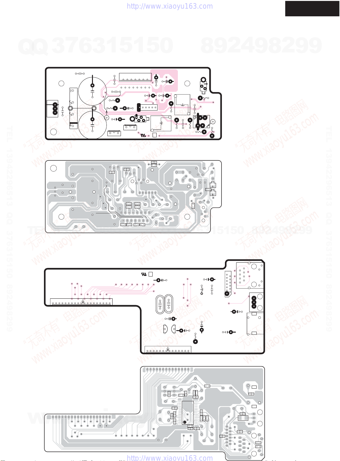
PRINTED CIRCUIT BOARD VIEW - 1
NC-500
U000:AF-7660
Q
Q
TEL 13942296513 QQ 376315150 892498299
7
3
Component side
P503B
Soldering side
C906
6
C905
D905
C914
C913
3
P510
J502
J503A
C914
C913
1
C507
C508
R913
R914
C916
Q902
C918
J501
5
J503B
C915
Q901
C917
R503
R501
1
Q501
P505A
R506
R508
5
C501
P504A
L501
3
R513
0
C502
C505
C506
R524
25137660
NCAF-7660
C513
L501
L502
L502
R526
C512
C511
R525
8
P552A
R355
P502B
P507B
R356
R523
R510
Q503
R509
9
Q504
2
4
9
8
2
9
9
TEL 13942296513 QQ 376315150 892498299
TEL
U003:VD-7654
w
13942296513
Component side
Soldering side
w
w
.
xia
P102A
R507
o
R504R505
y
R502
NCVD-7654
1
X271
P306A
u
Q
25137654
C282
Q275
1
Q
C285
C270
C295
3
X281
C296
C289
Q274
R294
C298
6
1
R276
C272
C288
7
R293
C283
C290
Q271
3
C273
6
L271
9
9
2
8
9
4
2
9
8
0
5
1
5
1
3
P601
C275
C276
P608A
C992
C297
C256
R296
R256
R292
Q271
C274
R275
R274
.
R273
c
C995
C991
o
L991
C994
P601
U701
U701
P251
P251
C299
m
R991
R992
Page 15
PRINTED CIRCIT BOARD VIEW - 2-1
U001:DG7651
Q
Q
3
Component side
6
7
TEL 13942296513 QQ 376315150 892498299
TEL
13942296513
3
1
5
R952
Q905
C953
1
D7005
C952
C957
R951
R923
P7003B
C959
R953
Q905
C956
C955
P7004B
C958
C951
R904
R906
R924
C961
D901
C907
5
C954
Q908
P606A
C962
P308B
Q304
R325
Q307
R327
0
P7001A
R7389
R7390
R7397
R7297
R7220
R7228
R7003
Q308
C7297
1
C7001
C7295
C7206
C933
Q906
Q700
R7225
Q907
C7203
X781
3
R7295
1
R7290
R7289
Q700
C781
D781
R7395
Q904
L951
C7204
Q323
Q7002
C908
R915
R7206
R7212
C962
R7205
X7201
Q
R320
Q909
R326
R328
Q324
C7205
1
C7213
D7003
Q
C908
C934
R965
D7004
C7002
R912
R964
L951
R7201
R7202
R7203
D951
C910
C968
P913A
R922
R905
P504B
8
3
R7288
R7287
R7292
R7291
R7294
R7277
R7272
R7269
R7268
25137651C
NCDG-7651
R7266
R7239
R7231
R7232
R7230
C7202
R7002
R784
Q781
R783
6
7
C784 C785
R102
Q102
C108
Q101
C106
C107
R110
Q104
C104
R786
C782
Q781
Q103
R7286
R7278
R7255
R785
3
R7494
R114
R103
R782
R109
C105
R7285
C7294
R7257
R7256
R7243
R7242
R7240
R7284
R7267
R7260
R7248
R7247
R7245
R7244
R101
R7283
R781
1
C103
R111
R108
9
R7281
R7282
R7394
R7493
R7279
C7003
C786
5
R107
R113
R7280
R7391
C703
C7291
R7270 R7271
R112
R704
R7263
R7249
C102
C101
R105
R104
X703
1
R7259
R106
1
P101B
R7274
2
R01
R710
Q714
C706
5
R708
R709
R705
C702
P610A
0
4
P01
R706
R707
P702
P102B
9
8
9
2
8
4
2
9
8
NC-500
9
9
2
9
TEL 13942296513 QQ 376315150 892498299
9
w
w
w
.
xia
E7001
R310
C307
R305
R306
o
R323
R317
R321
Q302
C305
y
C329
C327
R313
C321
R318
R324
C330
1
R311
C306
u
R312
R314
R322
1
C304
C302
R302
C322
Q301
C328
C303
Q301
R301
6
R307
R309
C301
3
R308
E7002
.
c
o
m
Page 16
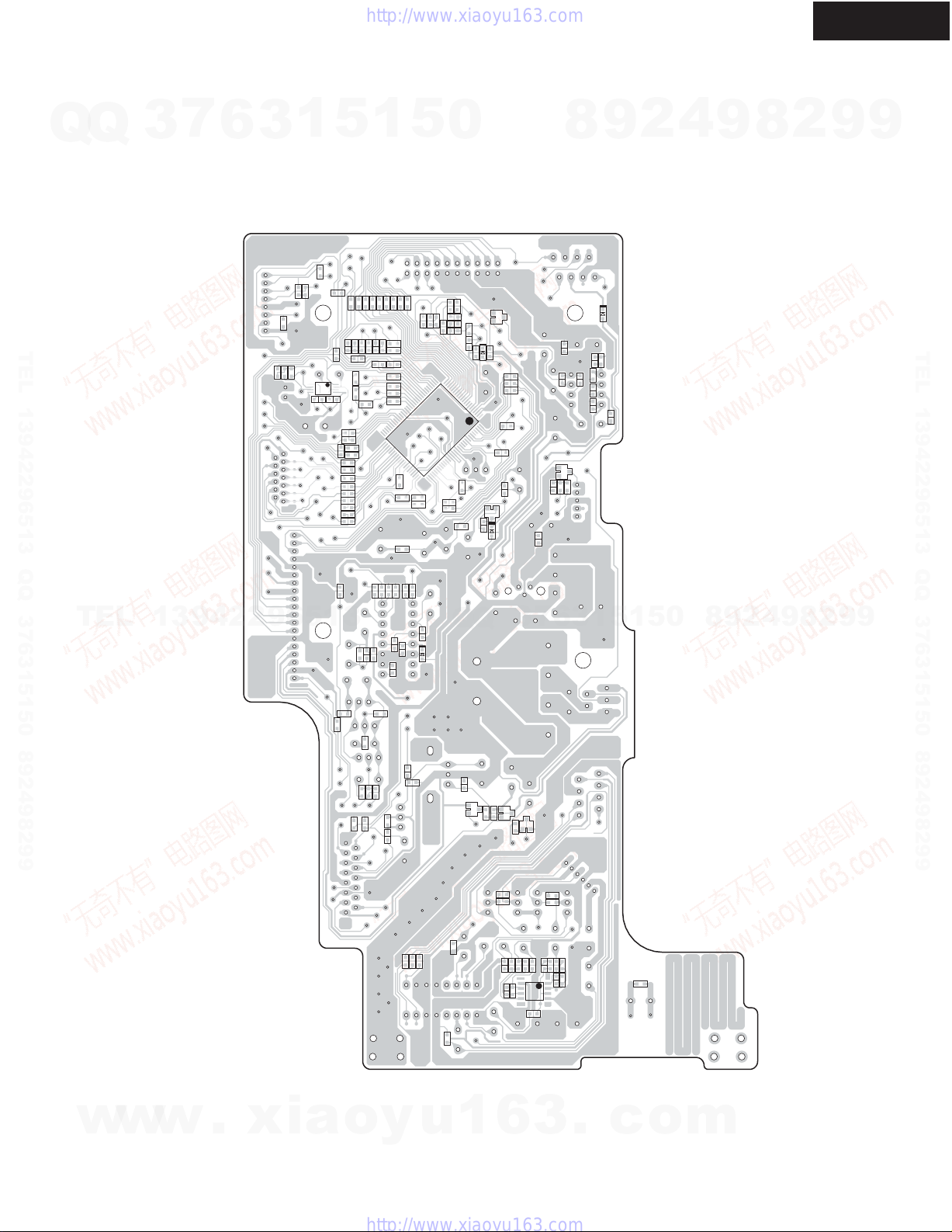
PRINTED CIRCUIT VIEW 2 - 2
NC-500
Q
U001:DG-7651
Q
3
7
6
3
1
5
1
5
0
Soldering side
R01
R708
R710
R704
R7280
R7281
R7282
R7283
R7284
R7285
R7286
C7294
R7288
R709
TEL 13942296513 QQ 376315150 892498299
R706
R707
R705
C706
Q714
R7263
R7249
R7274
R106
1
C703
R7259
C7291
R7279
R7270 R7271
R7391
R7493
R7267
R7260
R7248
R7247
R7245
R7244
R7243
R7242
R7240
R7257
R7256
R7394
R7278
R7255
R7287
R7494
R7291
R7294
R7277
R7272
R7269
R7268
R7266
R7239
R7231
R7232
R7230
R7002
R784
R786
R785
R781
R782
R7292
R7389
R7390
R7290
R7395
R7289
C7295
C7206
R7295
Q7001
Q7001
R7228
R7225
R7003
R783
C7297
R7397
R7297
R7220
D7004
1
C7002
R7212
C7213
D7003
R7206
Q7002
R7205
Q904
R7201
R7202
R7203
C910
C968
8
C958
C954
Q908
R906
9
D7005
2
4
9
8
2
9
9
TEL 13942296513 QQ 376315150 892498299
C959
R952
R953
C956
C955
C953
C957
R904
TEL
13942296513
R105
R104
C782
C103
R107
C784 C785
R111
R102
R114
R113
R103
R101
R109
R112
R108
C105
Q
C781
D781
C106
R110
R308
R309
C933
R965
R964
Q906
R307
R302
R301
Q304
R320
Q909
R326
R328
C322
C328
R325
R327
R312
R322
R311
R323
R313
R314
C321
R318
R324
R317
1
R321
C327
Q302
R310
9
9
2
8
9
4
2
9
8
0
5
1
5
1
3
6
7
3
Q
w
w
w
.
xia
o
y
u
1
6
3
.
c
o
m
Page 17

PRINTED CIRCUIT BOARD VIEW - 3
NC-500
Q
U002:AF-7653
Q
3
7
6
3
1
5
1
5
0
Component side
E501
Q910
Q910
C904
TEL 13942296513 QQ 376315150 892498299
25137653
NCAF-7653
3
P306B
P907
C909
P507A
Q311
C210
Q312
P907
R918
C204
P602A
C202
C206
C205
P506
C357
C211
C203
C209
C212
P506
R225
R226
Q309
Q310
C201
C358
P505B
C371
R366
84
C3
P308A
8
RL501RL501
C521
Q502
P501
9
P501
P502A
2
4
9
8
2
9
9
TEL 13942296513 QQ 376315150 892498299
TEL
13942296513
Soldering side
Q505
R515
R514
R204
R206
R216
R222
R220
R303
Q911
Q912
Q305
R920
R316
R919
R921
R315
C990
9
9
2
8
9
4
2
9
8
0
5
1
5
1
3
6
7
3
Q
Q
R202
Q201
R208
R214
R212
R218
Q305
R304
R333
R332
1
R370
R203
R207
R205
Q203
R334
R369
Q202
R223
R342
R211
R213
R215
Q303
1
R339
C394
R201
R217
R219
R221
R364
R363
Q313
D302
D301
D501
R340
C393
R341
R368
R367
C524
R371
R372
C523
1
R209
R210
1
1
R224
R331
C351
C352
C392
C391
C390
w
w
w
.
xia
o
y
u
1
6
3
.
c
o
m
Page 18

PRINTED CIRCUIT BOARD VIEW - 4
NC-500
7
3
Q
Q
TEL 13942296513 QQ 376315150 892498299
TEL
U004:PS-7655
Component side
T901
13942296513
E901
916
R
P928A
6
C920
P503A
P929A
R
917
L901
R907
3
P927
C901
223 OR6
T901
R908
R909
1
L901
C903
AC-G
AC-H
R902
P7003A
RL901
5
AC-G AC-H
P901A
P926A
RISK OF FIRE
R901
1
P922A
C902
FUSE
-REPLACE
AS MARKED
5
1.25A/125V
T400mAL250V
F902A
F902
F902B
NCPS-
25137655
7655
3
RL901
P924
F901A
F901
F901B
P923A
0
P921A
Q
Q
Soldering side
7
3
8
6
3
9
1
D902
5
1
2
R910
5
4
C921
D913
0
D912
8
9
D911
9
8
2
4
2
9
8
9
2
9
9
TEL 13942296513 QQ 376315150 892498299
9
w
w
U005:DIS-7656
Component side Soldering side
P551
1
NCDIS-7656
25137656
P554
S7002
S7001
P553
C7010
D7001
xia
P7004A
P552B
P7006B
R7013
o
y
u
1
6
w
P551
U7001
.
C550
3
R7001
.
C552
C551
R7012
C7011
c
o
m
Page 19

PRINTED CIRCUIT BOARD VIEW - 5
NC-500
7
Q
Q
TEL 13942296513 QQ 376315150 892498299
3
U006:ETC-7657
Component side Soldering side
6
2
S7016
2
S7011
P7006A
2
2
S7014
S7015
U007:PS-7658
Component side Soldering side
3
2
S7012
1
S7018
2
S7013
5
1
5
0
2
S7017
2
S7006
25137657
NCETC-7657
S7005
2
2
2
S7003
2
S7007
1
2
S7004
8
R7017
R7015
R7014
R7016
9
2
R7008
4
R7007
R7010
R7004
9
R7006
R7005
8
R7009
2
9
9
TEL 13942296513 QQ 376315150 892498299
TEL
NCETC-7659
25137659
NCPS-765825137658
P901B
1
13942296513
U008:ETC-7659
Component side Soldering side
P928
P921
P926
S901
P922
9
9
2
8
9
4
2
9
8
0
5
1
5
1
3
6
7
3
Q
Q
P923
S901
1
P901B
P929
AC230VAC120V
P927A
HL
w
w
w
.
xia
o
y
u
1
6
3
.
c
o
m
Page 20

PRINTED CIRCUIT BOARD VIEW - 6
U009:DG-7662, Network Circuit
Q
Q
3
7
6
3
1
5
1
5
0
8
9
2
4
9
8
2
NC-500
9
9
TEL 13942296513 QQ 376315150 892498299
TEL
13942296513
Q
Q
3
7
6
3
1
5
1
5
0
8
9
2
4
9
8
2
9
TEL 13942296513 QQ 376315150 892498299
9
w
w
w
.
xia
o
y
u
1
6
3
.
c
o
m
Page 21

PRINTED CIRCUIT BOARD VIEW - 3
NC-500
Q
U002:AF-7653
Q
3
7
6
3
1
5
1
5
0
Component side
E501
Q910
Q910
C904
TEL 13942296513 QQ 376315150 892498299
25137653
NCAF-7653
3
P306B
P907
C909
P507A
Q311
C210
Q312
P907
R918
C204
P602A
C202
C206
C205
P506
C357
C211
C203
C209
C212
P506
R225
R226
Q309
Q310
C201
C358
P505B
C371
R366
84
C3
P308A
8
RL501RL501
C521
Q502
P501
9
P501
P502A
2
4
9
8
2
9
9
TEL 13942296513 QQ 376315150 892498299
TEL
13942296513
Soldering side
Q505
R515
R514
R204
R206
R216
R222
R220
R303
Q911
Q912
Q305
R920
R316
R919
R921
R315
C990
9
9
2
8
9
4
2
9
8
0
5
1
5
1
3
6
7
3
Q
Q
R202
Q201
R208
R214
R212
R218
Q305
R304
R333
R332
1
R370
R203
R207
R205
Q203
R223
R334
R369
Q202
R342
R211
R213
R215
Q303
1
R339
C394
R201
R217
R219
R221
R364
R363
Q313
D302
D301
D501
R340
C393
R341
R368
R367
C524
R371
R372
C523
1
R209
R210
1
1
R224
R331
C351
C352
C392
C391
C390
w
w
w
.
xia
o
y
u
1
6
3
.
c
o
m
Page 22

PRINTED CIRCUIT BOARD VIEW - 4
NC-500
7
3
Q
Q
TEL 13942296513 QQ 376315150 892498299
TEL
U004:PS-7655
Component side
T901
13942296513
E901
916
R
P928A
6
C920
P503A
P929A
R
917
L901
R907
3
P927
C901
223 OR6
T901
R908
R909
1
L901
C903
AC-G
AC-H
R902
P7003A
RL901
5
AC-G AC-H
P901A
P926A
RISK OF FIRE
R901
1
P922A
C902
FUSE
-REPLACE
AS MARKED
5
1.25A/125V
T400mAL250V
F902A
F902
F902B
NCPS-
25137655
7655
3
RL901
P924
F901A
F901
F901B
P923A
0
P921A
Q
Q
Soldering side
7
3
8
6
3
9
1
D902
5
1
2
R910
5
4
C921
D913
0
D912
8
9
D911
9
8
2
4
2
9
8
9
2
9
9
TEL 13942296513 QQ 376315150 892498299
9
w
w
U005:DIS-7656
Component side Soldering side
P551
1
NCDIS-7656
25137656
P554
S7002
S7001
P553
C7010
D7001
xia
P7004A
P552B
P7006B
R7013
o
y
u
1
6
w
P551
U7001
.
C550
3
R7001
.
C552
C551
R7012
C7011
c
o
m
Page 23

PRINTED CIRCUIT BOARD VIEW - 5
NC-500
7
Q
Q
TEL 13942296513 QQ 376315150 892498299
3
U006:ETC-7657
Component side Soldering side
6
2
S7016
2
S7011
P7006A
2
2
S7014
S7015
U007:PS-7658
Component side Soldering side
3
2
S7012
1
S7018
2
S7013
5
1
5
0
2
S7017
2
S7006
25137657
NCETC-7657
S7005
2
2
2
S7003
2
S7007
1
2
S7004
8
R7017
R7015
R7014
R7016
9
2
R7008
4
R7007
R7010
R7004
9
R7006
R7005
8
R7009
2
9
9
TEL 13942296513 QQ 376315150 892498299
TEL
NCETC-7659
25137659
NCPS-765825137658
P901B
1
13942296513
U008:ETC-7659
Component side Soldering side
P928
P921
P926
S901
P922
9
9
2
8
9
4
2
9
8
0
5
1
5
1
3
6
7
3
Q
Q
P923
S901
1
P901B
P929
AC230VAC120V
P927A
HL
w
w
w
.
xia
o
y
u
1
6
3
.
c
o
m
Page 24

PRINTED CIRCUIT BOARD VIEW - 6
U009:DG-7662, Network Circuit
Q
Q
3
7
6
3
1
5
1
5
0
8
9
2
4
9
8
2
NC-500
9
9
TEL 13942296513 QQ 376315150 892498299
TEL
13942296513
Q
Q
3
7
6
3
1
5
1
5
0
8
9
2
4
9
8
2
9
TEL 13942296513 QQ 376315150 892498299
9
w
w
w
.
xia
o
y
u
1
6
3
.
c
o
m
Page 25

BLOCK DIAGRAM AND DESCRIPTION OF IC - 1
NC-500
7
Q
Q
TEL 13942296513 QQ 376315150 892498299
3
Q305:TC4052B
ANALOG SWITCH
6
3
1
5
1
5
0
4
2
9
8
~SELB ~SELA INPUT
H H NO USE
H L NETWORK
L H TUNER
L L AUX
9
8
2
9
9
TEL 13942296513 QQ 376315150 892498299
TEL
13942296513
Q
Q
3
7
6
3
1
5
1
5
0
8
9
2
4
9
8
2
9
9
w
w
w
.
xia
o
y
u
1
6
3
.
c
o
m
Page 26

BLOCK DIAGRAM AND DESCRIPTION OF IC - 6
Q781:BU1923
7
Q
Q
TEL 13942296513 QQ 376315150 892498299
3
RDS DECODER
Block diagram
2.2 F
6
MUX
270p
Vref
V
1
SS1
V
DD1
3
(4)
120k
(3)
(5)
Power supply
(6)
1
Analog
100k
100k
5
1
anti-aliasing
filter
5
0
8
8th Switched
capacitor filter
9
2
SS3
V
4
9
560p
(7) (8)
comparator
CMP
8
(16)
(1)
RCLK
QUAL
2
NC-500
9
9
TEL 13942296513 QQ 376315150 892498299
TEL
V
2
V
DD2
SS2
(12)
Digital
Power supply
(11)
(13) (14) (10)
XI
4.332MH
Z
33pF
3
33pF
3
RCLK
1
QUAL
1
13942296513
PLL
57kH
Z
RDS/ARI
XO
Reference
clock
(N.C.)
2
RDATA
RDATA
6
3
Bi-phase
decoder
1
SS2
V
6
SS1
V
1
5
Measurement
T1
10111213141516
5
circuit
T1
7
SS3
V
0
(9)
T2
Differential
decoder
8
T2
9
8
CMP
PLL
1187.5Hz
7
3
Q
Q
1 : VDD1 and VDD2 are separated within the IC.
2 : Have VDD2 (digital power supply) of a sufficiently low impedance.
3 : Match the capacitor constants with the crystal manufacturer.
XO
3
Vref
XI
4
MUX
DD2
V
5
DD1
V
9
2
(2)
9
9
2
8
9
4
w
w
w
.
xia
o
y
u
1
6
3
.
c
o
m
Page 27

BLOCK DIAGRAM AND DESCRIPTION OF IC - 6
Q781:BU1923
7
Q
Q
TEL 13942296513 QQ 376315150 892498299
3
RDS DECODER
Pin descriptions
Pin No. Pin nameSymbol Functions Input/Output type
10 T1
11 V
12 V
13 XI
14 XO
15
16 RCLK Demodulator clock 1187.5Hz clock (refer to the timing diagram)
6
1 QUAL Demodulator quality Type CGood data : High, bad data : Low
2 RDATA Demodulator data
3 Vref Reference voltage
4 MUX Input
D
5V
6V
7
8
9T2
D1
S
S1
S
S3
V
CMP Comparator input Type D
SS2
DD2
(N.C.)
1
5
1
3
Analog power supply
GND
Test input Type BOpen or connected to ground
Digital power supply
Crystal oscillator Type A
5
0
Refer to output data timing
1/2 V
DD1
(refer to input/output circuits)
Composite signal input (refer to input/output circuits)
4.5V to 5.5V
C-junction (refer to input/output circuits )
4.5V to 5.5V
Connects to 4.332MHz oscillator
(refer to input/output circuits)
8
9
2
4
9
Type E
Type D
Type C
8
2
NC-500
9
9
TEL 13942296513 QQ 376315150 892498299
TEL
13942296513
Input / Output circuits
Type A Type B
10M
Type D
Type E
Q
Q
3
7
6
3
1
Type C
Type F
5
1
VREF
5
0
8
9
2
4
9
8
2
9
9
w
w
w
.
xia
o
y
u
1
6
3
.
c
o
m
Page 28

BLOCK DIAGRAM AND DESCRIPTION OF IC - 5
Q714:S-3531A
Q
Q
7
3
REAL-TIME CLOCK
6
3
1
5
1
5
0
8
9
2
4
9
8
2
NC-500
9
9
TEL 13942296513 QQ 376315150 892498299
TEL
13942296513
Q
Q
3
7
6
3
1
5
1
5
0
8
9
2
4
9
8
2
9
TEL 13942296513 QQ 376315150 892498299
9
w
w
w
.
xia
o
y
u
1
6
3
.
c
o
m
Page 29

BLOCK DIAGRAM AND DESCRIPTION OF IC - 5
Q714:S-3531A
Q
Q
7
3
REAL-TIME CLOCK
6
3
1
5
1
5
0
8
9
2
4
9
8
2
NC-500
9
9
TEL 13942296513 QQ 376315150 892498299
TEL
13942296513
Q
Q
3
7
6
3
1
5
1
5
0
8
9
2
4
9
8
2
9
TEL 13942296513 QQ 376315150 892498299
9
w
w
w
.
xia
o
y
u
1
6
3
.
c
o
m
Page 30

BLOCK DIAGRAM AND DESCRIPTION OF IC - 4
Q605:WM8716
Q
Q
3
DAC
7
6
3
1
5
1
5
0
8
9
2
4
9
8
2
NC-500
9
9
TEL 13942296513 QQ 376315150 892498299
TEL
13942296513
Q
Q
3
7
6
3
1
5
1
5
0
8
9
2
4
9
8
2
9
TEL 13942296513 QQ 376315150 892498299
9
w
w
w
.
xia
o
y
u
1
6
3
.
c
o
m
Page 31

BLOCK DIAGRAM AND DESCRIPTION OF IC - 4
Q605:WM8716
Q
Q
3
DAC
7
6
3
1
5
1
5
0
8
9
2
4
9
8
2
NC-500
9
9
TEL 13942296513 QQ 376315150 892498299
TEL
13942296513
Q
Q
3
7
6
3
1
5
1
5
0
8
9
2
4
9
8
2
9
TEL 13942296513 QQ 376315150 892498299
9
w
w
w
.
xia
o
y
u
1
6
3
.
c
o
m
Page 32

BLOCK DIAGRAM AND DESCRIPTION - 3
NC-500
7
Q
Q
TEL 13942296513 QQ 376315150 892498299
3
Q271:LC74761M-9845
ON-SCREEN DISPLAY LSI
6
3
1
5
1
5
0
8
9
2
4
9
8
2
9
9
TEL 13942296513 QQ 376315150 892498299
TEL
13942296513
Pin Assignment
Q
Q
3
7
6
3
1
5
1
5
0
8
9
2
4
9
8
2
9
9
w
w
w
.
xia
o
y
u
1
6
3
.
c
o
Top view
m
Page 33

BLOCK DIAGRAM AND DESCRIPTION OF IC - 3
Q271:LC74761M-9845
7
Q
Q
TEL 13942296513 QQ 376315150 892498299
TEL
3
ON-SCREEN DISPLAY LSI
Pin Functions
Pin No. Symbol Function Description
1V
2 Xtal
3 Xtal
4 HSYNC
5 Xtal
6 Xtal
7 VSYNC
8 CS Enable input
9 SIN Data input Serial data input (hysteresis input). Pull-up resistor built in (metal option).
10 SCLK Clock input Clock input for serial data input (hysteresis input). Pull-up resistor built in (metal option).
11 SECAM
12 525/625
13 NTSC/PAL
13942296513
14 3.58/4.43 3.58/4.43 switch input/output During output, functions as general output port or half-tone output (command switch).
15 RST Reset input
16 CV
17 V
18 CV
19 CV
20 SYNC
21 SEP
22 V
23 PD
24 AMP
25 AMP
26 FC Control voltage input AFC control voltage input
27 VCO
28 VCO
29 SYNC
30 V
6
SS
IN1
OUT1
OUT
IN2
OUT2
OUT
OUT
DD2
IN
CR
IN
C
SS
OUT
IN
OUT
IN
OUT
DET
DD1
1
5
1
3
Ground Ground connection
Crystal oscillator connection
Horizontal synchronization Outputs the horizontal synchronization signal (AFC). The output polarity can be selected
output (metal option). Also functions as general output port (command switch).
Crystal oscillator connection
Vertical synchronization output
SECAM mode switch input/
output (command switch)
525/625 switch input/output
(command switch)
NTSC/PAL switch input/output
(command switch)
(command switch) Low = 3.58, high = 4.43
Video signal output Composite video output
Power supply connection Power supply connection for composite video signal level generation
Video signal input Composite video input
Video signal input SECAM chroma signal input
Sync separator circuit input Built-in sync separator circuit video signal input
Sync separator circuit Built-in sync separator circuit
Ground Ground connection
Control voltage output AFC control voltage output
AFC filter connection Filter connection
LC oscillator connection VCO LC oscillator circuit coil and capacitor connection
External synchronization signal
detection output
Power supply connection Power supply connection (+5 V: digital system power supply)
5
0
Connection for the crystal and capacitor used to form the crystal oscillator that generates
the internal synchronization signal. The oscillator can be selected with a command switch.
Connection for the crystal and capacitor used to form the crystal oscillator that generates
the internal synchronization signal.
Outputs the vertical synchronization signal. The output polarity can be selected (metal
option). Also functions as general output port (command switch).
Enables/disables serial data input. Serial data is enabled when this pin is low (hysteresis
input). Pull-up resistor built in (metal option).
During input, switches between SECAM and other modes.
During output, functions as general output port or internal V output (command switch).
Low = other modes, high = SECAM mode
During input, switches between 525 scan lines and 625 scan lines.
During output, functions as general output port or character data output (command switch).
Low = 525 lines, high = 625 lines
Switches the color mode between NTSC and PAL.
During output, functions as general output port or frame data output (command switch).
Low = NTSC, high = PAL
3
Q
Q
Switch FSC between 3.58 MHz and 4.43 MHz.
System reset input pin, low is active (hysteresis input).
Pull-up resistor built in (metal option).
Outputs the exclusive NOR of the horizontal synchronization signal (AFC) and CSYNC (sync
separator). The output polarity can be selected (metal option). Also functions as general
output port (command switch).
7
8
6
3
1
9
5
2
1
5
0
4
9
8
9
2
8
4
2
9
8
NC-500
9
9
2
9
TEL 13942296513 QQ 376315150 892498299
9
w
w
w
.
xia
o
y
u
1
6
3
.
c
o
m
Page 34

BLOCK DIAGRAM AND DESCRIPTION OF IC - 2
NC-500
7
Q
Q
TEL 13942296513 QQ 376315150 892498299
3
Q301:TC9413AP
ELECTRONIC VOLUME CONTROL
6
3
1
5
1
5
0
8
9
2
4
9
8
2
9
9
TEL 13942296513 QQ 376315150 892498299
TEL
13942296513
Q
Q
3
7
6
3
1
5
1
5
0
8
9
2
4
9
8
2
9
9
w
w
w
.
xia
o
y
u
1
6
3
.
c
o
m
Page 35

BLOCK DIAGRAM AND PIN DESCRIPTION OF IC - 7
Q611:AK4353
Q
Q
7
3
DAC WITH DIT
Block Diagram
6
3
1
CAD0CAD1
5
I2C
1
5
CCLK CDTICSN
0
MC K I
8
9
MC K O
2
4
9
8
2
NC-500
9
9
TX
TEL 13942296513 QQ 376315150 892498299
TEL
LRCK
BICK
SDTI
TTL
DVDD
DVS S
DZF
13942296513
DIT
Serial Input
Interfac e
Mixer
PDN
3-wire Serial Control Mode (I2C = “ L”)
I2C
CAD0CAD1
ATT
ATT
8X
Interpolator
8X
Interpolator
Q
Q
SCL SDACSN
Clock G enerator
3
DS
Modulator
DS
Modulator
3
6
7
MC K I
5
1
MC K O
1
5
LPF
LPF
0
8
9
AV DD
AV S S
VCOM
AOUTL
AOUTR
4
2
9
8
2
9
TEL 13942296513 QQ 376315150 892498299
9
w
w
w
TX
LRCK
BICK
SDTI
TTL
DVDD
DVS S
DZF
.
DIT
Serial Input
Interfac e
Mixer
PDN
xia
Clock G enerator
y
8X
Interpolator
8X
Interpolator
u
1
6
ATT
ATT
I2C Bus Control Mode (I2C = “H”)
o
DS
Modulator
DS
Modulator
3
.
c
LPF
LPF
o
AV DD
AV S S
VCOM
AOUTL
AOUTR
m
Page 36

BLOCK DIAGRAM AND PIN DESCRIPTION OF IC - 7
Q611:AK4353
Q
Q
7
3
DAC WITH DIT
Pin Layout
6
3
1
5
1
5
0
8
9
2
4
9
8
2
NC-500
9
9
10
11
12
1
2
3
4
5
6
7
8
9
Top
View
Q
Q
3
MCKO
TX
TEL 13942296513 QQ 376315150 892498299
TEL
DVDD
DVSS
MCKI
BICK
SDTI
LRCK
PDN
13942296513
CSN
SCL/CCLK
SDA/CDTI
7
6
3
1
24
23
22
21
20
19
18
17
16
15
14
13
5
1
5
DZF
NC
AVDD
AVSS
VCOM
AOUTL
AOUTR
CAD1
CAD0
0
I2C
TTL
TST
8
9
2
4
9
8
2
9
TEL 13942296513 QQ 376315150 892498299
9
w
w
w
.
xia
o
y
u
1
6
3
.
c
o
m
Page 37

BLOCK DIAGRAM AND PIN DESCRIPTION OF IC - 7
Q611:AK4353
7
Q
Q
TEL 13942296513 QQ 376315150 892498299
TEL
3
DAC WITH DIT
No. Pin Name I/O Description
1 MCKO O Master Clock Output Pin
2TX O
3 DVDD 4 DVSS 5MCKI I
6BICK I
7 SDTI I
8LRCK I
9 PDN I Power-Down Pin
10 CSN I Chip Select Pin at 3-wire Serial control mode
13 TST I Test pin
13942296513
14 TTL I Digital Input Level Select Pin
15 I2C I Control Mode Select Pin
16 CAD0 I
17 CAD1 I
18 AOUTR O
19 AOUTL O
20 VCOM O Common Voltage Output Pin, AVDD/2
21 AVSS 22 AVDD 23 NC - No Connect
24 DZF O Zero Input Detect Pin
6
SCL I Control Clock Pin at I
CCLK I
SDA I/O Control Data Input/Output Pin at I2C Bus control mode12
CDTI I
3
1
5
1
5
0
PIN/FUNCTION
Same frequency as MCKI is output
Transmit Channel Output Pin
Digital Power Supply Pin, +2.7∼
Digital Ground Pin, 0V
Master Clock Input Pin
Serial Data Clock Pin
Serial Data Input Pin
Serial Input Channel Clock Pin
When “L”, the circuit is in power-down mode.
The AK4353 should always be reset upon power-up.
This pin should be connected to DVDD at I
Control Clock Pin at 3-wire serial control mode
Control Data Input Pin at 3-wire serial control mode
This pin should be connected to DVDD.
“L”: CMOS, “H”: TT
“L”: 3-wire Serial, “H”: I
Chip Address Select 0 Pin
Chip Address Select 1 Pin
Rch Analog Output Pin
Lch Analog Output Pin
Used for analog common voltage.
Large external capacitor is used to reduce power supply noise.
Analog Ground Pin
Analog Power Supply Pin
Nothing should be connected externally to this pin.
When SDTI follows a total 8192 LRCK cycles with “0” input data
or RSTN = “0”, this pin goes to “H”
Q
2
Q
C bus control mode11
3
L
2
C Bus
+5.5V
7
8
6
3
.
2
9
2
C Bus control mode.
5
1
5
1
0
4
9
8
9
2
8
4
2
9
8
NC-500
9
9
2
9
TEL 13942296513 QQ 376315150 892498299
9
w
w
w
.
xia
o
y
u
1
6
3
.
c
o
m
Page 38

DESCRIPTION OF MAIN MICROPROCESSOR - 1
NAC-2.3
Q7001, M30624FGAFP
Q
Q
No. Symbol I/O Act. Description (Function)
1 OSDDA O H Data of OSD communication
2 OSDCL O CLK Clock of OSD communication
3 ~OSDCS O L To select OSD communication
4,5 - O 6 ~IRIN I L Inflared signal from rear panel (IR IN)
7 ~IRMAIN I L Inflared signal from front panel
TEL 13942296513 QQ 376315150 892498299
8 BYTE I H VSS
9 CNVSS I H Change of prosessor mode
10,11 - O 12 ~RESET I L Reset
13 XOUT O Crystal oscillator, connect to 16MHz oscillator
14 VSS GND
15 XIN I Crystal oscillator, connect to 16MHz oscillator
16 VCC Power supply, 5V
17 ~NMI I L 18 - O 19 RDSCLK I CLK RDS clock
20 ~POFF I L Detect power failure
21~24 - O -
TEL
25 STBLED O H STANDBY LED
26 - O 27 ~FLPOWER O L Control of FL power supply
28 ~FLTEST O L FL tube test
29 RTCSCL O CLK Clock of RTC IC
30 RTCSDA I/O H Data of RTC IC
31~34 - O 35 NETTX O L Communication of network microprocessor
36 NETRX I L Communication of network microprocessor
37 - O 38 ~ETPOWER O L Control of power supply for ETHER IC
39 ~DITPD O L DIT power down
40 ~DITCS O L To select DIT
41 (~EPM) I L Connect to VSS
42 - O 43 XPOR O L EP7312 reset
44 ~DARST O L DAC reset
45 DACS O L To select DAC
46 (~CE) I L Connect to Vcc
47 DIGCL O CLK Common clock of DIT/DAC
48 DAMUT O L Muting of DAC
49 DIGDO O H Common data of DIT/DAC
50~54 - O -
w
w
55 VOLDA O H Serial data of TC9412 volume IC
56 VOLCL O CLK Serial clock of TC9412 volume IC
7
3
13942296513
w
6
.
xia
3
1
5
o
1
y
5
u
0
Q
1
Q
3
6
3
7
8
6
3
.
1
9
5
c
2
1
0
5
o
4
8
m
9
9
2
8
4
2
9
8
2
9
9
9
TEL 13942296513 QQ 376315150 892498299
9
Page 39

DESCRIPTION OF MAIN MICROPROCESSOR - 2
NAC-2.3
Q7001, M30624FGAFP
Q
Q
No. Symbol I/O Act. Description (Function)
57 VOLSTB O H Strobe ofTC9412 volume IC
58 - O 59 AMUT O H Analog muting
60 TUMUT O H Tuner muting
61 - O 62 VCC Power supply, 5V
TEL 13942296513 QQ 376315150 892498299
63 SPRLY O H Speaker relay
64 VSS GND
65 - O 66 ~STEREO I L Detect STEREO of tuner
67 ~SD I L Detect SD of tuner
68 PLLCL O CLK PLL clock of tuner
69 PLLCS O H To select of PLL of tuner
70 PLLDA O H PLL data of tuner
71 RDSSIG I H RDS signal
72 RDSDA I H RDS data
73 ~RTCINT I L Interruption signal (1Hz) from RTC IC
74 FLBUSY I L FL tube busy
75,76 - O -
TEL
77 ~SELA O L TC4052 function change, the reversal output terminal of A
78 ~SELB O L TC4052 function change, the reversal output terminal of B
79 FLWR O H FL tube WR
80 ~FLSEL O L FL tube ~SEL
81 FLDA7 O H FL tube data 7
82 FLDA6 O H FL tube data 6
83 FLDA5 O H FL tube data 5
84 FLDA4 O H FL tube data 4
85 FLDA3 O H FL tube data 3
86 FLDA2 O H FL tube data 2
87 FLDA1 O H FL tube data 1
88 FLDA0 O H FL tube data 0
89 RDSEN I H To select of RDS function
90 AREA2 I H Local setting 2
91 AREA1 I H Local setting 1
92 HPDET I H Detect headphone (Insert : "H")
93 - O 94 MODEL I H(AD) Model setting
95 KEY1 I AD Key 1
96 AVSS A/D convertor power supply, connect to VSS
97 KEY0 I AD Key 0
98 VREF I Reference voltage of A/D convertor
99 AVCC A/D convertor power supply, connect to Vcc
w
w
100 - O -
7
3
13942296513
w
6
.
xia
3
1
5
o
1
y
5
u
0
Q
1
Q
3
6
3
7
8
6
3
.
1
9
5
c
2
1
0
5
o
4
8
m
9
9
2
8
4
2
9
8
2
9
9
9
TEL 13942296513 QQ 376315150 892498299
9
Page 40

ADJUSTMENT & CONFIRMATIONS OF OPERATIONS
NC-500
Q
TEL 13942296513 QQ 376315150 892498299
ADJUSTMENT OF FREQUENCY
Q
a) Turn C702 CCW to set minimum position before POWER ON.
b) Set the frequency at P702 to 32768Hz by adjusting C702 under the condition of no input and no load,
immediately after POWER ON.
c) After 4 ~ 6 minutes of heat running, re-adjust by following b.
OPERATIONS OF SPEAKER RELAYS
The relay shall be ON about 5 seconds after POWER is ON and shall be OFF immediately after
POWER is OFF.
INITIAL SETTING FOR SHIPPING
1. Initialization of memories
Press STANDBY/ON button while pressing down INPUT button when the unit is POWER ON,
2. Other settings
Pull out the AC cord at the standby mode.
7
3
then the FLT displays "CLEAR", and turn to STAND-BY. Remove power cord from power line.
6
3
1
5
1
5
0
8
9
2
4
9
8
2
9
9
TEL 13942296513 QQ 376315150 892498299
TEL
13942296513
Q
Q
3
7
6
3
1
5
1
5
0
8
9
2
4
9
8
2
9
9
w
w
w
.
xia
o
y
u
1
6
3
.
c
o
m
Page 41

FIRMWARE UPDATE - 1
NC-500
7
Q
Q
1
2 Make the folder of a suitable name (ex.:FWNC500) in that.
3 Putting the following 4 files in that.
Fdist.fdf - File Distribution File
FW_0_1_0.dcf - Device Construciton File
LanY08na.mot - The program of Network microprocessor (The file name changes by the version).
LanY08rb(L).mot - The program of System microprocessor (The file name changes by the version)
TEL 13942296513 QQ 376315150 892498299
4 Start Net-Tune Central.
Update initializes each setting data.
Put only the folder which puts firmware in the firmware folder. And, do not make the folder of the subordinate position from it.
When you replaces or edits the above file, you should end Net-Tune Central once, and restart. Otherwise, the change is not reflected.
TEL
3
Arrangements for PC
Make the firmware folder under the Net-Tune Central folder.
Note!
Update Utility : ON
STANDBY
state
13942296513
6
SETUP
* Pushing two keys is continued
5 seconds or more.
3
1
5
1
5
0
Display
Update Utility
Q
Q
3
7
8
6
3
1
9
5
2
1
5
4
Update Utility
1.F/W Update
8
0
9
9
2
8
4
2
Display
9
8
2
9
9
9
TEL 13942296513 QQ 376315150 892498299
9
Update Utility : STOP CANCEL
SETUP SETUP
w
w
w
.
xia
o
y
u
Version Check
The state
which passed
20 seconds or
more after
POWER ON
Memory Clear
The state
which passed
20 seconds or
more after
POWER ON
1
6
3
It takes about 20 seconds.
DISPLAY
.
c
o
m
STANDBY / ON
STANDBY / ON
Page 42

FIRMWARE UPDATE - 2
NC-500
7
Q
Q
TEL 13942296513 QQ 376315150 892498299
3
Update Utility : ON
Display
Update Utility
1.F/W Update
SELECT
Display
Update Utility
1.F/W Update
mSVR:onkyo
6
3
1
5
1
5
Update Utility
1.F/W Update
Update OK? >
0
SELECT
Display
8
4
2
9
Display
Update Utility
2.F/W Version
SELECT
Display
Update Utility
2.F/W Version
Ver :01.00.01
9
8
2
9
9
TEL 13942296513 QQ 376315150 892498299
TEL
SELECT PC WHICH HAS FIRM-
w
13942296513
or
SELECT
Display
Update Utility
1.F/W Update
F/W :01.00.02
w
w
.
xia
Display
Update Utility
1.F/W Update
F/W Updating
Display
Update Utility
1.F/W Update
Update Complete
o
y
u
7
3
Q
Q
ABOUT 20 MIN.
1
6
3
6
8
9
4
2
9
8
0
5
1
5
1
3
Check version
SETUP
SETUP
Note!
When the power supply is cut off during update of
Network (the power cord fell out etc.), it becomes
impossible to update by this method. It is necessary
to take out a Network board and to write in firmware using a special pc board with a Linux PC.
.
c
o
m
2
9
9
Page 43

FIRMWARE UPDATE - 4
NC-500
7
3
Q
TEL 13942296513 QQ 376315150 892498299
Menu of Update Utility
Q
6
Update Utility
1.F/W Update
Update Utility
2.F/W Version
Update Utility
3.Port
3
Display
Display
Displa
1
y
5
1
5
SELECT
SELECT
SELECT
0
Update Utility
1.F/W Update
mSVR:---------
Update Utility
2.F/W Version
Ver :00.01.00
Update Utility
3.Port
Port :60096
8
Display
Display
Display
9
2
4
9
8
2
9
9
TEL 13942296513 QQ 376315150 892498299
TEL
13942296513
Display
Update Utility
4.MAC Address
Display
Update Utility
5.Product ID
Display
Update Utility
6.DeviceUpdate
SELECT
SELECT
SELECT
Q
7
3
Q
Update Utility
4.MAC Address
:0009B0-FFFFFF
Update Utility
5.Product ID
PID :00000002
Update Utility
6.DeviceUpdate
mSVR:---------
6
Display
Display
Display
3
1
5
1
5
0
8
9
2
4
9
8
2
9
9
w
w
w
.
xia
o
y
u
1
6
3
.
c
o
m
Page 44

PACKING VIEW
Q
Q
3
CARTON [NC-500(T)UDD]
7
6
3
1
5
1
5
0
PP TAPE [W48 OPP TAPE]
8
9
REMO CON [RC-508S]
4
2
FM ANT AS [D]
ANT COIL [NMA-3027]
BATTERY [BATTERY UM-3] x 2
9
8
2
NC-500
9
9
TEL 13942296513 QQ 376315150 892498299
Bottom side
TEL
13942296513
PAD -B[A-905X]
PAD -A[A-905X]
SHEET [0.515*650*550]
Q
Q
3
SHEET [ACC.]
7
6
3
1
5
1
INS MANUAL [E(NC-500)]
INST SHEET(NETUNE(E)
INST SHEET E(Net-Tune DL)
WRNTY CARD [(ONKYO)]
2
9
8
0
5
9
2
8
9
4
POLY BAG [350*250]
TEL 13942296513 QQ 376315150 892498299
9
w
w
Description Part Number
POLY BAG [350*250] 29100097-1A
INS MANUAL [E(NC-500)] 29343427A
INST SHEET(NETUNE(E) 29355419
INST SHEET E(Net-Tune DL) 29355424
WRNTY CARD [(ONKYO)] 29365090A
ANT COIL [NMA-3027] 232198
REMO CON [RC-508S] 24140508
FM ANT AS [D] 292142
BATTERY [BATTERY UM-3] 3010054
TAPE [(SEROHAN)NITTO NO.29] 29110149
SHEET [0.515*650*550] 29095835
UPC LABEL AS 29363241
PAD -A[A-905X] 29091886
PAD -B[A-905X] 29091887
SHEET [ACC.] 29095932
PP TAPE [W48 OPP TAPE] 29110148
CARTON [NC-500(T)UDD] 29053969
w
.
xia
o
y
u
1
6
PP TAPE [W48 OPP TAPE]
3
.
c
o
m
UPC LABEL AS
Page 45

,
(AS),
)
,
(
)
(BC),
)
(
(PT),
7
Q
Q
REF.NO.
CIRCUIT NO.
U000 1W240560-1C NAAF-7660-1C
U001 1W240551-1C NADG-7651-1C
U002 1W240553-1C NAAF-7653-1C
TEL 13942296513 QQ 376315150 892498299
U003 1W240554-1C NAVD-7654-1C
U004 1W240555-1C NAPS-7655-1C
U005 1W240556-1C NADIS-7656-1C
U006 1W240557-1C NAETC-7657-1C
U009 1W240562-1C NADG-7662-1C, Network Circuit
U101D 240138A or ENG06501QR
Q501 22241729 LM4765, IC
Q7005 212235A 20S401DA2A, FL TUBE
T901 2301664 NPT-1457D, P TRANS
TEL
Q501A 223025 AC262, ISO SHEET
Q501B 223034 MT-25, TR ACCY
A008 27100375E A-905X, CHASSIS
A009 27175323
A015 27141829 RETAINER(AMP
A016 27191016 NIFCO#2315, HOLDER
A017 27190503A KGLS-8RF, HOLDER
A018 838130088 3TTB+8B
A019 801433 3SMS8W.SW+14B(BC), SCREW
A020 838430068 3TTB+6B(BC), SCREW
A025 27225148 SHLD CASE
A026 27150482 SHLD PLT
A029 27190480 HOLDER KGLS-8S, HOLDER
A035 830440089 4TTC+8C
A040 27150483 SHLD PLT(FRONT
A042 27255004 CS-1U, CLIP
A050 27190608-1
A055 27190266 KGLS-12RF, HOLDER
A060 27150448A
A061 880009 P-RIVET NRP-345, RIVET
A101 27123044A LAN-100(T)UDD, REAR PANEL
A102 838430088 3TTB+8B(BC), SCREW
3
13942296513
6
1
5
1
3
PARTS NUMBER DESCRIPTION
[NC-500(T)UDD]
[00:Pc board AS]
[01:Tuner Unit]
240134A TFCE1U114B, TUNER UNIT
[02:Semi Conductor]
[03:Trans Coil]
[07:SW TRM]
[09:Chassis Screw]
5
0
7
3
Q
Q
LEG
CRAMP) UA-0 V0, HOLDER
SHLD PLT
9
8
TUNER UNIT or
1
5
1
3
6
SCREW
PWB
SCREW
4
2
NC-500
8
0
5
9
9
8
2
4
2
9
8
9
2
9
9
TEL 13942296513 QQ 376315150 892498299
9
w
w
w
.
xia
o
y
u
1
6
3
.
c
o
m
Page 46

(T),
(RE),
(
)
(T)
)
(UD),
(
(
(
(
(
(
,
,
,
,
A103 838430068 3TTB+6B(BC), SCREW
Q
Q
A105 27300750 S-RELIEF #2271, BUSHING
A110 27111299
A111 28191895
A112 28191979 FL
A113 27141830 RETAINER(JACK
A114 838130088 3TTB+8B, SCREW
A120 27160525 RAD-182, HEAT SINK
A301 27212452
TEL 13942296513 QQ 376315150 892498299
A302 28191920 FACET(S
A303 29110029 W3, DF TAPE
A304 838430088 3TTB+8B(BC), SCREW
A305 28135279 BADGE
A310 28184784 COVER
A315 29362572A
A501 29053969 NC-500(T)UDD, CARTON
A504 29363241
A601 29091886 A-905X, PAD-A
A604 29095835 0.515*650*550, SHEET
A607 29110149
A610 29110148 W48 OPP TAPE, PP TAPE
A622 29091887 A-905X, PAD-B
TEL
A623 29095932 ACC., SHEET
A801 29343427 E(NC-500), INS MANUAL
A805 29365090A
A806 292142 D, FM ANT AS
A807 29362900
A808 29355419 NETUNE(E), INST SHEET
A809 29355424 E
A851 29100097-1A 350*250, POLY BAG
A852 29110149
A853 3010054 R6/AA(UM-3), BATTERY
A854 232198 NMA-3027
U003 24140508 RC-508S, REMO CON
F901 252157 1.25A-UL/T-237
P101 2047150512 NCFC7-150512, FFC
P601 2045131012 NCFC5-131012
P602 2009990754UL NSAS-8P1060, SOCKET AS
P606 2009990752 NSAS-5P1055, SOCKET AS
P607 2045082012 NCFC5-082012, FFC
P609 2044131512 NCFC4-131512
P7001 2009990751 NSAS-40P1054, SOCKET AS
P901 253331HDK AS-UC-2, AC CORD
7
3
13942296513
6
1
3
[10:Cabinet]
[11:Packing ]
[12:Accessary]
[99:Other]
5
1
5
0
F BRACKET
CLEAR PLT
WHITE), CLEAR PLT
UDD, F PANEL
LABEL
UPC)AS, LABEL
SEROHAN)NITTO NO.29, TAPE
7
3
Q
Q
ONKYO), WRNTY CARD
RISK), LABEL
Net-Tune DL), INST SHEET
SEROHAN)NITTO NO.29, TAPE
9
8
5
1
3
6
ANT COIL
FUSE
FFC
FFC
1
2
5
4
0
9
8
9
8
2
4
2
9
8
9
2
9
9
TEL 13942296513 QQ 376315150 892498299
9
w
w
w
.
xia
o
y
u
1
6
3
.
c
o
m
Page 47

[
]
(
R
R
,
,
)
(
)
U000~U006
Q
Q
D301,D302,D501,D902
,D911,D912,D7003,D7
D7001 225290 SEL4110R, LED
D901,D905 22380285F or RS403M, DIODE or
D913 224490510R2 or UDZ5.1B, ZENER D or
TEL 13942296513 QQ 376315150 892498299
D951 22380320 RK16, DIODE
Q101,Q102,Q307,Q30
8,Q309,Q310,Q323,Q3
Q103 2213510 DTA114ES, TR
Q201,Q202,Q203,Q30
2,Q303
Q271 22241884R2 LC74761M-9848, IC
Q274,Q275 2212125 2SA1048-GR, TR
Q301 22241854 TC9413AP, IC
Q304,Q313,Q505 2216350R2 KRA107S, TR
Q305 222840521R2 or 4052BF(TC4052BF), IC or
TEL
Q311,Q312 2213640 DTC123JS, TR
Q502 2211256 2SC1815-BL, TR
Q503,Q504,Q908,Q9092216761R2 IRLML6401, TR
7
3
13942296513
6
NADG-7651-1C
1
5
1
3
[02:Semi Conductor]
223234R2 1SS352, C-DIODE
22380271F D3SBA20, DIODE
224550510R2 UDZS5.1B, ZENER D
2213631 RN1241-A, TR
22241383R2 NJM4565M-D, IC
222840521R1 or 4052BF(TC4052BF), IC or
222840521R9 4052BF(TC4052BF, IC
5
0
Q
Q
3
7
8
6
3
9
1
5
1
2
5
4
0
9
8
9
8
2
4
2
9
8
9
2
9
9
TEL 13942296513 QQ 376315150 892498299
9
Q7001 22241857 M30624FGAFP(NAC-2.3), IC
Q7002 2214490R2 RN1404, TR
Q714 22241856R2 S-3531AEFS, IC
Q901 222780125JRC 78M12HF
Q902 222790125JRC or 79M12HF(NJM79M12FA), IC(REGULATO
Q904 2216260R2 or RN1407, TR or
2216340R2 KRC107S, TR
Q906 2216260R2 RN1407
Q905 22241853 SI-8010GL, IC
Q907 22278012ENE MPC29M12HF
Q910 24120080 PC817X, PHT CP
Q911,Q912 2214470R2 RN1402, TR
Q913 222780565JRC 78M56
[03:Trans Coil]
L271 231086 NCH-2134, CHOKE COIL
L501,L502 231176S S-1.3C, S COIL
L901 231252 or NCH-3489, CHOKE COIL or
231287 or NCH-3567, CHOKE COIL or
231301 or NCH-3581, CHOKE COIL or
w
w
w
.
xia
o
y
u
1
6
NJM78M12FA), IC(REGULATO
TR
IC(REGULATOR
NJM78M56FA), IC(REGULATOR
3
.
c
o
m
Page 48

,
,
,
(S),
,
,
,
7
Q
Q
L951 231328K470 NCH-3603K470, CHOKE COIL
C101
C102 354780339 CE04W50V-3.3M
C104 353780109 CE04W50V-1M(S), ELECT C
C201,C202 374721024 ECQ-B50V-102J, TF C
C203,C204 374722724 ECQ-B50V-272J, TF C
C205,C206 374721824 ECQ-B50V-182J, TF C
C209,C210,C357,C358 354744709 CE04W16V-47M, ELECT C
TEL 13942296513 QQ 376315150 892498299
C211,C212,C934 354742219 CE04W16V-220M, ELECT C
C256 354724719 CE04W6.3V-470M, ELECT C
C275,C296 354780109 CE04W50V-1M, ELECT C
C276 374726824 ECQ-B50V-682J, TF C
C282,C289 354721019 CE04W6.3V-100M, ELECT C
C297 354744709 CE04W16V-47M, ELECT C
C301,C302 353781009 CE04W50V-10M(S), ELECT C
C303,C304 353742209 CE04W16V-22M(S), ELECT C
C305,C306,C371 355741019 CE04W16V-100M, ELECT C
C307,C384 354780479 CE04W50V-4.7M, ELECT C
C321,C322,C351,C352
,C391,C392,C393,C39
3
C920 354784799 CE04W50V-0.47M, ELECT C
6
231305 NCH-3584, CHOKE COIL
1
5
1
3
[04:Capacitor]
373022214R2 ECHU50V-221J, C-FILM C
5
0
8
2
9
ELECT C
4
9
8
2
9
9
TEL 13942296513 QQ 376315150 892498299
TEL
C329,C330 353744709 CE04W16V-47M(S), ELECT C
C501,C502 354781009 CE04W50V-10M, ELECT C
C505,C506 354722219 CE04W6.3V-220M, ELECT C
C511,C512,C907 374721044 ECQ-V50V-104J, TF C
C521,C903,C904 374722234 ECQ-B50V-223J, TF C
C523,C524 374721024 ECQ-B50V-102J, TF C
C7001 354780229 CE04W50V-2.2M, ELECT C
C7003 3000116 or EECS5R5V105
C7010 353721019 CE04W6.3V-100M
C702 3060016 NTC-30P14, TRIMMER
C7203,C7204 374724744 ECQ-V50V-474J, TF C
C901
C905,C906 374723344 ECQ-V50V-334J, TF C
C908 3500183 CE04W35V-4700MLQ, ELECT C
C909
C913,C914 393364727 CE04W35V4700M, SPC C
C915,C916 354762219 CE04W35V-220M, ELECT C
C951
C952,C962 393724717 CE04W6.3V-470M(PW), PW C
X271 3010363T HC-49/U0314.318M, CRYSTAL
13942296513
3000089 DX-5R5V105, EDL C
C902 3300030 DE1307E472M-KH, IS C
C7205 354721019 CE04W6.3V-100M, ELECT C
C961 393752217 CE04W25V-220M(PW), PW C
[05:Resistor]
Q
Q
3
7
6
3
1
5
1
5
CONDENSER or
ELECT C
0
8
9
2
4
9
8
2
9
9
w
w
w
.
xia
o
y
u
1
6
3
.
c
o
m
Page 49

,
,
,
,
)
)
)),
,
,
,
,
,
R225,R226,R305,R306
Q
Q
R525,R526
R296 443521014 RS1/2WBJ-100, METAL O R
R355
R366 443521034 RS1/2WBJ-10K
R523,R524 443521004 RS1/2WBJ-10, METAL O R
R901,R902 453532294 RNU1/2WCJ-0.22, METAL R
R905,R912,R913,R914
R915
R907,R908 443521514 RS1/2WBJ-150, METAL O R
TEL 13942296513 QQ 376315150 892498299
R909 443524714 RS1/2WBJ-470, METAL O R
R916,R917 4000206S RD1/2SPH-3.3M, RESISTOR
R918 443521014 RS1/2WBJ-100, METAL O R
R922 453534794 RNU1/2WCJ-0.47, METAL R
R923,R924 443621204 RS1WBJ-12, METAL O R
R951 443524704 RS1/2WBJ-47, METAL O R
E901 25065425 NEGITANSI M3, TRM(SCREW
P501 25060306 NTM-4PDML237, TRM
RL501 25065582 or NRL-2P5A-DC18-138, RELAY or
RL901 25065643 or NRL-2P5A-DC18-168, RELAY or
S7001,S7002 25035715 NPS-111-S678, PUSH SW
TEL
S7003,S7004,S7005,S
7006,S7007,S7011,S7
012,S7013,S7014,S70
15,S7016,S7017,S701
7
3
R356 443523914 RS1/2WBJ-390, METAL O R
13942296513
6
453530474 RNU1/2WCJ-4.7, METAL R
1
5
1
3
453530224 RNU1/2WCJ-2.2, METAL R
[07:SW TRM]
25065605 NRL-2P5A-DC18-154, RELAY
25065642 NRL-2P5A-DC18-167, RELAY
25035699 NPS-111-S662, PUSH SW
5
0
Q
Q
3
7
8
6
9
METAL O R
1
5
1
3
2
5
4
0
9
8
9
8
2
4
2
9
8
9
2
9
9
TEL 13942296513 QQ 376315150 892498299
9
[08:Mecha Parts]
E501,E7001,E7002 25065425 NEGITANSI M3, TRM(SCREW
Q907A 27160220 HEAT-SINK(RAD-51(B
Q907B 82143010 3P+10FN(BC), SCREW
[99:Other]
F901A
P01 25055704 NPLG-8P660, PLUG
P101B 25051822 NSCT-15P1609
P102A 25051530 NSCT-19P1317, SOCKET
P102B 25055808 NPLG-19P764, PLUG
P251 25045547 NPJ-1PDYE368
P306A 25051239 NSCT-14P1029, SOCKET
P306B 25055710 NPLG-14P666, PLUG
P308 8J100606B15 JL8 100 B
P503B 25050267 NSCT-3P95, SOCKET
P504A 2009990685UL NSAS-12P0952, SOCKET AS
P504B 25055444 NPLG-6P426, PLUG
P506 25045571 or NPJ-6PDRW386
w
F901B 25052133 NSCT-1P2031, FUSE HOL
SOCKET
PIN JACK
JUMPER LEAD
w
w
.
xia
o
y
u
1
6
3
.
c
PIN JACK or
RADIATOR
o
m
Page 50

,
,
[
,
,
,
,
,
7
Q
Q
P510 27141772 BBL15, BUS BAR
P551 25045714 YKB21-5133, ST JACK
P601 25052724 NSCT-8P2620
P602A 25055148 NPLG-4P132
P606A 25055149 NPLG-5P133, PLUG
P608A,P610A 25052507 NSCT-13P2404, SOCKET
P7001A 25056173 NPLG-20P1112, PLUG
P7003A 25051089 NSCT-5P876, WIRE HOL
P7003B 25055626 NPLG-5P588, WIRE TRAP
TEL 13942296513 QQ 376315150 892498299
P702 25055038 NPLG-2P29, PLUG
P901A 25055675 NPLG-2P631, PLUG
P907 25045387 YKB21-5130, JACK
P924 27141772 BBL15, BUS BAR
U7001 241345 PIC-37043SMI, REMO SENS
X703 3010282 DT-38, CRYSTAL
X7201 3010322 CST16.00MXW0C1, CERA LOCK
U009
D601,D604,D605 223234R2 1SS352, C-DIODE
D603 225385R2 SEC1201C, LED
Q601 22241778R2 BA33C25FP, IC
Q603,Q608 22241861R3 HM5264165FTT-B6, IC
Q604 22241862R3 MX29LV320BTC-90, IC
TEL
Q605 22241821R2 WM8716EDS, IC
Q606 22241872R2 93LC46BT/SN, IC
Q607 22241863R3 EP7312-CV, IC
Q609,Q618 22241161R2 TC7W14FU, IC
Q610 22241159R2 TC7S02FU, IC
Q615 22241642R2 S-80127CNMC-JKM-T2, IC
Q616 22241867R3 CS8900A-CQ3, IC
Q617 22241289R2 NJM2370U05
L601,L605,L606 230949R2 BLM21P221SG, CHOKE COIL
L603 3030048R2 NFE31PT471F1E9, EMI FIL
L607 231237K470R2 NCH-1479
X601 3010374R2 DSO-751SV, CRYSTAL
X602 3010371R2 DSX630G, CRYSTAL
X604 3010373R2 SMD-49
C601 356724709R2 CEWX6.3V-47M
C602 395530477R2 F93-10V-4.7M, CHIP TANTAL
C614 395544707R2 F93-16V-47M, CHIP TANTAL
C615,C637,C679 395521017R2 F93-6.3V-100M, CHIP TANTAL
C638,C645,C647,C693 356721019R2 CEWX6.3V-100M, CHIP ELECT C
3
13942296513
6
25045300 NPJ-6PDBL159, JACK
1
5
1
3
NADG-7662-1C]
[02:Semi Conductor]
[03:Trans Coil]
[04:Capacitor]
5
0
Q
Q
3
7
9
8
SOCKET
PLUG
1
5
1
3
6
IC
CHOKE COIL
CRYSTAL
CHIP ELECT C
2
5
4
0
9
8
9
8
2
4
2
9
8
9
2
9
9
TEL 13942296513 QQ 376315150 892498299
9
C640
w
C649 393322217 CE04W6.3V-220M(VX), VX C
w
w
.
xia
o
y
u
1
6
3
.
c
o
m
Page 51

,
,
(
C641,C650 374721044 ECQ-V50V-104J, TF C
Q
Q
C694 356741009R2 CEWX16V-10M, CHIP ELECT C
R697 43474510308R2 RM1/16IJB10KX08
E601,E602,E603,E604 25065425 NEGITANSI M3, TRM(SCREW)
P009 25137662B NCDG-7662
P602B 25056180R2 or NPLG-4P1119, PLUG or
TEL 13942296513 QQ 376315150 892498299
P606B 25056163R2 or NPLG-5P1102, PLUG or
P607B 25056181R2 or NPLG-5P1120, PLUG or
P608B,P610B 25052711R2 NSCT-13P2607, FFC SOCKET
A701 29363264
3
7
6
1
5
1
3
[05:Resistor]
[07:SW TRM]
25055964R2 NPLG-4P917, PLUG
25056182R2 NPLG-5P1121, PLUG
25055965R2 NPLG-5P918, PLUG
[11:Packing ]
5
0
MAC), LABEL
8
PWB
9
C-R NET
2
4
9
8
2
9
9
TEL 13942296513 QQ 376315150 892498299
TEL
13942296513
Q
Q
3
7
6
3
1
5
1
5
0
8
9
2
4
9
8
2
9
9
w
w
w
.
xia
o
y
u
1
6
3
.
c
o
m
Page 52

NC-500
7
Q
Q
TEL 13942296513 QQ 376315150 892498299
3
6
3
1
5
1
5
0
8
9
2
4
9
8
2
9
9
TEL 13942296513 QQ 376315150 892498299
TEL
w
w
13942296513
ONKYO CORPORATION
Sales & Product Planning Div. : 2-1, Nisshin-cho, Neyagawa-shi, OSAKA 572-8540, JAPAN
Tel: 072-831-8111 Fax: 072-833-5222
ONKYO U.S.A. CORPORATION
18 Park Way, Upper Saddle River, N.J. 07458, U.S.A.
Tel: 201-785-2600 Fax: 201-785-2650 E-mail: onkyo@onkyousa.com
ONKYO EUROPE ELECTRONICS GmbH
Liegnitzerstrasse 6, 82194 Groebenzell, GERMANY
Tel: +49-8142-4401-0 Fax: +49-8142-4401-555 E-mail: info@onkyo.de
ONKYO CHINA LIMITED
Units 2102-2107, Metroplaza Tower I, 223 Hing Fong Road, Kwai Chung,
N.T., HONG KONG Tel: 852-2429-3118 Fax: 852-2428-9039
w
.
xia
o
y
u
Q
1
Q
3
6
6
7
3
3
.
1
1
5
c
0
5
o
9
8
m
2
8
9
4
2
HOMEPAG
http://www.onkyo.co.jp/
9
E
9
 Loading...