


Ref. No.2442
ONKYO ® SERVICE MANUAL
MINIDISC RECORDER MODEL MD-105

Black model
BUP 230V AC, 50Hz
SAFETY-RELATED COMPONENT WARNING!!
COMPONENTS IDENTIFIED BY MARK A ON THE SCHEMATIC DIAGRAM AND IN THE PARTS LIST ARE CRITICAL FOR RISK OF FIRE AND ELECTRIC SHOCK. REPLACE THESE COMPONENTS WITH ONKYO PARTS WHOSE PART NUMBERS APPEAR AS SHOWN IN THIS MANUAL.
MAKE LEAKAGE-CURRENT OR RESISTANCE MEASUREMENTS TO DETERMINE THAT EXPOSED PARTS ARE ACCEPTABLY INSULATED FROM THE SUPPLY CIRCUIT BEFORE RETURNING THE APPLIANCE TO THE CUSTOMER.
SPECIFICATIONS
System Recording system Signal read out system Recording time Max.74min Number of revolutions Error correction system 44.1 kHz Sampling frequency 2 (stereo) Number of channels Frequency response Signal to noise ratio Output level 2.0 volts r.m.s. Power supply raiting AC230V, 50Hz AC120V, 60Hz Power consumption
Dimensions (W x H x D) Weight
Minidisc digital audio system Magnetic field modulation overwrite Optical non-contact Max.74min. About 400-900 rpm (constant linear velocity) Advanced Cross Interleave Reed-solomon code 44.1 kHz 2 (stereo) 10Hz - 20kHz (±1dB) 98dB or more when playing 2.0 volts r.m.s. AC230V, 50Hz AC120V, 60Hz 14 watts 205 x 76 x287 mm 2.2 kg
Specifications and features are subject to change without notice

CAUTION ON REPLACEMENT OF OPTIONAL PICKUP
The laser diode in the optical pickup block is sensitive to static electricity, surge current and etc. The components are liable to be damaged or its reliability remarkably deteriorated.
PRECAUTIONS
1.Ground for the work-desk
Place a conductive sheet such as a sheet of copper (with impedance lower than 10Mohm) on the workdesk and place the set on the conductive sheet so that the chassis can be grounded.
2.Grounding for the test equipments and tools. Test equipments and toolings should be grounded in order that their ground level is the same the ground of the power source.
During repair, carefully take the following precautions. (The following precautions are included in the service parts.)
3. Grounding for the human body. Be sure to put on a wrist-strap that is properly grounded.
Be particularly careful when wearing synthetic fiber clothes, or air is dry.
- Select a soldering iron that permits no leakage and have the tip of the iron well-grounded.
- Do not check the laser diode terminals with the probe of a circuit tester or oscilloscope.
PROTECTION OF EYES FROM LASER BEAM DURING SERVICING
This set employs a laser. Therefore, be sure to carefully follow the instructions below when servicing.
WARNING !!
SERVICE WARNING: DO NOT APPROACH THE LASER EXIT WITH THE EYES TOO CLOSELY. IN CASE IT IS NECESSARY TO CONFIRM LASER BEAM EMISSION, BE SURE TO OBSERVE FROM A DISTANCE OF MORE THAN 30cm FROM THE SURFACE OF THE OBJECTIVE LENS ON THE OPTICAL PICK-UP BLOCK.
Laser Diode Properties
| GaAlAs |
|---|
| 780nm |
| continuous |
| max.5mW* |
* This output is the value measure at a distance about 1.8mm from the objective lens surface on the Optical pick-up Block.
LASER WARNING LABEL
These labels are located on the mechanism
The label shown below are affixed
-
1. Warning label
- This label is location on the chassis

UN ------------------------------------
'INN -RAYONNEMENT LASER FCLENCHE

D OCH SPÄREN AR URK OLET ALTIMA NAKYMÄTTÖMÄLLE -----ISÄTEILYLLE. ÄLÄ KATSO SÄTEE ADVARSEI WING NAME INLIG LASERSTRÄLING N ES OG SIKKERHEDSLAS B
G FOR STR
2. Class 1 label This label is located on the left side of rear cover.

LUOKAN 1 LASERLAITE
KLASS 1 LASER APPARAT
ADVARSEL
Denna maekning er anbragt på apparatets højre side og indikerer, at apparatet arbejder med laserstråler af klasse 1, hvilket betyder, at der anvendes laserstråler af svageste klasse og at man ikke på apparatets yderside kan blive udsat for utilladelig kraftig strálino
APPARATET BØ/R KUN ÅBNES AF FAGFOLK MED SE RLIGT KENDSKAB TIL APPARATER MED LASERSTRÅLERI
Indvendigt i apparatet er anbragt den her gengivne advarselsmérkning, som advarer imod at foretage sådnne indgreb i apparatet, at man kan komme til at udsactte sig for laserstråling.
VAROITUSI LAITTEEN KAYTTAMINEN MUULLA KUIN TASSA KAYTTOOHJEESSA MAINTULLA TAVALLA SAATTAA ALTISTAA KAYTTAJAN TURVALLISUUSLUOKAN 1 YLITTAVALLE NAKYMATTOMALLE LASERSATEILYLLE.
EXPLODED VIEW (CHASSIS)

PARTS LIST (CHASSIS)
| REF.NO. | PART NO. | DESCRIPTION |
|---|---|---|
| A1 | 27122457 |
Rear panel
|
| 27122387A |
Rear panel
|
|
| A2 | 27111037A | Front bracket ass'y |
| A2-1 | 27267890B | Guide, door |
| A2-2 | 28148331A | Door |
| A2-3 | 27180549 | Spring |
| A2-4 | 835126108 | 2.6TTF+10B,Self-tapping screw |
| A7 | 28325557A | Knob,play |
| A8 | 838130088 | 3TTB+8B,Self-tapping screw |
| A9 | 27100336 | Chassis |
| A10 | 27130792B | Bracket ML |
| A11 | 27130793B | Bracket MR |
| A14 | 27175323 | Leg |
| A15 | 27190524 | KGLS-14RF,Holder |
| A17 | 838430107 | 3TTB+10S(BC),Self-tapping screw |
| A18 | 830440089 | 4TTC+8C(BC),Self-tapping screw |
| A19 \Lambda | 27300750 | Bushing, Cord |
| A20 | 28184704Z | Top cover |
| A21 | 838230088 | 3TTB+8B(NI),Nickel screw |
| A24 | 27211959 | Front panel |
| A25 | 838130068 | 3TTB+6B,Self-tapping screw |
| A26 | 28191801 | Clear plate |
| A27 | 28198864 | Facet |
| A28 | 28135247 | Badge |
| A30 | 28325555 | Knob, AMCS |
| A31 | 28325556 | , Knob, REC. |
| E801 | 2045171522 | NCFC5-171522,Flat cable |
| E802 | 2044240022 | NCFC4-240022,Flat cable |
| E803 | 2009990427 | NSAS-8P0571,Socket |
| F901 | 252075 |
2.5A-SE-EAK, Fuse
|
| P951 🧷 | 253192HIT |
AS-UC-6#18(SPT-2),Power supply cord
|
| 253193HIT |
AS-CEE,Power supply cord
|
|
| Q910 | 3010287 | ML2430-VS1,Battery |
| Т901 🦾 | 2301326 |
NPT-1311D,Power transformer
|
| Zi | 2301290 |
NPT-1311P,Power transformer
|
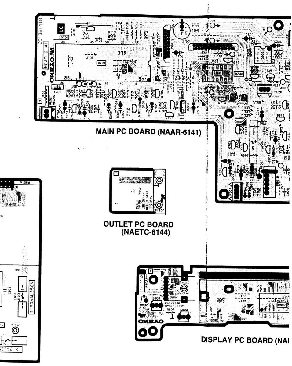
| U1 | 1H376541-1B |
NAAR-6141-1B,Main circuit pc board ass'y
|
| 1H376541-1C |
NAAR-6141-1C,Main circuit pc board ass'y
|
|
| U2 | 1H376542-1B |
NADIS-6142-1B,Display circuit pc board ass'y
|
| 1H376542-1C |
NADIS-6142-1C,Display circuit pc board ass'y
|
|
| U3 | 1H376543-1B |
NAPS-6143-1B,Power supply pc board ass'y
|
| 1H376543-1C |
NAPS-6143-1C,Power supply pc board ass'y
|
|
| U4 | 1H376544-1B |
NAETC-6144-1B,AC outlet pc board ass'y
|
| 1H376544-1C |
NAETC-6144-1C,AC outlet pc board ass'y
|
|
| Z1 | 24650006 | MDM-97XT,MD mechanism ass'y |
- 5 -
EXPLODED VIEW (MD MECHANISM)
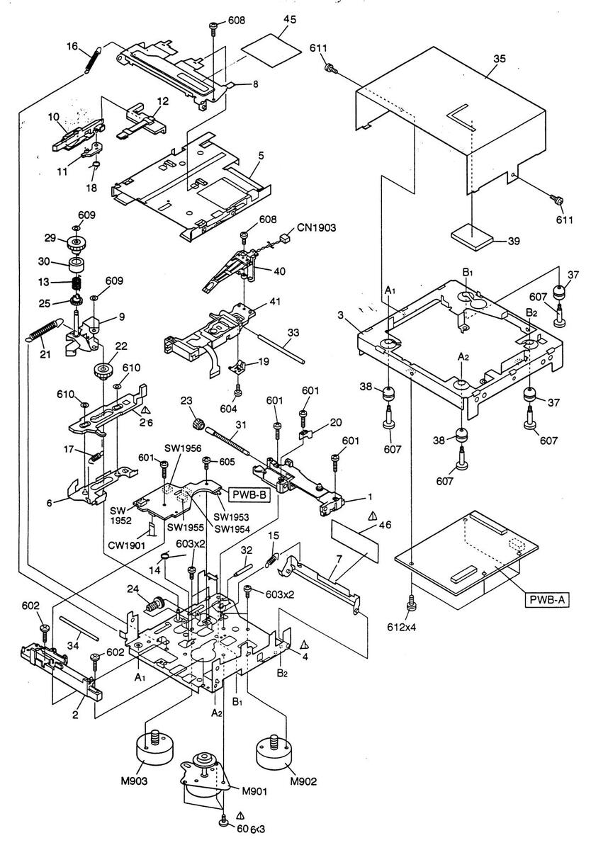
MD MECHANISM PARTS LIST
| REF.NO. | PART NAME | DESCRIPTION | PART NO. | REF.NO. | PART NAME | DESCRIPTION | PART NO. |
|---|---|---|---|---|---|---|---|
| IC1101 | IC | 1R3R55 | 1245730345 | SW1954, SW1955 | Push switch | 1245300026 | |
| IC1201 | IC | LR37648 | 1245730366 | SW1956 | Push switch | 1245300025 | |
| IC1202 | IC | IX2474AF | 1245730207 | 1 | Guide A | 1242000208 | |
| IC1251 | IC | 74ACT02F | 1245730043 | 2 | Guide B | 1242000209 | |
| IC1401 | IC | IX0227AW | 1245730353 | 3 | Base frame | 1242000210 | |
| IC1402 | IC | S29294A | 1245730301 | 4 | Drive chassis | 1242070047 | |
| IC1601 | IC | M56758FP | 1245730354 | 5 | Cartridge holder | 1242140138 | |
| IC1701 | IC | UDA1340 | 1245730357 | 6 | Cam plate lever | 1242480122 | |
| IC1801 | IC | XC62EP32 | 1245730367 | 7 | Shift arm | 1242480123 | |
| IC1802 | IC | NJM431U | 1245730356 | 8 | Holder arm | 1242480124 | |
| IC1906 | IC | TC7ST08F | 1245730152 | 9 | Roller arm lever | 1242480125 | |
| IC1907 | IC | TC9246F | 1245730153 | 10 | Clamper lever | 1242480126 | |
| IC1916 | IC | 74VHC08FT | 1245730368 | 11 | Catcher | 1242480127 | |
| IC1990 | IC | 74AC04FS | 1245730044 | 12 | Slider lever | 1242480128 | |
| Q1251,Q1252 | Transistor | 2SK2909 | 1245760042 | 13 | Roller holder spring | 1242580157 | |
| Q1253,Q1254 | Transistor | 2SK1473 | 1245760016 | 14 | Spindle spring | 1242580159 | |
| Q1401 | Transistor | RN2404 | 1245760032 | 15 | Shift arm spring | 1242580053 | |
| Q1402 | Transistor | RNC1404 | 1305760402 | 16 | Holder arm spring | 1242580054 | |
| Q1403 | Transistor | RN2404 | 1245760032 | 17 | Rack spring | 1242580055 | |
| Q1404 | Transistor | RNC1404 | 1305760402 | 18 | Catcher spring | 1242580094 | |
| Q1451 | Transistor | RNC1407 | 1245760031 | 19 | Plate spring | 1242580160 | |
| Q1601 | Transistor | 2SA1314C | 1245760001 | 20 | Drive shaft spring | 1242580161 | |
| Q1701 | Transistor | 2SC2412KR | 1115760132 | 21 | Roller spring | 1242580093 | |
| Q1801 | Transistor | 2SA1314C | 1245760001 | 22 | Loading gear B | 1242810063 | |
| Q1802,Q1803 | Transistor | RN1406 | 1245760047 | 23 | Drive gear | 1242810064 | |
| Q1804 | Transistor | 2SA1162G | 1305760552 | 24 | Loading gear A | 1242810065 | |
| Q1806 | Transistor | RNC1404 | 1305760402 | 25 | Roller gear | 1242810066 | |
| Q1807 | Transistor | 2SA1314C | 1245760001 | 26 | Rack gear | ····· | 1242810067 |
| Q1820 | Transistor | 2SA1162G | 1305760552 | 29 | Roller holder | 1242860001 | |
| Q1821,Q1822 | Transistor | RNC1407 | 1245760031 | 30 | Transfer roller | 12428/0014 | |
| D1251,D1252 | Diode | SB0209CP | 1245700005 | 31 | Drive shaft | 1242900105 | |
| D1990 | Diode | 1$$372 | 1245700008 | 32 | Loading gear shaft | 1242900108 | |
| L1101 | Coil | 10µH . | 1245850024 | 33 | Slide shaft,opto. pickup | 1242900039 | |
| L1102,L1201 | Coil | 0.47µH | 1245850026 | 34 | Pick-up guide shaft | 1242900040 | |
| L1203 | Coil | 4.7µH | 1245850025 | 35 | Cover | 1242000225 | |
| L1251 | Coil | 47µH | 1245850002 | 37 | Rubber vibration isolator A | 1243260020 | |
| L1601,L1950 | Coil | 1µH | 1246140023 | 38 | Rubber vibration isolator A | 1243260021 | |
| L1701,L1702 | Coil | 10µH | 1245850024 | 39 | Cushion for head | 1243260097 | |
| LR190 | Coil | 4.7μH | 1245850025 | 40 | Head | 1246100008 | |
| XL1201 | Crystal oscillator | 33.8688MHz | 1246160018 | 41 | Optical pickup | 1246170019 | |
| CN1101 | Plug | 23P | 1245100161 | 45 | Protection sheet | ||
| CN1252 | Plug | 2P | 1425100204 | 46 | Protection sheet | 11.7.0.5 | 1240700161 |
| CN1601 | Plug | 5P | 1245100162 | 601 | Screw | Ø1.7X9.5mm | 1249700101 |
| CN1602 | Plug | 2P | 1245100163 | 602 | Screw | Ø1./X/.5mm | 1249700102 |
| CN1603 | Plug | 2P | 1425100236 | 603 | Screw | Ø1./x2mm | 1249/00103 |
| CN1604 | Plug | 2P | 1245100164 | 604 | Screw | Ø1.4x2.2mm | 1249/00011 |
| CN1901 | Plug | 5P | 1245100153 | 605 | Screw | Ø1./X3mm | 1249700001 |
| CN1902 | Plug | 24P | 1245100165 | 606 | Screw | (01.1X2.5mm | 1249/00000 |
| CN1904 | Plug | 4P | 1425100223 | 607 | Screw | Ø 1. /X8.9mm | 1249/00010 |
| CW1901 | Flat cable | 15P | 1245120287 | 608 | Screw | 41 Ex 42 200 E- | 1249700100 |
| CW1903 | Connector | |2P | 1245120288 | 609 | Washer | 1 2 4 2 5 mm | 1249900005 |
| M901 | Spindle motor asser | mbly | 1246300048 | 1010 | $2v/mm | 1189700020 | |
| M902 | Sled motor assembly | / | 1246300049 | 1611 | Speicial Screw | 41 7v2mm | 1249700077 |
| M903 | Loading motor asser |
mbly
T |
1246300050 | 1612 | Screw | 1246840192 | |
| SW1952 | Push switch | 1245300027 | IPWB-A | Main circuit pe board ass | у | 1240040192 | |
| SW1953 | Push switch | 1 | 1305301315 | J |
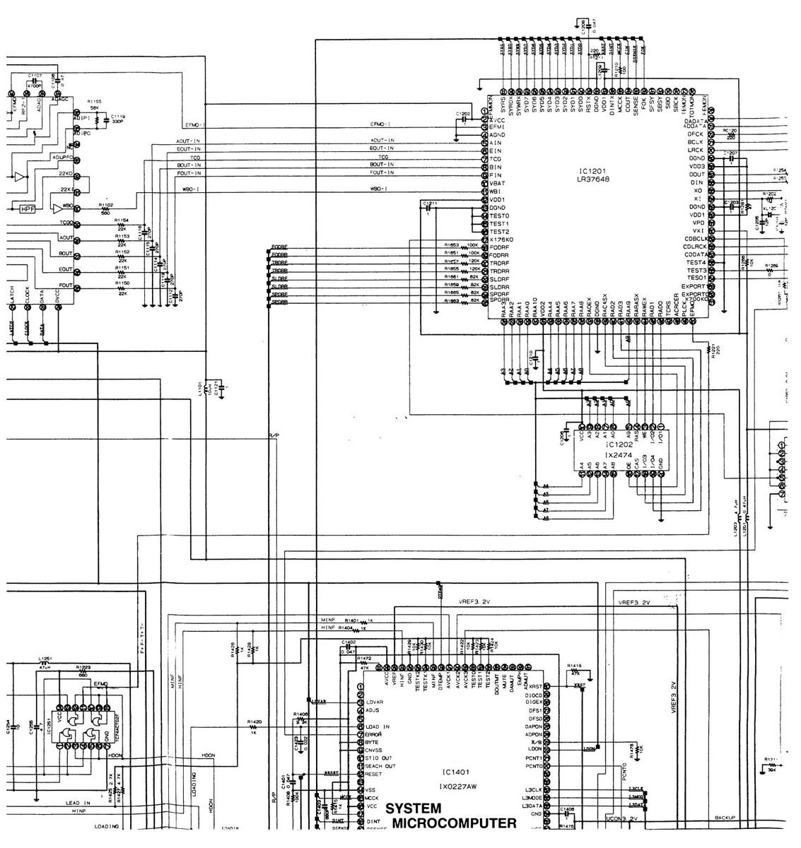
BLOCK DIAGRAM

PARTS LIST
| MAIN CIRCU | IT PC BOARD(NA | AR-6141-1B/1C) | |||
|---|---|---|---|---|---|
| CIRCUIT NO. | PART NU. | DESCRIPTION | |||
| 0101.0102 | 22240191 | NIM4565D-D | C506 | 374721044 | 0.1 μ F±5%, 50V, Plastic |
| O201.O202 | 22240191 | NJM4565D-D | C702 | 354780159 | 1.5 μ F,50V,Elect. |
| 0701 | 22241137 | TMP87CM40AN-4824 | C706,C911 | 354780479 | 4.7 μ F,50V,Elect. |
| Q913 | 22241170T | NJM431L | C707 | 354780109 | 1 μ F,50V,Elect. |
| Q501 | 222740005 | 74HC00P | C901 | 3500181 | 2200 µ F,16V,Elect. |
| Q702 | 222740047TOS | 74HCT04(TC74HCT04AP) | C902 | 354742229 | 2200 μ F,16V,Elect. |
| Q504,Q902 | 222780055JRC | 78M05(NJM78M05FA) | C904,C905 | 374721044 | 0.1 µ F±5%, 50V, Plastic |
| Q901,Q911 | 222780063 | 78L06 | |||
| Q912 | 222790063 | 79L06 | |||
| Photo couplers | |||||
| Q502,Q503 | 24120073 | GP1F32R | |||
| Q502,Q503 | 24120075 | GP1F37R | |||
| Transistors | |||||
| Q105,Q106 | 2211705 or | 2SD655-E or | |||
| 2211706 | 2SD655-F | - | |||
| Q107,Q205 | 2213090 or | DTA114YS or | |||
| 2213590 | RN2207 | ||||
| Q203,Q204 | 221299 or | DTC114TS or | |||
| 2213600 | RN1211 | ||||
| Q703,Q710 | 221281 or | DTC114YS or | |||
| Q711,Q713 | 2213570 | RN1207 | |||
| Q704,Q706 | 2213354 or | 2SA933S-R or | |||
| Q907,Q909 | 2213355 | 2SA933S-S | |||
| Q705,Q709 | 2213090 or | DTA114YS or | |||
| Q712 | 2213590 | RN2207 | |||
| Q707,Q708 | 2211705 or | 2SD655-E or | |||
| Q906 | 2211706 | 2SD655-F | |||
| Q714,Q905 | 221281 or | DTC114YS or | |||
| Q908 | 2213570 | RN1207 | |||
| Q903 | 2202724 or | 2SB1569A-D or | |||
| 2202725 | 2SB1569A-E | ||||
| Q904 | 2213284 or | 2SC1740S-R or | |||
| 2213285 | 2SC1740S-S | ||||
| Diodes | |||||
| D701,D703 | 223163, | 155133, | |||
| D906,D907 | 223205 or | 1SS270A or | |||
| D911 | 223222 | WG713A | |||
| D702,D908 | 224470562 | MTZJ5.6B | |||
| D901-D905 | 22380035 or | GP104003E or | |||
| DOOD | 22380200 | ||||
| D909 | 224472404 | , | |||
| D910 | 224470302 | ; | |||
| Dall | 224410412 | MIZJ4.7B | |||
| 1 701 | 220006T | DI OODNO DEO | |||
| L701 | DLUZKINZ-KUZ | ||||
| V701 | 2010100 | CSTR OOMTW | |||
| X101 | Conscitors | C318.001011 W | |||
| C101 C102 | 27/722215 | 330pF + 10% 50V Plactic | |||
| C101,C102 | 374723313 | 2200 F + 5% 50V Plactic | • | ||
| C107 C108 | 374724714 | 470nF+5% 50V Plastic | |||
| C109 C110 | 354784700 | 47 // F 50V Flect | |||
| C201 C202 | 374721015 | 100pF + 10% 50V Plastic | |||
| C203-C206 | 354741019 | 100 // F 16V Flect | |||
| C505 | 3547922210 | 220 // E 6 3V Elect | |||
| 0000 | JJTILLLIJ | 220 pt 1,0.3 V |
| CIRCUIT NO. | PART NO. | DESCRIPTION |
|---|---|---|
| Capacitors | ||
| C907 | 354762209 | 22 µ F,35V,Elect. |
| C909 | 354781019 . | 100 μ F,50V,Elect. |
| C913,C919 | 354722219 | 220 µ F,6.3V,Elect. |
| C914 | 374721034 | 0.01 µ F±5%, 50V, Plastic |
| C915 | 354742219 | 220 μ F,16V,Elect. |
| C916 | 354721019 | 100 μ F,6.3V,Elect. |
| C917 | 354741029 | 1000 μ F,16V,Elect. |
| C920,C921 | 354744719 | 470 μ F,16V,Elect. |
| C922 | 374723344 | 0.33 μ F±5%, 50V, Plastic |
| • | Resistors | |
| R902 | 453530474 | 4.7Ω±5%,1/2W,Metal |
| R917 | 453532294 | 0.22 Ω ± 5%, 1/2W, Metal |
| R918 | 443528204 | 82Ω±5%,1/2W,Metal oxide |
| Terminals | ||
| P101 | 25045397 | NPJ-4PDWR222 |
| P701 | 25045330 or | NPJ-2PDBL184 or |
| 25045481 | NPJ-2PDBL299 | |
| Plugs | ||
| P501 | 25055442 | NPLG-4P424 |
| P703 | 25055038 | NPLG-2P29 |
| Sockets | ||
| P702 | 25051776 or | NSCT-24P1563 or |
| 25051982 | NSCT-24P1769 | |
| P801B | 25051769 or | NSCT-17P1556 or |
| 25051975 | NSCT-17P1762 | |
| P802A | 2009990467 | NSAS-12P0621 |
| P901B | 25050270 | NSCT-6P98 |
| Holder | ||
| E854 | 27191017A | (FL) |
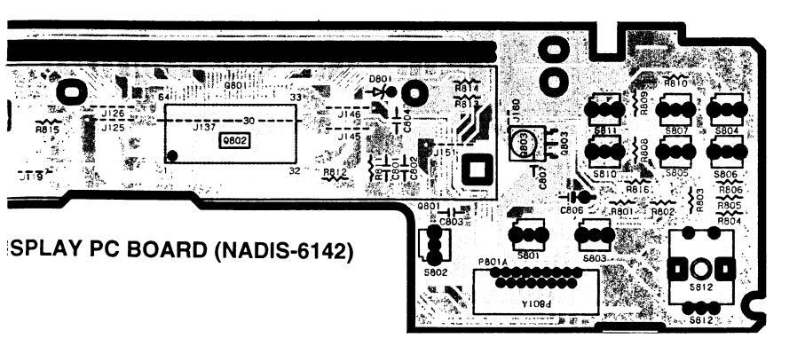
DISPLAY CIRCUIT PC BOARD (NADIS-6142-1B/1C)
| CIRUCIT NO. | PART NO. | DESCRIPTION |
|---|---|---|
| Q801 | 212164 | BJ561GK,FL tube |
| Q802 | 22240685R9 | M66004FP,IC |
| D801 | 224470623T | MTZJ6.2C,Diode |
| D802 | 225338 | SLR-332VR,LED |
| Q803 | 241306 | RPM6938-V4,Remote sensor |
| S801-S811 | 25035652T | NPS-111-S604,Switch |
| P801A | 25051797 | NSCT-17P1584,Socket |
| S812 | 25065507 | EC11B15244,Rotary encoder |
| C806 | 353721019T | 100 µ F,6.3V,Elect. capacitor |
| R817 | 5104362 | N14RGLS10KA15Z, Variable resistor |
POWER SUPPLY CIRCUIT PC BOARD (NAPS-6143-1B/1C)
| CIRCUIT NO. | PART NO. | DESCRIPTION |
|---|---|---|
| L951 | 231252 | NCH-3489,Choke coil |
| E881 | 25050065 |
YSH403T,Fuseholder
|
| P901A | 25051110 | NSCT-6P897,Socket |
| P951 | 25055675 | NPLG-2P631,Plug |
AC OUTLET TERMINAL PC BOARD(NAETC-6144-1B/1C)
| CIRCUIT NO. | PART NO. | DESCRIPTION |
|---|---|---|
| P952 | 25051637 |
NSCT-2P1424,AC outlet
|
| P952 | 25051990 |
NSCT-2P1777,AC outlet
|
MICROPROCESSOR TERMINAL DESCRIPTION Q701:TMP87CM40AN-4824

Q701 TMP87CM040AN-4824
| PIN No. | SYMBOL | DESCRIPTION |
|---|---|---|
| 1 | DIGITAL 172 | Signal output port at digital input |
| 2 | RI IN | RI signal in |
| 3 | RIOUT | RI signal out (Active low) |
| 4 | LINE MUTE ' | LINE MUTE control output port(Active high) |
| 5 | NOT USED | N.C |
| 6 | FILAMENT | Filament control port (Active low) |
| 7 | BACKUP CHECK | Back up cheking |
| 8 | BACKUP POWER | Back up voltage cheking |
| 9 | MECHA POWER | Voltage select for mecha signal |
| 10 | POWER DOWN | Output signal at power failure(active low) |
| 11 | MDRESET | Reset port for mecha micon |
| 12 | MD-ST | communicate a mecha micon |
| 13 | LOAD SWITCH | Signal input port for lording switch |
| 14 | TEST MODE | Test mode detect port(active low) |
| 15 | Dome /Ex-port detect port | |
| 16 | CHECK MODE | Check mode port |
| 17 | ||
| 17 | ANALUG REC MUTE | Analogue recording mute output |
| 10 | ||
| 19 | NOTUSED | |
| 20 | NOTUSED | |
| 21 | NOTUSED | |
| 22 | CS | Chip select port to FL driver(M66004FP) |
| 23 | RES | Reset signal output port to FL driver(M66004FP) active low |
| 24 | POWER OFF | Signal port for power failure |
| 25 | NOT USED | N.C (to GND) |
| 26 | TEST | Test port (connect to GND) |
| 27 | BACKUP INHIBIT | Back up suppression input port |
| 28 | PHOTO MODE | Set-up mode at take a photo |
| 29 | SYSTEM RESET | System reset signal port |
| 30 | XIN | connect to clock(8MHz) |
| 31 | XOUT | connect to clock(8MHz) |
| 32 | Vss | Power supply (to GND) |
| 33 | NOT USED | N.C (to GND) |
| 34 | NOT USED | N.C (to GND) |
| 35 | NOT USED | N.C (to GND) |
| 36 | NOTUSED | N.C (to GND) |
| 37 | NOTUSED | N.C (to GND) |
| 38 | NOTUSED | N.C (to GND) |
| 39 | NOTUSED | N.C. (to GND) |
| 40 | STAND-BY I FD | Output control port for stand-by LED |
| 41 | NOTUSED | |
| 42 | Signal output (voltage control.) for DSCK KDATA | |
| 42 | Signal output (voltage control ) for book, kb/tr/ | |
| 43 | Serial communication port to mecha micon(output terminal) | |
| 45 | Serial communication port to mecha micon(input terminal) | |
| 15 | ||
| 40 | ||
| 4/ | ||
| 48 | Serial data port to FL driver(M66004FP) | |
| 49 | NOTUSED | |
| 50 | NOT USED | N.C (to GND) |
| 51 | NOT USED | N.C (to GND) |
| 52 | NOT USED | N.C (to GND) |
| 53 | NOT USED | N.C (to GND) |
| 54 | VASS | Reference voltage port for A/D transfer(to GND) |
| 55 | VAREF | Reference voltage port for A/D transfer(to +5V) |
| 56 | NOT USED | N.C (to GND) |
| 57 | NOT USED | N.C (to GND) |
| 58 | BACKUP | A/D input for backup voltage |
| 59 | A/D KEY(1) | A/D key input port |
| 60 | A/D KEY(2) | A/D key input port |
| 61 | R.ENCODER(B) | Pluse in port for rotaly-encoder |
| 62 | R.ENCODER(A) | Pluse in port for rotaly-encoder |
| 63 | REMOCON | Input signal for remote control |
| 64 | VDD | Power supply (to + 5 V) |
UDA1340 A/D,D/A CONVERTER
| PIN No. | SYMBOL | DESCRIPTION |
|---|---|---|
| 1 | VSSA | Analogue power supply port for ADC (Ground) |
| 2 | VDDA | Analogue power supply port for ADC |
| 3 | VINL | Input port for ADC (Lch) |
| 4 | VREFA | Reference voltage for ADC |
| 5 | VINR | Input port for ADC (Rch) |
| 6 | VADCN | Reference voltage for ADC(N-port) |
| 7 | VADCP | Reference voltage for ADC(P-port) |
| 8 | TEST 1 | Test1 control port |
| 9 | OVERFL | Output port flag for over load |
| 10 | VDDD | Power supply for digital |
| 11 | VSSD | Power supply for digital(Ground) |
| 12 | SYSCLK | System clock(256,384 or 512fs) |
| 13 | L3CLOCK | L3 clock port(data in) |
| 14 | L3MODE | L3 mode port(data in) |
| 15 | L3DATA | L3 data port(data in) |
| 16 | BCK | Bit clock port |
| 17 | WS | Word select input |
| 18 | DATAO | Data output port |
| 19 | DATAI | Data input port |
| 20 | TEST3 | Test port for data output |
| 21 | TEST2 | Test control port 2 |
| 22 | AVSS | Power supply for analogue DAC(Ground) |
| 23 | AVDD | Power supply for analogue DAC |
| 24 | VOUTR | Output port for DAC (Rch) |
| 25 | VDDO | Power supply for OP Amp |
| 26 | VOUTL | Output port for DAC (Lch) |
| 27 | VSSO | Power supply for OP Amp(Ground) |
| 28 | VREFD | Reference voltage port for DAC |

Q802:M66004FP (FL TUBE,DRIVER)

-14-

- 15 -
IC1101:IR3R55 (RF SIGNAL PROCESSOR)
| PIN No. | SYMBOL | DESCRIPTION |
|---|---|---|
| 1 | RF1 | RF signal input port1(to pick up) |
| 2 | RF2 | RF signal input port2(to pick up) |
| 3 | RF3 | RF signal input port3(to pick up) |
| 4 | RF4 | RF signal input port4(to pick up) |
| 5 | REF1 | Reference voltage (input) |
| 6 | REF0 | Reference voltage (output) |
| 7 °° | RFADD | Add output ports of RF1 to RF4 |
| 8 | TCGI | Track cross detect input port |
| 9 | AIN | Focus-servo signal amplifire |
| 10 | BIN | Focus-servo signal amplifire |
| 11 | EIN | Tracking-servo signal amplifire |
| 12 | FIN | Tracking-servo signal amplifire |
| 13 | BIAS | Bias signal input port |
| 14 | AVCC | Power supply for analogue part |
| 15* | VSTBY | Logic-signal output(STBY signal) |
| 16* | XDISC | Logic-signal output(DISC signal) |
| 17* | XSGAIN | Logic-signal output(SGAIN signal) |
| 18 | AGND | GND port (analogue part) |
| 19 | DGND | GND port (digital part) |
| 20 | DTEMP | Detect a chip-emperature |
| 21 | LATCH | Latch signal input |
| 22 | CLOCK | Clock signal input |
| 23 | DATA | Serial data input |
| 24 | DVCC | Power supply for digital ports |
| 25 | FOUT | Output signal port for tracking servo |
| 26 | EOUT | Output signal port for tracking servo |
| 27 | BOUT | Output signal port for focus servo |
| 28 | AOUT | Output signal port for focus servo |
| 29 | TCGO | Track cross detect output port |
| 30 | WBO | Comparetor output port (ADIP signal) |
| 31 | 22KI | Comparetor input port (ADIP signal) |
| 32 | 22KO | HPF signal output port (ADIP signal) |
| 33 | ADLPFO | LPF signal output port (ADIP signal) |
| 34* | NC | NC |
| 35 | ADIPO | Pre-amp output port (ADIP signal) |
| 36 | ADIPI | AGC-amp output port (ADIP signal) |
| 37 | ADAGC | Conect a across-capacitor for AGC (ADIP signal) |
| 38 | ADAGI | AGC-amp input port (ADIP signal) |
| 39 | RF2-1 | Difference signal of RF1 to RF2 |
| 40 | EFMO | Pre-amp output port (RF signal) |
| 41* | EFMI | AGC-amp output port (RF signal) |
| 42 | AVCC | Power supply of analogue part |
| 43 | AGND | GND port of analogue part |
| 44 | EFMAGC | AGC capacitor connect port (EFM signal) |
| 45 | EFMAGI | AGC-amp input port (EFM signal) |
| 46* | ATTR | Output signal adjust port (47 and 48pin) |
| 47 | GOUT | RF1+RF2+RF3+RF4 signals output |
| 48 | POUT | RF1 to RF4 output |
*This mark terminals is open port.
IC1601:5 CHANNEL ACTUATOR DRIVER IC
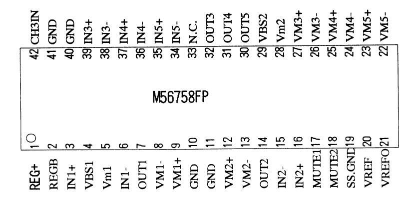
| PIN No. | SYMBOL | DESCRIPTION | PIN N |
|---|---|---|---|
| 1 | REG+ | Voltage setting port for regulator | 42 |
| 2 | REGB | Connect base position for regulator | 41 |
| 3 | IN1+ | Non-inverted input port of E1-amp. | 40 |
| 4 | VBS1 | Power supply for boost-trap | 39 |
| 5 | Vm1 | Power supply of moter | 38 |
| 6 | IN1- | Inverted input port of E1-amp. | 37 |
| 7 | OUT1 | Output port of E1-amp. | 36 |
| 8 | VM1- | Inverted output port of CH1 | 35 |
| 9 | VM1+ | Non-inverted output port of CH1 | 34 |
| 10 | GND | Ground(moter) | 33 |
| 11 | GND | Ground(moter) | 32 |
| 12 | VM2+ | Non-inverted output port of CH2 | 31 |
| 13 | VM2- | Inverted output port of CH2 | 30 |
| 14 | OUT2 | Output port of E2-amp. | 29 |
| 15 | IN2- | Inverted input port of E2-amp. | 28 |
| 16 | IN2+ | Non-inverted input port of E2-amp. | 27 |
| 17 | MUTE1 | Mute ports of CH1 to CH4 | 26 |
| 18 | MUTE2 | Mute port of CH5 | 25 |
| 19 | SS.GND | Ground(signal) | 24 |
| 20 | VREF | Input port of voltage reference | 23 |
| 21 | VREFO | Output port of voltage reference | 22 |
| PIN No. | SYMBOL | DESCRIPTION |
|---|---|---|
| 42 | CH3IN | Non-inverted input port of CH3 |
| 41 | OUT3 | Output port of E3-amp. |
| 40 | IN3- | Inverted input port of E3-amp. |
| 39 | VBS2 | Power supply for boost-trap |
| 38 | Vm2 | Power supply of moter |
| 37 | IN3+ | Non-inverted input port of CH3 |
| 36 | N.C. | N.C |
| 35 | VM3- | Inverted output port of CH3 |
| 34 | VM3+ | Non-inverted output port of CH3 |
| 33 | GND | Ground(moter) |
| 32 | GND | Ground(moter) |
| 31 | VM4+ | Non-inverted output port of CH4 |
| 30 | VM4- | Inverted output port of CH4 |
| 29 | VM5+ | Non-inverted output port of CH5 |
| 28 | VM5- | Inverted output port of CH5 |
| 27 | OUT5 | Output port of E5-amp. |
| 26 | IN5- | Inverted input port of E5-amp. |
| 25 | IN5+ | Non-inverted input port of E5-amp. |
| 24 | IN4+ | Non-inverted input port of E4-amp. |
| 23 | IN4- | Inverted input port of E4-amp. |
| 22 | OUT4 | Output port of E4-amp. |
MD-105
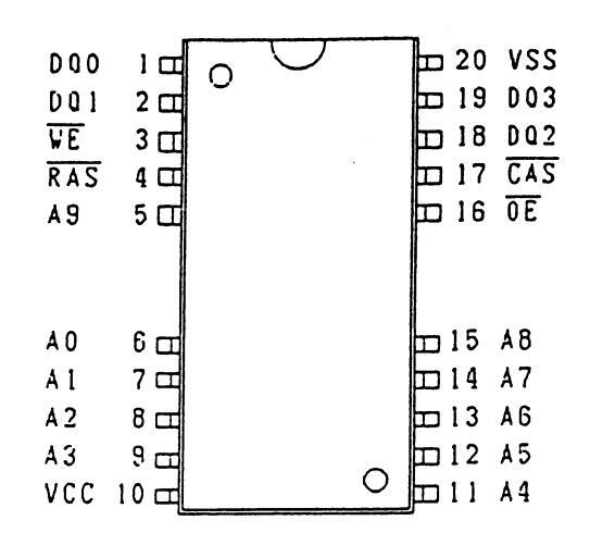
IC1402:S29294A (EEP-ROM) PROGRAMMABLE ROM


| PIN | PIN No. | DESCRIPTION |
|---|---|---|
| CS | 3 | Chip select(Input) |
| SK | 4 | Serial clock(input) |
| DI | 5 | Serial data(input) |
| DATA | 6 | Serial data(output) |
| GND | 7 | Ground |
| PROTECT | 8 |
Protect controlled of
memory(input) |
| Connect GND or open :Effective protect | ||
| NC | 1 | To Vcc : Ineffective protect |
| No. | Upen | |
| VCC | 2 | Supply voltage |
IC1201:LR37648 (ENCODER/DECODER)

IC1201:LR37648 (ENCODER/DECODER)
| PIN No. | PIN NAME | I/0 | DESCRIPTION |
|---|---|---|---|
| 1 | EFMMON | 0 | EFM monitor |
| 2 | AVCC | • - | Power supply for analogue use |
| 3 | EFMI | Ι | EFM signal from RF amplifier |
| 4 | AGND | - | GND (analogue) |
| 5 | AIN | Ι | Focus error signal A |
| 6 | EIN | Ι | Tracking error signal E |
| 7 | TCG | Ι | Tracking loss signal |
| 8 | BIN | Ι | Focus error signal B |
| 9 ` | FIN | Ι | Tracking error signal F |
| 10* | VBAT | Ι | Detect signal for power supply(servo regulator) |
| 11 | WBI | Ι | ADIP wobble signal |
| 12 | VDDI | - | Power supply for digital use |
| 13 | DGND | - | Ground for digital use |
| 14/15 | TEST0, TEST1 | Ι | Test port(normally,connect to GND) |
| 16 | TEST2 | Ι | Test port(normally,connect to GND) |
| 17 | X176KO | 0 | Clock output(f=176.4kHz) |
| 18 | FODRF | 0 | Focus servo forward output. PWM |
| 19 | FODRR | 0 | Focus servo reverse output. PWM |
| 20 | TRDRF | 0 | Tracking servo forward output.PWM |
| 21 | TRDRR | 0 | Tracking servo reverse output.PWM |
| 22 | SLDRF | 0 | Slide servo forward output.PWM |
| 23 | SLDRR | 0 | Slide servo reverse output.PWM |
| 24 | SPDRF | 0 | Spindle servo reverse output or switching motor's rotation |
| 25 | SPDRR | 0 | Spindle servo forward output or switching motor's rotation |
| 26 | RAA3 | 0 | Address to D-RAM(ADR3) |
| 27 | RAA2 | 0 | Address to D-RAM(ADR2) |
| 28 | RAA1 | 0 | Address to D-RAM(ADR1) |
| 29 | RAA0 | 0 | Address to D-RAM(ADR0) LSB |
| 30* | RAA 10 | 0 | Address to D-RAM(ADR10) MSB |
| 31 | VDD2 | - | Power supply for interface (D-RAM) |
| 32 | RAA4 | 0 | Address output to external D-RAM ADR4 |
| 33 | RAA5 | 0 | Address output to external D-RAM ADR5 |
| 34 | RAA6 | 0 | Address output to external D-RAM ADR6 |
| 35 | RAA7 | 0 | Address output to external D-RAM ADR7 |
| 36 | RAA8 | 0 | Address output to external D-RAM ADR8 |
| 37 | RAOEX | 0 | Data output signal(enable) to external D-RAM |
| 38 | DGND | - | Digital section GND |
| 39 | RACASX | 0 | Column address signal output to external D-RAM |
| 40 | RAD2 | I/0 | Data I/O port of external D-RAM D2 |
| 41 | RAD3 | I/0 | Data I/O port of external D-RAM D3(MSB) |
| 42 | RAD9 | 0 | Data I/O port to D-RAM ADR9 |
| 43 | RARASX | 0 | Low address strobe signal to external D-RAM |
| 44 | RAWEX | 0 | Data write enable signal to external D-RAM |
| 45 | RAD1 | I/0 | Data I/o port with external D-RAM D1 |
| 46 | RAD0 | I/0 | Data I/O port with external D-RAM D1 |
| 47* | TCRS | 0 | Truck cross signal |
| 48* | ACRCER | 0 | CRC error Flag monitor output for ADIP |
| 49* | PLCK | 0 | EFM PLL clock signal output at playback |
| 50 | EFM0 | 0 | EFM signal output at recording, CIF monitor output at playback |
| note : * marks is open port. | |||
| PIN No. | PIN NAME | I/0 | DESCRIPTION |
|---|---|---|---|
| 51* | X700KO | 0 | Clock output.f=705.6kHz |
| 52* | EXPORT0 | 0 | Micon.expander output "0"port |
| 53* | EXPORT1 | 0 | Micon.expander output "1"port |
| 54 | TESO1 | 0 | When change the PLLLR, MICON.expander output port 2 |
| 55 | TEST3 | I/0 | When change the PLLOSC, MICON.expander output port 3 |
| 56 | TEST4 | I/0 | When change the EXTCLK, MICON.expander output port 4 |
| 57 | CDDATA | I/0 | CD data input port for fast dubbing. |
| 58 | CDLRCK | I/0 | CDLR clock input for fast dubbing. |
| 59 | CDBCLK | I/0 | CD bit clock input for fast dubbing. |
| 60 | VXI | Ι | PLL clock input for variable-pitch. |
| 61* | VPO | 0 | PLL phase deference output for variable-pitch. |
| 62 | VDD1 | - | Power supply for digital |
| 63 | DGND | - | Ground(digital) |
| 64 | XI | Ι | Oscillation circuit (input) 33.8088MHZ |
| 65 | X 0 | 0 | Oscillation circuit (output) 53.80881412 |
| 66 | DIN | Ι | Digital input signal |
| 67 | DOUT | 0 | Digital output signal |
| 68 | VDD3 | - | Power supply for internal PLL |
| 69 | DGND | - | Ground(digital) |
| 70 | LRCK | 0 | Lch/Rch select output port for music data |
| 71 | BCLK | 0 | Shift clock for music uata |
| 72 | DFCK | 0 | Clock for AD/DA converter (digital filter) 2001 5 |
| 73 | ADDATA | 1 | Voice input data |
| 74 | DADATA | 0 |
Voice output data
Monitor output for focus error signal |
| 75* | FEMON | 0 | Monitor output for focus offor signal |
| 76* | TOTMON | 0 | Monitor output port for tracking error signal |
| 77* | TEMON | U | Reading clock sub-code |
| 78* | SBCK | 1 | Serial sub DIN code |
| 79 * | SBO | 0 | Synchronized block sub-code signal |
| 80* | SBSY | 0 | Synchronized frame sub-code signal |
| 81* | SFSY | 0 | Focus detect signal Focus good is "0" code |
| 82 | FUN | 0 | Servo condition detect signal |
| 03 | COUT |
ů
0 |
Truck cross output signal |
|
04
85 |
MCCK | 0 | Clock output signal for micon. |
|
86
86 |
DINTX | 0 | Interruption output port to system interface |
| 87 | VDD1 | - | Digital power supply |
| 88 | DGND | - | Ground(digital) |
| 89 | RSTX | Ι | Chip reset input(L = reset) |
| 90 | SYD0 | I/( | ) Data buss port of interface (LSB) |
| 91 to 96 | SYD1 to SYD6 | I/( | ) Data buss port of interface |
| 97 | SYD7 | I/( | ) Data buss port of interface (MSB) |
| 98 | SYWRX | Ι | Pulse input port of writing resister |
| 99 | SYRDX | Ι | Pulse input port of reading resister |
| 100 | SYRS | Ι | Resister input select port of interface |
note: * marks is open port.
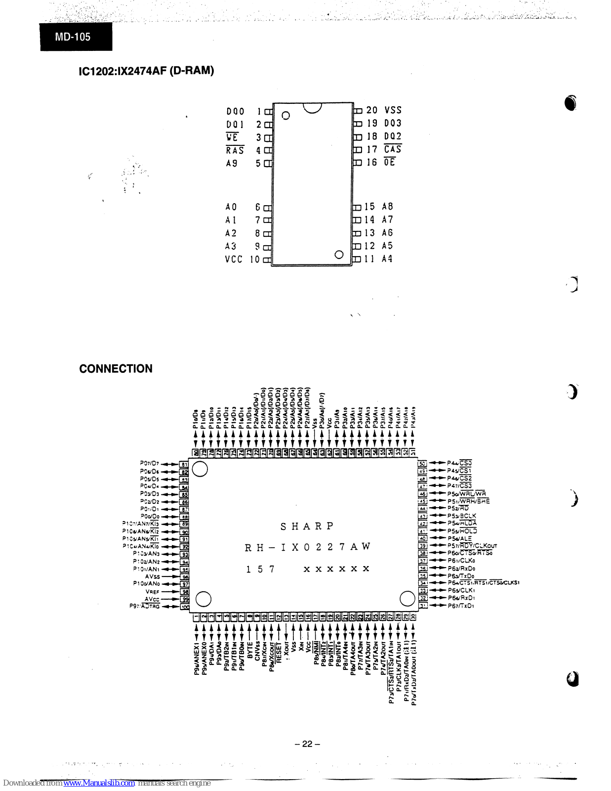
IC1202:IX2474AF (D-RAM)
CONNECTION
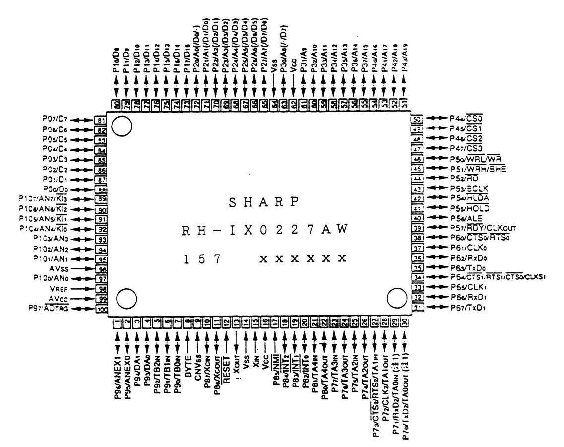
IC1401:IX0227AW (SYSTEM MICROCOMPUTER)
| PIN No. | PIN NAME | I/O | DESCRIPTION |
|---|---|---|---|
| 1* | P96/ANEX1 | 0 | I/O port P96 |
| 2* | P95/ANEX0 | 0 | I/O port P95 |
| 3 | P94/DA1 | о | Adjust output of lessor power LDJS |
| 4* | P93/DA0 | о | ADJS for auto adjusting step check |
| 5* | P92/TB2IN | о | I/O port P92 |
| 6 | P91/TB1IN | I | LD SW CK input |
|
e
7 |
P90/TB0IN | I | ERR input |
|
,
8 |
BYTE | I | GND |
| 9 | CNVss | I | GND |
| 10* | P87/XCIN | 0 | ST-ID output |
| 11* | P86/Xout | 0 | MD search output |
| 12 | RESET | I | Reset input |
| 13* | Xout | - | Clock output |
| 14 | Vss | - | GND |
| 15 | Xin | I | Crystal (8.4672MHz) |
| 16 | Vcc | - | +3.15V |
| 17 | P85/NMI | I | I/O port P85 |
| 18 | P84/INT2 | Ι | D INT |
| 19 | P83/INT1 | I | D SENSE(Servo-sens. input from MD-LSI) |
| 20 | P82/INTO | I | ST-ID (MD on) |
| 21 | P81/TA4IN | I | CD serch input |
| 22 | P80/TA4out | 0 | MD RSW input |
| 23* | P77/TA3in | I | Frequency select for swiching power supply |
| 24 | P76/TA3out | 0 | Variable pitch output port |
| 25 | P75/TA2IN | I | Power failure detect port P-DOWN |
| 26 | P74/TA2out | о | On/off output for magunetic-head current HDON |
| 27 | P73/TA1IN | о | Loading motor output and control lsignal output LD+ |
| 28 | P72/TA1out | 0 | Loading motor output and control lsignal output LD- |
| 29 | P71/TA0in | Ι | Truck counts signal input CIN |
| 30 | P70/TA 0out | I | Inner switch detect input INN SW |
| 31 | P67/TXD1 | 0 | R-DATA |
| 32 | P66/RXD1 | 0 | R-LATCH |
| 33 | P65/CLK1 | 0 | R-CLK |
| 24 | P64/CTS1/RTS1/ | 0 | Communication's possible to system |
| 34 | CTS0/CLKS1 | U | Communication's possible to system |
| 35 | P63/TXD0 | 0 | MD data output MD DATA |
| 36 | P62/RXD0 | I | System control data output K DATA |
| 37 | P61/CLK0 | I | System communication clock input |
| 38 | P60/CTS0/CLKour | Ι | D RAM(4M/16M) input select |
| 39 | P57/RDY/CLKout | 0 | REC/PLAY select output port R/P |
| 40 | P56/ALE | Monitor input for focus servo condition FOK | |
| 41* | P55/HOLD | 0 | I/O port P55 |
| 42 | P54/HLDA | 0 | S2 output |
| 43 | P53/BCLK | 0 | S1 output |
| 44 | P52/RD | 0 | Resister select signal (MD-LSI) output SYRS |
| 45 | P51/WRH/BHE | 0 | Lead signal output (MD-LSI) SYRD |
| 46 | P50/WRL/WR | 0 | Write signal output (MD-LSI) SYWR |
| 47 | P47/CS3 | I/C | Data bus 7 SYS D7 |
| 48 | P46/CS2 | I/C | Data bus 6 SYS D6 |
| 49 | P45/CS1 | I/C | Data bus 5 SYS D5 |
| 50 | P44/CS0 | I/C | D Data bus 4 SYS D4 |
| note : * mark is open port | |||
| PIN No. | PIN NAME | I/O | DESCRIPTION | ||
|---|---|---|---|---|---|
| 51 | P43/A19 | I/O | Data bus 3 SYS D3 | ||
| 52 | P42/A18 | I/O | Data bus 2 SYS D2 | ||
| 53 | P41/A17 | I/O | Data bus 1 SYS D1 | ||
| 54 | P40/A16 | I/O | Data bus 0 SYS D0 | ||
| 55* | P37/A15 | ' 0 | I/O port P37 | ||
| 56* | P36/A14 | 0 | I/O port P36 | ||
| 57* | P35/A13 | 0 | I/O port P35 | ||
| 58 | P34/A12 | 0 | EEPROM protect mode cancel EEPRO | ||
| 59 | P33/A11 | О | EEPROM chip selector output EEPD | ||
| 60 | P32/A10 | I/O | EEPROM serial data output | ||
| 61 | P31/A9 | о | EEPROM serial clock output | ||
| 62 ` | Vcc | I | +3.15V | ||
| 63* | P30/A8 | ο | I/O port P30 | ||
| 64 | Vss | - | Ground | ||
| 65 | P77/A7 | 0 | Soft serial communication LSB fast and 2-mode output L3 DATA | ||
| 05 | 12//// | Ŭ | Soft serial communication , LOB Tasi, and 2 mode output LO DATAT | ||
| 66 | P26/A6 | 0 | Soft serial communication ,LSB fast, and 2-mode output L3 MODE | ||
| 67 | P25/A5 | ο | Soft serial communication ,LSB fast, and 2-mode output L3 CLK | ||
| 68* | P24/A4 | 0 | I/O port P24 | ||
| 69* | P23/A3 | о | I/O port P23 | ||
| 70 | P22/A2 | о | PCNT0 output | ||
| 71* | P21/A1 | ο | I/O port P21 | ||
| 72 | P20/A 0 | ο | LDON output | ||
| 73 | P17/D15 | ο | ANLPTR output | ||
| 74* | P16/D14 | о | ADPON output (for CK) | ||
| 75* | P15/D13 | о | DAPON output (for CK) | ||
| 76* | P14/D12 | о | |||
| 77* | P13/D11 | ο | DSS1 output | ||
| 78* | P12/D10 | о | DIG EX output (for CK) | ||
| 79* | P11/D9 | ο | DIG CD output (for CK) | ||
| 80 | P10/D8 | 0 | System reset output XRST | ||
| 81* | P07/D7 | 0 | ADMUTE output | ||
| 82* | P06/D6 | 0 | EMPHA output | ||
| 83* | P05/D5 | õ | DAMUTE output | ||
| 84* | P04/D4 | 0 | |||
| 85* | P03/D3 | õ | |||
| 86 | P02/D2 | T | TEST2 (select special model 2) | ||
| 87 | P01/D1 | T | TEST1 (select special model1) | ||
| 88 | P00/D0 | T | TESTI (select special model1) | ||
| 89 | P107/AN7/K13 | Ť | AVCK3 (special monitor mode input) | ||
| 90 | P106/AN/K12 | T | Monitor(3.1V) input for AD/DA sections) AVCK2 | ||
| 91 | P105/AN5/K11 | T | Monitor(5.1 ) input for DOUT section AVCK1 | ||
| 92 | P104/AN4/K10 | Ţ | Detect input for temperature DTEMP | ||
| 93 | P103/AN3 | T | Becainput detect MINE | ||
| 94 | P102/AN2 |
r
T |
Test key innut1 TEST K1 | ||
| 95 | P101/AN1 | T | Test key input TEST K2 | ||
| 96 | AVss | - | Ground | ||
| 97 | P100/AN0 |
-
T |
Mecha and head position detect nort HINE | ||
| 98 | VREF | 1 | |||
| 99 | AVcc | - | 13.15 V | ||
| 100 | P97/ADTE |
-
T |
I/O nort P97 | ||
| note : * mark is one | n port | ||||
| . r | |||||
MD-105 mu-100 Check before & after replacing the mechanism parts and how to replace it
1 Type Number of Mechanism- MDM-970K
2 Optical Pickup replacement
2-1 Conditions to replace ontical nickup
Conditions to replace optical pickup Before replacing the ontical nickup, be sure to confirm below listed points and perform the replacement only when abnormal symptom is found. Ask detail analysis with the Disc attached if the cause is uncertain for the problem such as skipping sound. In that case, carefully examine if the Dies is not wrong
- 1). If error signal at focus or tracking is found abnormal.
- 2). If focus and tracking actuator does not work. (Tracking actuator can be observed by Circuit Tester at #8 and #9 pin of IC M56758FP.)
- 3). Motion of actuator is not smooth enough. (Focus actuator can be confirmed during Search operation by using transparent Disc. Tracking can not be checked with this method.)
- 4). Use Pre-mastered Disc and check if jitters is more than 9.5nsec with KIKUSUI 6135 or if jitters is more than 24nsec with I FADER I. IM-1851
-
5). Use Recordable Disc and check if jitters is more than 11.0nsec with KIKUSUI 6135 or if jitters is more than 28nsec with LEADER LJM-1851.
- * If jitters can not be measured at MDM-970K test point, observe the RF wave form by using
- 6). If C1 error rate is more than 40 by Pre-mastered Disc.
- 7). If C1 error rate is more than 60 by Recordable Disc.
- 8). If value of Lasor Power meter is too low at play mode and recording mode.
- 9). Grating is out of spec, even if the position of spindle motor is aligned.
2-2. How to check
- 1) Check by using separate document "MD-105 MD mechanism measurement methods" for above item 4) to 9) of 2-1.
-
2-3 Replacement process of optical pickup
- 1) Disconnect 4 sockets (white x2 red and blue colored) and CN1601 (FFC 5 leads ) on the PCB.
- 2). Unscrew the 4 screws which fix the PCB. Raise the PCB from the right side of front view. leaving the left side (pick up FFC side) in place. Unlock the CN1101 socket and pull out the FFC.
- 3) Open the roller-arm lever toward the arrow shown in illustration and push back the clamper lever.
- 4). Add 5 volts to the blue color socket of loading motor, bush the rack gear toward the arrow and move the cam plate lever until it clatters. (Refer to Fig. 2-1)
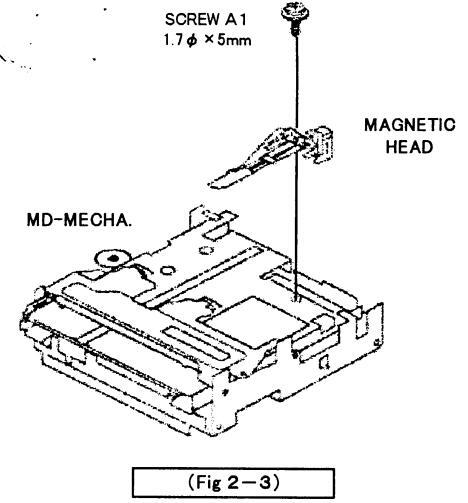
- 5) Add 2 volts (Circuit Tester can be used) to the red color socket of pick motor. move the pick to the outermost position and remove the magnetic head. (M1.7 x5 screw)
- 6). Unscrew the screw (M1.7x5) that fix the spring on arm holder and remove the spring at the left side.
- 7). Move the holder arm to the left side and remove it together with cartridge holder.
- 8). Unscrew the 3 screws (M1.7x10) on the molded parts that
fix the shaft of the pick up andremove the pick If possible, do not remove the mechanism switch PCB by unscrewing the screws(front M1.7x10, back M1.7x3), since it will result difficult work
to build the PCB with all of the 3 switches at ON position.
- 9). Install a new pick and confirm the motion. Then, remove the metal fitting from the back side ofdefective pick and attach it on the new pick by using M1.4x2 screw
- 10). Attach the holder arm and cartridge holder which were removed at above item 7 and also attachthe screws and spring which were removed at above item 6.
- 11). Insert and lock the pick up FFC to the socket CN1101, and fix the PCB by using screws
- 12). Insert the 2 sockets of the motor (except the blue color) and insert the FFC at CN1601.
- 13). Attach the magnetic head and insert the socket to the PCB.
- 14). Add 5 volts at the blue color socket to move back the mechanism to the EJECT position.

2-4. Check after the replacement
- After the replacement, confirm the following points are within the specifications.
- 1). Error rate measured by Pre-mastered Disc must be within the specification.
- 2). Error rate measured by Recordable Disc must be within the specification 3) Error rate at self recording/playback must be within the specification.
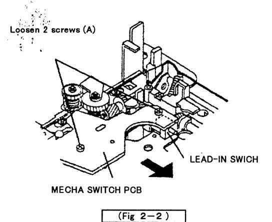
- 4). Measurements for the location of lead-in switch must be within the specification. If not, adjust it referring to Fig. 2-2
- 5). Confirm the Grating is within the specification.

-
3-1. Replacement process
- 1). Pull out the red color socket( CN1604) of slide motor and head(CN1252), add 5 volts at the socket(CN1604) to move the pick up to the outermost position.
- 2). Pull out the socket of magnetic head, unscrew and replace the head (refer to Fig. 2-3)
- 3). Insert the sockets of magnetic head and slide motor.
3–2. Check after the replacement
Make recording and measure the error rate by using the recorded disc. Error rate must be within the specification
(Note). Refer to separate document (MD-105 MD mechanism measurements methods) for the measurement methods and the specifications
-
4. Replace the spindle motor When a motor get old, metalic dust will adhere around the brush and it will decrease the impedance by causing a shor circuit on the coil. This will result an insufficient capability of the driving circuitry andunstable rotating To detect this, connect a digital multi meter (Circuit Tester is not good) to the moter and rotate the moter may cause skipping etc. slowly by hand. If the resistance decreases at paticular point, the motor is defective. Defective motormay cause skipping sound, etc..
-
4-1. Procedure to replace the spindle motor
- 1). Disconnect four sockets (white x2, red and blue) and CN1601 (FFC 5 leads) on the PCB.
- 2). Unscrew the four screws which fix the PCB. Raise the PCB from the right side of front view, leaving the left side (pick up FFC side) in place. Unlock the CN1101 socket and pull out the FFC
- 3). Unscrew the three screws that fix the spindle motor and replace the motor. Fasten the screw temporarily for alignment.
-
4-2. Alignment after the replacement
- 1). Use an extension JIG and connect it as shown in Fig. 4-2.
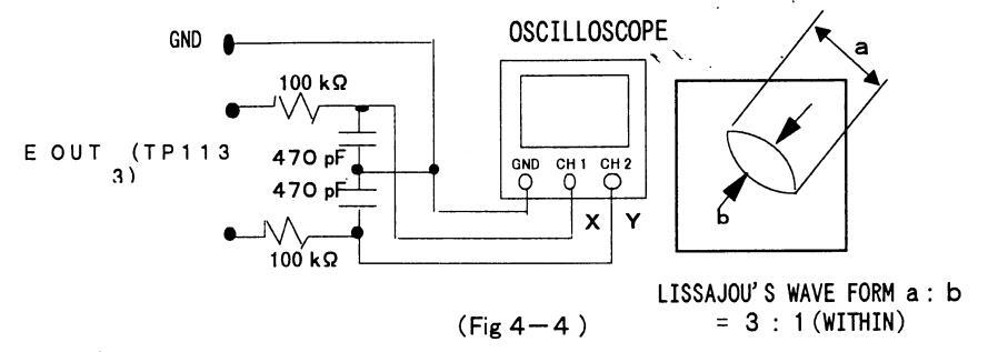
- 2). Connect an oscilloscope to the test points of the PCB as shown in Fig. 4-3. (Refer to Fig. 4-4 for the wirings.)
- 3). Adjust the position of spindle motor while observing the lissajous' figure,by using a screw driverput into the hole for adjustment. (Refer to Fig. 4-4)
-
4-1. Procedure to replace the spindle motor


6P-2P EXTENSION CONNECTOR

MD-105
MD mechanism measurement items and measurement methods
- 1. Type number of Mechanism: MDM-970K
- 2. Error rate
-
2-1. Pre-mastered Disc
- 1). Connect the right side of R720 (5.6k ohms, at Q701 side) and the chassis. Plug in the AC plug to the wall outlet.
- 2). Push the ENTER key of remote control (RC-301MD or RC-339MD) to enter the TEST mode. Confirm the display shows "tsm***** and then it changes to "EJECT"
- 3). Insert the Pre-mastered Disc (TCD-381) and confirm the display shows "AUT YOBI".
-
4). Turn the AMCS knob counterclockwise by one click and confirm the display shows "TEST PLAY". 5). Push INPUT key and confirm the display shows "ADRES 0050"
- ADRES shows the location of the pick and lager number means outer location of the disc. Turning the AMCS knob counterclockwise will change the ADRES number to measure the error rate of desired point.
- 0050 is the inner, 03C0 is the middle, 0700 is the outer and 08A0 is the outermost position.
-
6). Push PLAY/PAUSE key. The display shows "s****c****" and error rate measurement will start. Four digit numerals following the "s" show the subcode address and four digit numerals following the "c" show C1 error rate.
- Ascertain the quality of MD mechanism and Disc by the value of error rate. Error rate is defined to be less than 220 in RAINBOW BOOK, although there is no error rate specified for the
- Pre-mastered Disc. Onkyo has an internal specification for the Pre-mastered Disc error rate,
-
as a criterion to ascertain the MD mechanism. Pre-mastered Disc error rate =< 40
Just after starting playback, error rate is displayed as if it is big. However, this is no problem.
2-2. Recordable Disc
- 1). Push EJECT key and exchange the disc to Recordable Disc (issued by MD Proj., MD01).
- 2). Confirm the display indicates "AUT YOBI". Turn the AMCS knob counterclockwise and confirm the display shows "TEST PLAY"
- 3). Push INPUT key and confirm the display shows "ADRES 0050"
- 4). Push PLAY/PAUSE key and confirm the display shows "a****c****". Error rate measurement will start
Four digit numerals following the "a" show the address and four digit numerals following the "c" show C1 error rate.
-
Similary, Onkyo has an internal specification as shown below.
- Recordable Disc error rate =< 60
2-3. Self recording/playback disc
- 1). Push EJECT key and exchange the disc to the self recording/playback disc. (If it is not available, cancel the test mode, make self recording/playback disc and reenter the test mode.)
- 2). Confirm the display indicates "AUT YOBI". Turn the AMCS knob counterclockwise and confirm the display shows "TEST PLAY"
- 3). Push INPUT key and confirm the display shows "ADRES 0050".
- 4). Push PLAY/PAUSE key and confirm the display shows "a****c****". Error rate measurement will start.
Four digit numerals following the "s" show the address and four digit numerals following the "c" show C1 error rate
Onkyo has an internal specification as shown below.
Self recording/playback disc error rate =< 60
* In case of self recording/playback disc, rewriting might have been done many times and the song with larger track number is not necessarily located at outer side. Be careful for this when measure the error rate by designating the address.
3. Jitter
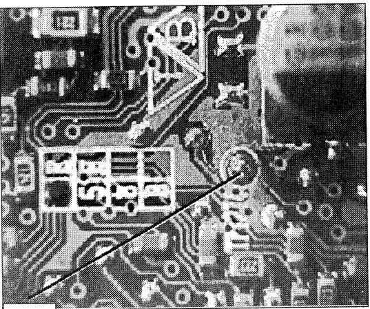
3–1. Pre-mastered Disc
- 1). Solder a lead wire at the RF-TP point shown in the Fig. 3-1 PCB picture and connect it to Jittermeter.
- Measure the jitter while playing at the same test modes as error rate measurements.
-
3) Onkyo internal specifications
- KIKUSUI 6135: Less than 9.5nsec LEADER LJM-1851: Less than 24.0nsec * Jitter might not be able to measure for MDM-970K mechanism when jitter meter is connected at the test point, due to the unstable RF signal. In that case, observe the wave form by oscilloscope to ascertain the guality.
3–2. Recordable Disc and Self recording/playback disc
1) Use same procedure as Pre-mastered Disc for measurements.
2). Onkyo internal specifications
KIKUSUI 6135: Less than 11.0nsec
LEADER LJM-1851: Less than 28.0nsec
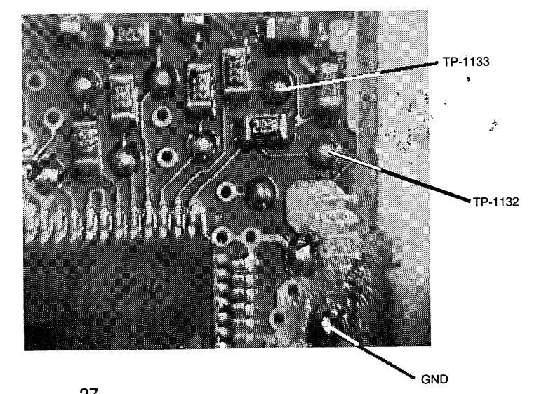
(Note): Refer Fig. 6-1 for GND connection.
-
4. Measurement for Read-in position
- 1). Connect the right side of R720 (5.6k ohms, at Q701 side) and the chassis. Plug in the AC plug to the wall outlet.
- 2). Push the ENTER key of remote control (RC-301MD or RC-339MD) to enter the TEST mode. Confirm the display shows "tsm******* and then it changes to "EJECT".
- Inset the disc and confirm the display shows "AUT YOBI". Push the STOP key and the display will change to "tsm*****".
- 4). Push DISPLAY key and confirm the display shows "INNER".
-
5). Push PLAY/PAUSE key and confirm the display shows "s****c****.
- Four digit numerals following the "s" show the position of read-in switch. The specification is in between FF85 and FFD2.
-
5. Lasor power measurement
- 1). Connect the right side of R720 (5.6k ohms, at Q701 side) and the chassis. Plug in the AC plug to the wall outlet.
- 2). Push the ENTER key of remote control (RC-301MD or RC-339MD) to enter the TEST mode. Confirm the display shows "tsm****e**" and then it changes to "EJECT".
- 3). Put the optical sensor of lasor power meter (LEADER 8001 or 8010) to the objective lens of pick up.
- 4). Each time to push INPUT key will change the display to "xpw", "rpw" and "ppw". Measure the power for each position.
Do not keep the "rpw" and "xpw" conditions for long. Especially, measure the power for "xpw" within 15 seconds.
Reference value: "xpw" 6.8 mW +/- 5% "rpw" 5.2 mW +/- 5% "Ppw" 0.62mW +/- 5%
-
6. Grating check
- Solder lead wires at the points shown in the Fig 6-1 PCB picture and connect them to oscilloscopeas shown in Fig 6-2. Set the oscilloscope as shown in Fig 6-2. Set the oscilloscope at AC input, 20mV/DIV range.
- Connect the right side of R720 (5.6k ohms, at Q701 side) and the chassis. Plug in the AC plugto the wall outlet.
- 3). Push the ENTER key of remote control (RC-301MD or RC-339MD) to enter the TEST mode. Confirm the display shows "tsm******" and then it changes to "EJECT".
- 4). Insert the Pre-mastered Disc and confirm the display shows "AUT YOBI". Push STOP key and the display will change to "tsm****e**".
- Turn the AMCS knob clockwise by two clicks and confirm the display shows "AUTO AJST". Push PLAY/PAUSE key.
- 6). Confirm the display changes to "PEG:", "HAG:" and then "COMPLETE". Wave form of the Gratingis shown in the oscilloscope.

Pick-up grating measurement
7. Cancel the test mode
Unplug the AC plug from wall outlet to cancel the test mode.
Message List
The following table explain the various messages that appear in the display.
| Message | meaning | |||
|---|---|---|---|---|
| Blank Disc | A new recordable MD or a recordable MD without disc or track names is inserted. | |||
| Cannot Copy | An attempt was made to make a second copy from a digitally dubbed MD. | |||
| Cannot Edit | An attempt was made to edit the disc during MEMORY or RANDOM play, or in recording standby mode, | |||
| or an attempt to edit a premastered disc was made. | ||||
| Cannot Rec | An attempt was made to record onto a premastered (read-only) disc. | |||
| D. In Unlock | The digital equipment (CD player, DAT, etc) has not been connected properly. Otherwise, the connected | |||
| digital equipment is not operating properly. | ||||
| Disc Error | The disc is abnormal (scratched or missing a TOC). | |||
| Disc Full | The disc is full. | |||
| Impossible | The disc could not be edited. | |||
| Mecha Error | An error occurred in the unit's internal mechanism. | |||
| Memory Full | An attempt was made to record a 26th track. | |||
| Name Full | The titling capacity of the disc has reached its limit. | |||
| No Change | The naming attempt failed. | |||
| No Disc | There is no disc in the unit. | |||
| No Track | The inserted disc has a disc title but no tracks. | |||
| Not Audio | An attempt was made to play a non-audio disc. | |||
| Over | In pause mode (when playing is paused) : the Fast Forward button ( ) was pressed to the end of the disc. | |||
| Protected | The inserted disc is record-protected. | |||
| Retry Error | The recording attempt failed due to a consecutive disturbance or scratches on the MD. | |||
| Temp Over | An abnormally high temperature is detected in the unit's internal mechanism. | |||
| TOC Error | The reading of the TOC failed. | |||
| TOC Writing | The unit is writing the recorded or edited contents to the MD. | |||
| U-TOC Error | The writing of the recorded or edited contents failed. | |||
MD MECHANISM SECTION
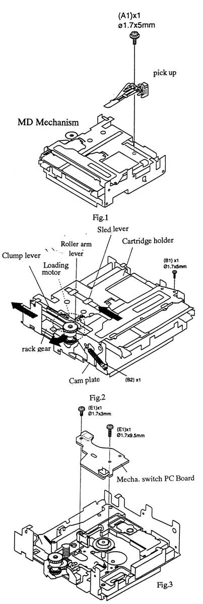
• Remove the optical head
(refer to Fig.1)
1. Screw (A1) take off.
• Cartridge holder take off (refer to Fig.2)
• Mecha switch PC Board take off. (refer to Fig.3)
MD MECHANISM DISASSEMBLY
note: Procedure to reset the Mechanism
Be sure to reset the mechanism, when you exchanged it. Follow next procedure for the reset.
1) Remove the top cover of the unit.
Temporarily connect either of RESET MECHA terminals (2p terminal) on the main PCB (NAAR-6141) to the chassis (GND) by using a lead wire with clips at each side.
- Plug in the AC plug to the wall outlet, keeping above lead ) wire connected
- 4) Disconnect above lead wire.
- 5) Turn on the unit
• Sled motor/Loading motor take off (refer to Fig.4)

• Spindle motor take off (refer to Fig.5)
• Optical pick up take off (refer to Fig.6)

Insert the Pre-mastered disc,. Setting is AUTO Mode (TEST MODE) and then auto adjust. (Indicate on display "COMPLETE") 3)3 screws of spindle motor few loosen ,then readjusting screws while look at the oscilloscope.
- 35 -


NAAR-614
- 36 –
– B
--- : PLAY BACK SIGNAL
RECORDING SIGNAL

| 1 L | |||
|---|---|---|---|
| i r | I G | ||
|
|
ENCODER/DECODER


.
* ....................................
MD-105 MD-105
PC BOARD (BOTTOM VIEW)
POWER SUPPLY PC BOARD (NAPS-6143)


| REF.NO. | PART NO. | DESCRIPTION |
|---|---|---|
| 1 | 29053219 | Carton box |
| 2 | 29095799 | Sheet |
| 3 | 29100156 | Poly bag |
| 4 | 29110071 | PP tape |
| 5 | 261504 | Paper tape |
| 6 | 29362226 | Label EAN |
| 7 | 2010098A or | Audio cord |
| 7 | 2010326 | Audio cord |
| 7 | 2010200 | Cord RI |
| 7 | 24140339 | RC-339MD,Remote control |
| 7 | 3010054 | UM-3,Battery |
| 8 | 29100180 | 240*250,Poly bag |
| 8 | 29355267 | Instruction sheet |
| 8 | 29342496 | Instruction manual |
| 8 | 29342533 | Instruction manual T |
| 8 | 29342519 |
Instruction manual FG
|
| 8 | 2050039 | NCS-1P104,Opto. cord |
MD-105
(a) A set of a set
ONKYO CORPORATION
International Sales Div.: 31 Sankyo-bild. 3-8-5, Asakusabashi, Taito-ku, TOKYO 111, JAPAN TEL : 03-5820-5865 FAX : 03-5820-5869
ONKYO U.S.A. CORPORATION 200 Williams Drive, Ramsey, N.J. 07446, U.S.A. TEL : 201-825-7950 FAX : 201-825-8150
ONKYO EUROPE ELECTRONICS GmbH Industriestrasse 18-20, 82110 Germering, GERMANY TEL : 089 84 93 20 FAX : 089 84 93 226
ONKYO FRANCE Immeuble Le Diamant, Domaine Technologique de Saclay, 4 Rue Rene Razel, 91892 SACLAY, FRANCE TEL : (1) 69 33 1400 FAX : (1) 69 41 35 84


 Loading...