

Page 1
SERVICE MANUAL
MINIDISC RECORDER
MODEL MD-101A
MD-101A
Ref. No. 3703
112001
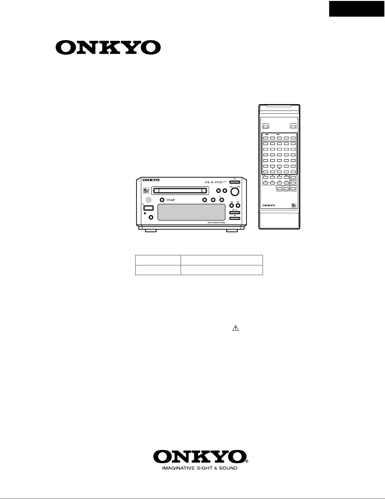
MINIDISC RECORDER
DISC LOADIING MECHANISM
INPUT
STANDBY / ON
STANDBY
DISPLAY
MDT
MGT, MGR
MULTI JOG
EDIT / NO YES
CD
DUBBING
REC
PUSH TO ENTER
MD
REC MODE
Silver models
120V AC, 60Hz
220-230V AC, 50/60Hz
STANDBY/ON
PLAY MODE
CONTINUE
RANDOM MEMORY
ABCDE
1
2345
FGHI J
6117
KLMNO
12
PQRST
16
17
UVWXY
21
22
Z
REPEAT A-B A.SPACE M.SCAN
>
25
/
?
REC
REMOTE CONTROLLER RC-
-
101
A
8
13
18
23
!
SCROLL DISPLAY
475
MD
EJECT
9
10
14
15
19
20
24
25
.,
(
CLEAR
ENTER
NAME
)
RC-475MD
SAFETY-RELATED COMPONENT
WARNING!!
COMPONENTS IDENTIFIED BY MARK ON THE
SCHEMATIC DIAGRAM AND IN THE PARTS LIST ARE
CRITICAL FOR RISK OF FIRE AND ELECTRIC SHOCK.
REPLACE THESE COMPONENTS WITH ONKYO
PARTS WHOSE PART NUMBERS APPEAR AS SHOWN
IN THIS MANUAL.
MAKE LEAKAGE-CURRENT OR RESISTANCE
MEASUREMENTS TO DETERMINE THAT EXPOSED
PARTS ARE ACCEPTABLY INSULATED FROM THE
SUPPLY CIRCUIT BEFORE RETURNING THE
APPLIANCE TO THE CUSTOMER.
Page 2

SPECIFICATIONS
MD-101A
System
MiniDisc digital audio system
Recording system
Magnetic field modulation overwrite system
Signal read out system
Optical non-contact
Recording time
Stereo: Max. 80 min.
(when using MDW-80)
Mono : Max. 160 min.
(when using MDW-80)
Number of revolutions
About 400 - 900 rpm (constant linear velocity)
Error correction system
Advanced Cross Interleave Reed-solomon code
Sampling frequency
44.1 kHz
Number of channels
2 (stereo)
Frequency response
10 Hz - 20 kHz ( 0.5 dB)
Signal to noise ratio
100 dB or more when playing
Output level
2.0 volts r.m.s.
Power supply rating
AC 230-240 V, 50/60 Hz
AC 120 V, 60 Hz
Power consumption
13 watts (AC 230-240 V, 50/60 Hz)
15 watts (AC 120 V, 60 Hz)
Dimensions (W H D)
155 76 288.5 mm
Weight
2.3 kg
Specifications and features are subject to
change without notice.
Page 3

DISPLAY MESSAGES
MD-101A
Message
Auto Space
Blank Disc
Cannot Copy
Cannot Edit
Cannot Rec
CD Dub Fail
Complete
D. In Unlock
Disc Error
Disc Full
Full
Impossible
Mecha Error
Memory Full
Music Scan
Name Full
No Change
No Disc
No Track
Over
Protected
Retry Error
Signal Wait
Synchro Rec
TOC Reading
TOC Writing
TOC Error
Meaning
This message appears during the track intervals when A. Space is turned on.
A new recordable MD or a recordable MD without disc or track names is inserted.
An attempt was made to record copyright-protected material. An attempt was made to make a
second copy from a digitally dubbed MD
An attempt was made to edit the disc during MEMORY or RANDOM play or in recording standby
mode, or an attempt to edit a premastered disc was made.
An attempt was made to record onto a premastered (read-only) disc.
The CD dubbing operation could not be enabled. Check the connections. (An RI cable or audio
pin cable is not connected. "Digital In 1" is not selected as an input source, or the amplifier or CD
player is not turned on.)
Editing is complete.
The digital equipment (CD player, DAT, etc.) has not been connected properly. Otherwise, the
connected digital equipment is not operating properly.
The disc is abnormal (scratched or missing a TOC).
The disc is full.
An attempt was made to enter a character that exceeds the maximum character capacity.
The disc could not be edited.
An error occurred in the unit fs internal mechanism.
An attempt was made to record a 26th track.
Music Scan has started.
Number of characters has reached the limit for input to one MD.
The naming attempt failed.
There is no disc in the unit.
The inserted disc has a disc title but no tracks.
In pause mode (when playing is paused), the >>(Fast Forward) button was pressed to the end
of the disc.
The inserted disc is record-protected.
The recording attempt failed due to a consecutive disturbance or scratches on the MD.
The unit has entered Signal Wait mode.
Synchro recording has started.
The unit is reading the TOC from the MD.
The unit is writing the recorded or edited contents to the MD.
The writing of the recorded or edited contents failed. Something is wrong with the TOC.
Page 4
SERVICE PROCEDURES
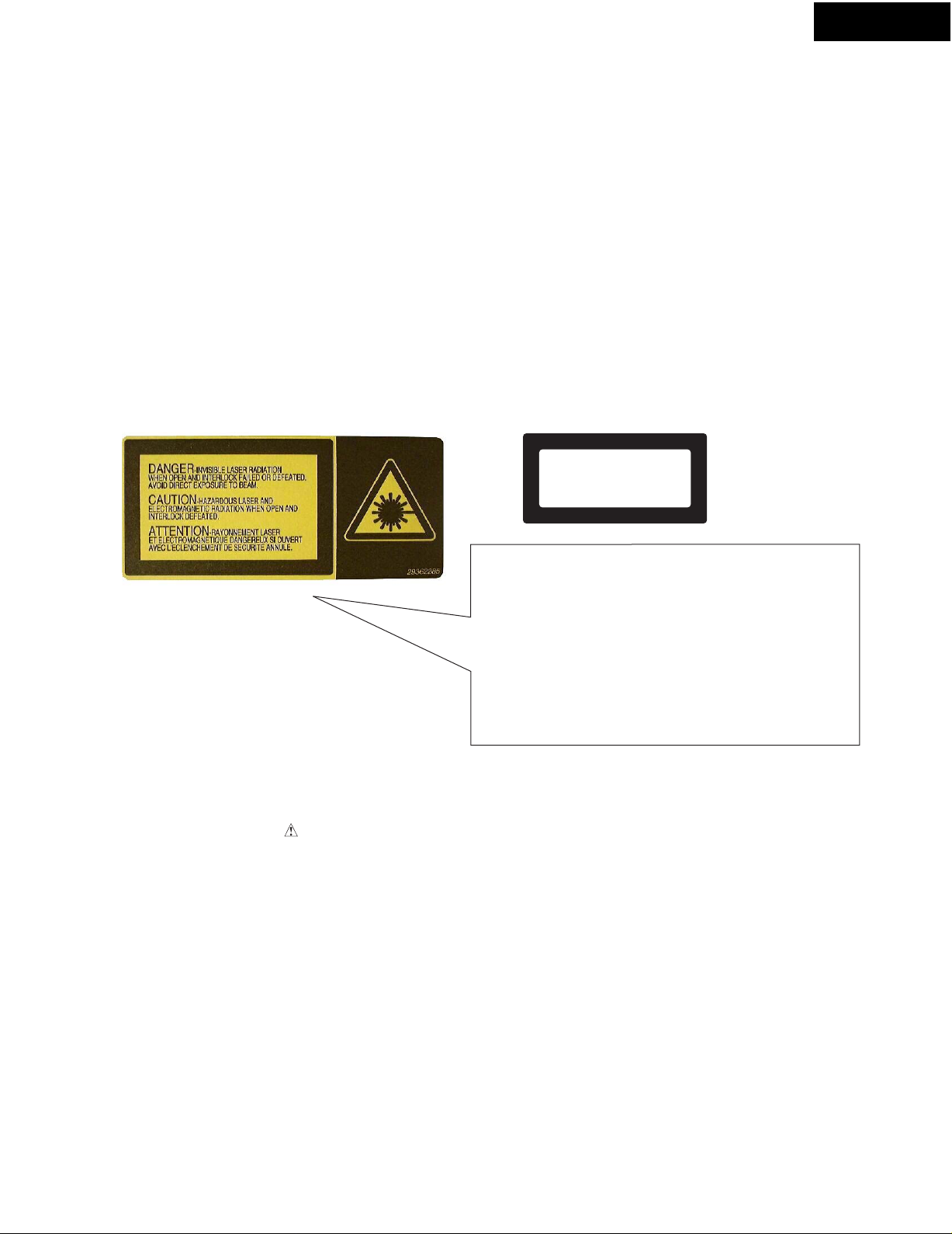
PROTECTION OF EYES FROM LASER BEAM DURING SERVICING
This set employs a laser. Therefore, be sure to follow
carefully the instructions below when servicing.
WARNING!!
SERVICE WARNING : DO NOT APPROACH THE
LASER EXIT WITH THE EYE TOO CLOSELY.
IN CASE IT IS NECESSARY TO CONFIRM LASER
BEAM EMISSION, BE SURE TO OBSERVE FROM
A DISTANCE OF MORE THAN 30cm FROM THE
SURFACE OF THE OBJECTIVE LENS ON THE
OPTICAL PICKUP BLOCK.
LASER W ARNING LABEL
The labels shown below are affixed.
1. Warning label
Laser Diode Properties
Material:
Wavelength:
Emission Duration:
Laser output:
2. Class 1 label
"CLASS 1 LASER
PRODUCT"
GaAS/GaAlAs
780 nm
Continuous
MAX. 7 mW
MD-101A
LUOKAN 1
LASERLAITE
KLASS 1
LASER APPARAT
SERVICE PROCEDURE
1. Replacing the fuses
REF. NO.
F901
[NOTE ]
<GT> : Asian model
<GR> : Chinese model
PART NO.
252074
2. To initialize the unit
(1) Connect the power supply cord in the wall socket.
(2) Press the STANDBY/ON button to turn the power source on.
(2) While hold down the YES button, press the DISPLAY button.
(4) Press the STANDBY/ON button.
(5) Disconnect the power supply cord.
DESCRIPTION
2A-SE-EAK, Fuse <GT, GR>
DANGER:
INVISIBLE LASER RADIATION WHEN OPEN AND
INTERLOCK FAILED OR DEFEATED. AVOID DIRECT
EXPOSURE TO BEAM.
CAUTION:
HAZARDOUS LASER AND ELECTROMAGNETIC
RADIATION WHEN OPEN AND INTERLOCK DEFEATED.
ATTENTION:
RAYONNEMENT LASER ET ELECTROMAGNETIQUE
DANGEREUX SI OUVERT AVEC L'ECLENCHEMENT
DE SECURITE ANNULE.
3. How to reset the unit compulsorily
Used when it becomes impossible to eject a disk.
Continues pressing the
STOP
button more than for 5 seconds.
Page 5
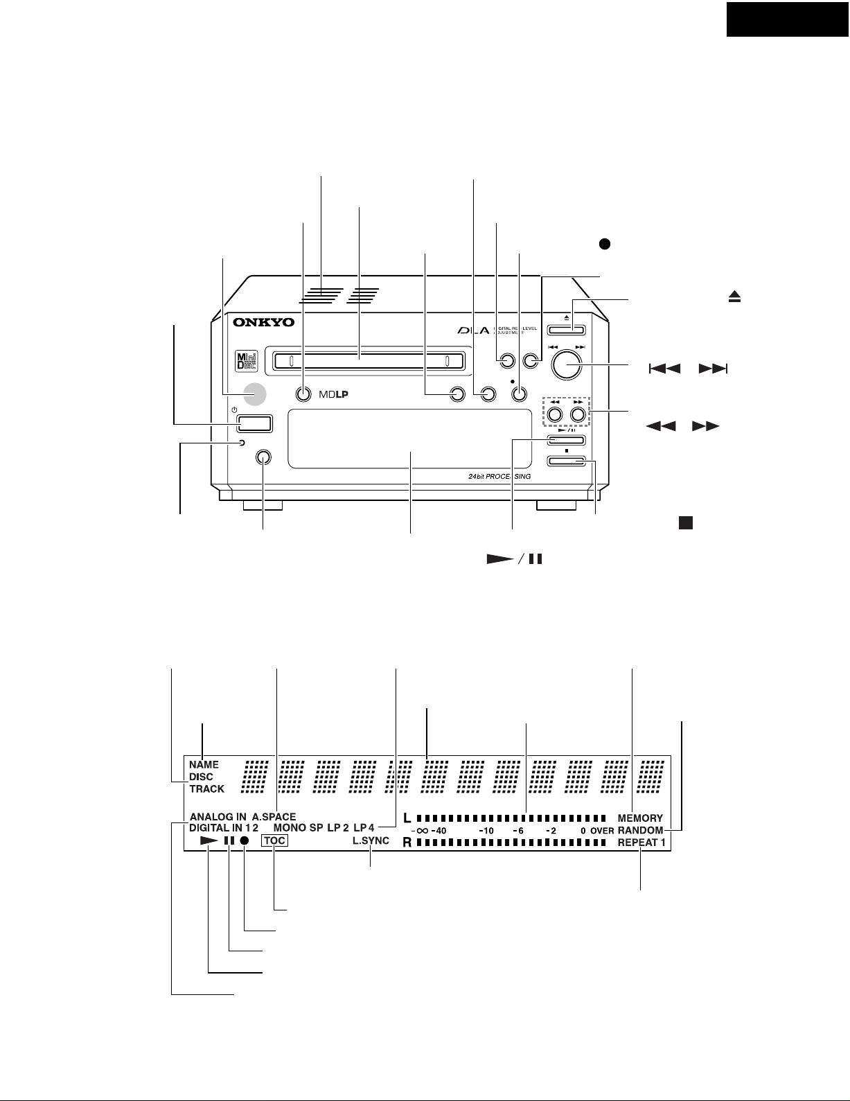
P ANEL VIEWS-1
FRONT PANEL
Ventilation
holes
MD-101A
CD DUBBING
button
Remote control
sensor
STANDBY/ON
button
STANDBY
indicator
INPUT
button
DISPLAY
button
Disc slot
REC MODE
button
Display
EDIT/NO
button
REC button
Play/Pause button
( )
( REC)
YES button
Eject button
MULTI JOG knob
( )
FF/FR button
( )
Stop button
( )
( )
DISPLAY
DISC/TRACK
indicator
NAME
indicator
Input setting indicator
A.SPACE
indicator
TOC indicator
REC indicator
PAUSE indicator
PLAY indicator
REC MODE
indicator
Time/Title
display
L.SYNC indicator
Peak level
meter
MEMORY
indicator
RANDOM
indicator
REPEAT/REPEAT1
indicator
Page 6
P ANEL VIEWS-2
CONNECTING TO THE OTHER COMPONENTS
This unit uses heat-sensitive parts. Do not place this unit on the Amplifier or Receiver.
Connections
MINIDISC RECORDER
REMOTE
CONTROL
cable
MODEL NO. MD-101A
DIGITAL INPUT
12
2
OUT
CD player,
DAT deck, etc.
AC OUTLET
AC 220
-230 V
50 / 60 Hz
UNSWITCHED
100 W MAX.
3
Audio
connection
cable
LR LR
1
OUT IN
ANALOG
INPUT OUTPUT
L
R
Optical fiber
cable
Amplifier
MD-101A
To wall outlet
Connecting to the Amplifier
1
Connect the MD-101A to the MD (or TAPE)
jacks of your amplifier.
2
Connecting to the Digital Input
Terminals (DIGITAL INPUT 1, 2)
You can perform digital recording on the MD101A if a CD (Compact Disc) player or DAT
(Digital Audio Tape) deck equipped with a digital
(OPTICAL) output terminal is available. For digital
recording, you need to connect the equipment
to either DIGITAL INPUT 1 or 2 terminal using
the supplied optical cable.
These terminals can also
be used for connecting an
amplifier that is equipped
with a digital output
terminal.
Note
If you use DIGITAL INPUT 2 to connect an
amplifier, you will be unable to utilize the full
capabilities of the MD-101A.
If you attempt to perform digital recording using
a digital input terminal that is not connected,
"D.In Unlock " will appear.
Terminal protection caps are attached to the
DIGITAL INPUT terminals. Remove the cap for the
terminal you wish to use when connecting the
MD-101A to digital equipment. Replace the caps
if you are not using the DIGITAL INPUT terminals.
3
Connection to AC outlet
(UNSWITCHED)
The power cord of another unit can be connected
to this outlet.
Note
The shape, number, and total capacity of the AC
outlets may differ depending on the area in which
the unit is purchased.
230-240 V, 50/60 Hz model: Capacity is 100 W in
total.
120 V, 60 Hz model: Capacity is 120 W in total.
230-240V, 50/60Hz models
Capacity is
100 watts.
120V, 60Hz models
Capacity is
120 watts.
Page 7
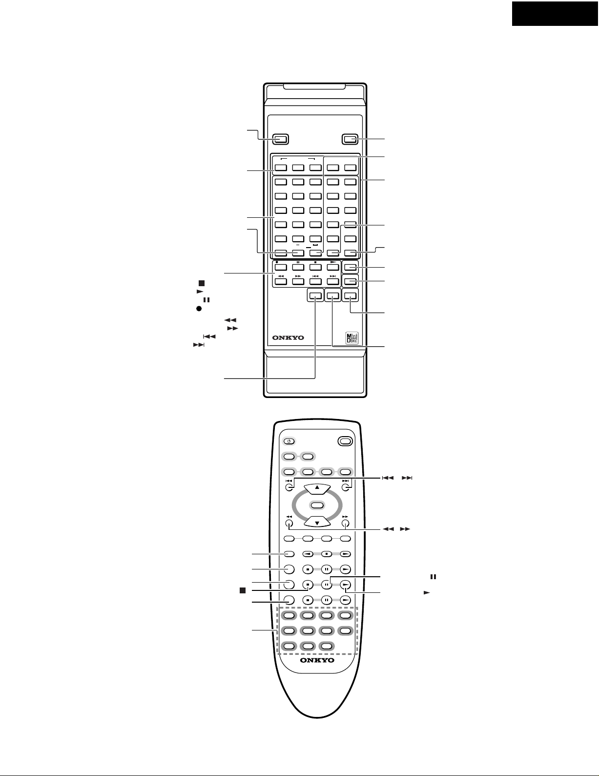
REMOTE CONTROLLER
RC-475MD (supplied)
MD-101A
STANDBY/ON button
PLAY MODE buttons
CONTINUE buttons
RANDOM button
MEMORY button
Number buttons
REPEAT button
MD operation buttons
Stop button ( )
Play button (
Pause button (
Rec button (
)
)
REC)
Fast reverse button (
Fast forward button (
Down button ( )
Up button (
)
SCROLL button
STANDBY/ON
EJECT
EJECT button
PLAY MODE
CONTINUE
RANDOM MEMORY
ABCDE
1
2345
FGHI J
6117
KLMNO
PQRST
16
UVWXY
21
Z
>
25
/
REC
8
9
13
12
17
22
REPEAT A-B A.SPACE M.SCAN
?
14
18
19
23
24
!
SCROLL DISPLAY
.,
(
CLEAR
ENTER
NAME
10
15
20
25
)
)
A-B repeat button
Uppercase and
lower case letters,
symbols, and
numbers (1~10)
buttons
A.SPACE button
M.SCAN button
CLEAR button
ENTER button
NAME button
)
REMOTE CONTROLLER RC-
475
MD
DISPLAY button
RC-466S
(supplied with the R-801A)
Mode button (MODE)
Repeat button (REPEAT)
Clear button (CLEAR)
Stop button ( )
Scroll button (SCROLL)
Number buttons
STANDBY/ ON
CDR/PC
CD/ DVD
TAPE REW TAPE FF
SLEEP TIMER ENTER
MODE
REPEAT
CLEAR
SCROLL
1
5
9
ACOUSTIC
PRESENCE
TAPE
MD FM AM
U
L
O
V
UP
MUTING
DOWN
CLOCK
CD/DVD
CDR/PC
2
6
10/0
REMOTE CONTROLLER
INPUT SELECTOR
M
E
TAPE
MD
3
7
--/---
-
466S
RC
4
8
, button
, button
Pause button ( )
Play button ( )
Page 8
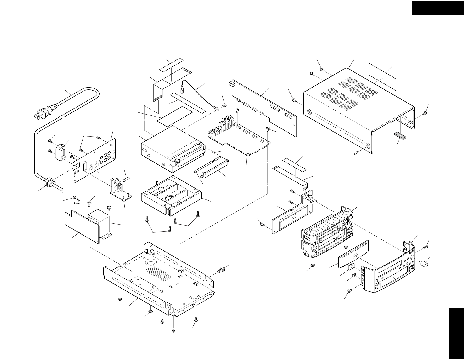
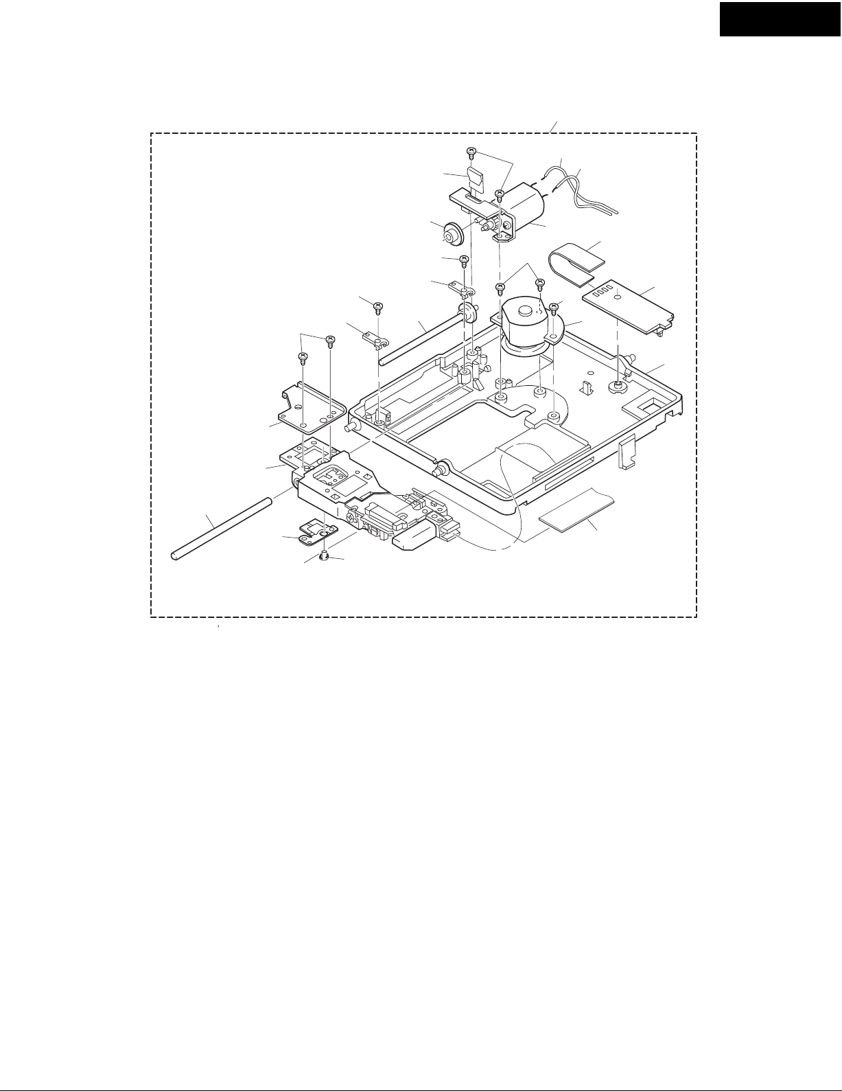
EXPLODED VIEW
MD-101A
19
P901
43
E801
46
43
17
41
F901
U5
47
Z1
P702
18
18
J10
Z5
23
U2
23
15
3
Z4
U1
Z3
8
U4
3
18
P801
21
44
23
24
1
U3
T901
5
11
15
15
27
3
39
13
11
31
32
33
3
MD-101A
3
Page 9
EXPLODED VIEW PARTS LIST
MD-101A
REF NO. PART NO. DESCRIPTION
1 27111252 Front bracket
3 838130088
5 27100411
8 27191159
11 28141489
13 27190503A
15 838430107
17 830440069
18 29110083
19 27300750
21 28184826
23 838930088
24 28141472A
27 27212354
31 28191944A
32 28191945
33 28198939
39 28325966
41 27122915
*
41 27122916 Rear panel <GT>
*
41 27122917 Rear panel <GR>
*
43 838430088
44 29362968
*
44 29360687
46 27191143
47 29362285
NOTE: THE COMPONENTS IDENTIFIED BY MARK ARE
CRITICAL FOR RISK OF FIRE AND ELECTRIC SHOCK.
REPLACE ONLY WITH PART NUMBER SPECIFIED.
[Notes]
This model may be produced in the case where it is manufactured in Malaysia, and Japan.
About the parts which have the mark on REF NO., part numbers differ by the case of the Malaysia production, and the case of
production of Japan.
When you exchange this part, check the manufacture place of the origin on the rear panel, and use the same parts.
27122915-1 Rear panel <DT>
27122916-1 Rear panel <GT>
27122917-1 Rear panel <GR>
29362968-1
3TTB+8B, Self tapping screw
Chassis
Holder, M
Cushion, Reg
KGLS-8RF, Holder
3TTB+10S(BC), Self tapping screw
4TTC+6C(BC), Self tapping screw
TAPE(CROSS-16U)
Bushing, #2271
Top cover
3TTB+8B(UN), Self tapping screw
Cushion
Front panel
Clear plate
Clear plate, RE
Facet, S
Knob, JOG
Rear panel <DT>
3TTB+8B(BC), Self tapping screw
, CLASS1 SPEC, <GR>
Label
Label,
CLASS1 SPEC, <GR>
Label, CLASS-1 <GT>
Holder <GR>
Label, caution
MANUFACTURED IN MALAYSIA
MADE IN JAPAN
MANUFACTURED IN MALAYSIA
MADE IN JAPAN
MANUFACTURED IN MALAYSIA
MADE IN JAPAN
MANUFACTURED IN MALAYSIA
MADE IN JAPAN
*
REF NO. PART NO. DESCRIPTION
E801 260208 Binder, UL
P901 253336VOL or
253335HIT
P901
P901 253333VOL or
T901 2301545
J10 1F999013UL Faston AS
P702 2045291512
P801 204417023
F901 252074
U1 1H478598-1B
U2 1H478599-1B
U3 1H478500-1B
U4 1H478501-1B
U5 1H478502-1B
Z1 24650035 KMK-260EDN, MD Mechanism
Z3 24611665
Z4 24605828
Z5 24604139A
253337HIT or
253338VOL
253332HIT
2301554
1H478598-1C
1H478598-1D
1H478599-1C
1H478599-1D
1H478500-1C
1H478500-1D
1H478501-1C
1H478501-1D
1H478502-1C
1H478502-1D
AS-CEE or
AS-CEE, Power supply cord <GT>
AS-CCEE or
AS-CCEE, Power supply cord <GR>
AS-UC-2 or
AS-UC-2, Power supply cord <DT>
NPT-1424D, Power transformer <DT>
NPT-1424G, Power transformer <GT,GR>
NCFC5-291512, Flexible flat cable
NCFC4-17023, Flexible flat cable
2A-SE-EAK , Fuse <GT,GR>
NAAR-7298-1B, Main circuit PC board ass'y <DT>
NAAR-7298-1C, Main circuit PC board ass'y <GT>
NAAR-7298-1D, Main circuit PC board ass'y <GR>
NADG-7299-1B, Microprocessor PC board ass'y <DT>
NADG-7299-1C, Microprocessor PC board ass'y <GT>
NADG-7299-1D, Microprocessor PC board ass'y <GR>
NAPS-7300-1B, Power supply PC board ass'y <DT>
NAPS-7300-1C, Power supply PC board ass'y <GT>
NAPS-7300-1D, Power supply PC board ass'y <GR>
NADIS-7301-1B, Display PC board ass'y <DT>
NADIS-7301-1C, Display PC board ass'y <GT>
NADIS-7301-1D, Display PC board ass'y <GR>
NAETC-7302-1B, AC outlet PC board ass'y <DT>
NAETC-7302-1C, AC outlet PC board ass'y <GT>
NAETC-7302-1D, AC outlet PC board ass'y <GR>
Door
Spring
Shaft
NOTE:
<DT> : Taiwanese model only
<GT> : Asian model only
<GR> : Chinese model only
MD-101A
Page 10
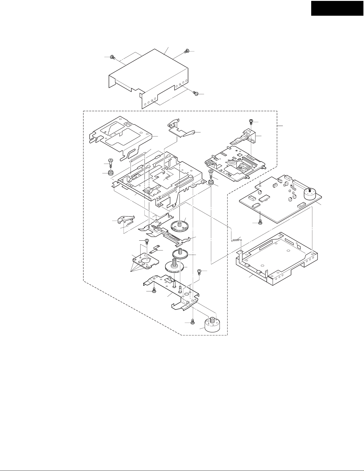
EXPLODED VIEWS OF MECHANISM-1
MD MECHANISM: KMK-260EDN
35
34
MD-101A
35
35
13
11
9
8
SW1-SW4
10
3
32
14
15
20
21
33
16
17
13
11
23
18
24
7
4
6
5
31
26
27
2
1
2
30
PARTS LIST
REF NO. PART NO. DESCRIPTIONREF NO.
10 --- Load Frame ass'y
11 2646-548-01 Insulator
13 2647-337-01 Screw, Step
14 --- Slide Frame
15 2646-559-02 Arm, head
16 2646-561-01 Spring, SP Tension
PART NO. DESCRIPTION
1 --- Motor Plate ass'y
2 7685-791-01 Screw +PTT2.6 x 5(S)
3 --- L-SW PC board
4 1792-100-21 Flexible flat cable(5 core)
5 2646-555-02 Gear(Relay B)
6 2646-554-01 Gear(Relay A)
7 X2646-726-1 Frame ass'y, slot
8 2646-563-01 Spring(Slot arm), Tension coil
9 2646-556-01 Slot Arm
17 2646-562-01 Spring, Tension coil
18 2646-560-02 Cam, mode
20 2627-529-01 Screw(+P1.7 x 2.5 Type2)
21 8620-021-71 MD Over write head
23 --- MD mount
24 7685-791-09 Screw(+PTT2.6 x 5 Type S)
26 2646-545-01 Spring(Door arm), Tension coil
27 --- Case(Lower)
30 X2626-328-1 Loading motor ass'y
31 7627-852-38 precision screw(+P1.7 x 1.8 Type 3)
32 7685-780-09 Screw +PTT2×3(S)
33 --- Loading ass'y
34 --- Case(Upper)
35 7621-259-25 Screw (+P2.6×4)
The mechanical parts with no part number
in the exploded views are not supplied.
Page 11
EXPLODED VIEW OF MECHANISM-2
MD MECHANISM: KMK-260EDN
MD-101A
69
65
64
68
66
63
57
51
67
58
56
57
52
51
51
59
55
53
54
71
61
59
60
62
70
PARTS LIST
REF. NO. PART NO. DESCRIPTION
51 3348-998-51 Pan tapping screw(M1.4×3.5)
52 2167-550-01 Plate(M), Pre load
53 --- Wire, SL motor lead
54 --- Wire, SL motor lead
55 X2162-145-1 Sled motor ass'y
56 2646-571-11 Gear(MD)
57 2167-551-01 Plate(M), main shaft fixed
58 X2162-144-1 Screw ass'y, lead
59 2646-358-11 Screw(B1.7 x 4)
60 X2162-143-1 Spindle motor ass'y
61 --- Mounted, PWD(D)SW
62 --- Chassis(M), mehanical
63 3039-041-01 Screw(M1.4 x 3)
64 2168-512-01 Plate, protection
65 2167-819-01 Shaft(M), guide
66 2647-338-01 Spring, rack
67 2627-529-01 Grip(1.7 x 2.5 type2)
68 8583-079-06 Optical pick up, KMS-260E
69 --- Deck ass'y, mechanical
70 1669-180-11 OP Flexible flat cable
71 1783-387-11 Flexible flat cable(7core)
The mechanical parts with no part number
in the exploded views are not supplied.
Page 12
EXPLODED VIEWS OF MECHANISM-3
MD MECHANISM: KMK-260EDN
MD-101A
MD Mount view
IC121
IC125
Test point-A
for adjustment
RF
VC
TE
IOP
I+3V
AGND
Side-A
IC171
IC201
D101
IC101
CN102
CN104
To over write head
CN110
Test point-B
for adjustment
RF
VC
TE
CN106
FE
IOP
I+3V
WP
CN103
Test point
(No use)
IC104
IC105
To main borad
IC301
D183
D181
To L-SW PCB
Side-B
Q162
Q102
Q101
IC103
Q103
X201
IC102
CN101
To pick-up unit
IC152
CN105
To D-SW PCB
Q182
Q181
IC181
Page 13

EXPLODED VIEWS OF MECHANISM-4
MD MECHANISM: KMK-260EDN
MD-101A
L-SW PC BOARD VIEW
SW1 SW2 SW3 SW4
CN107
The mechanical parts with no part number
PARTS LIST
REF. NO. PART NO. DESCRIPTION
IC101 8752-080-95 CXA2523AR, IC
IC102 1781-569-21 90M, oscillator
IC103 8729-903-10 FMW1-T-148, IC
IC104,IC105 8759-689-63 RH5RZ35CA-R1, IC
IC121 8752-404-64 CXD2662R, IC
IC125 8759-671-27 MSM51V4400E-70TS-K, IC
IC152 8759-574-24 BA5984FP-E2, IC
IC171 8759-640-39 BR24C02F-WE2, IC
IC181 8759-523-35 TC74ACT02FT(EL), IC
IC201 8752-926-12 CXP740010-060R, IC
IC301 6700-563-01 AK4552VT-E2, IC
Q101 8729-028-91 DTA144EUA-T106, Transistor
Q102 8729-026-53 2SA1576A-T106-QR, Transistor
Q103 8729-028-96 DTC114EUA-T106, Transistor
Q162 8729-101-07 2SB798-T1DK, Transistor
Q181 8729-018-75 2SJ278MY, Transistor
D101 223269R2 1SS355, Diode
D181,D183 8719-046-87 F1J6TP, Diode
Q182 8729-017-65 2SK1764KY, Transistor
X201 1767-179-31 12M, oscillator
CN101 1691-385-21 Connector, FFC/FPC(21P)
CN102 1778-461-11 Connector FFC/FPC(29P)
CN103,CN105,CN110 1779-345-11 Connector FFC/FPC(7P)
CN104 1778-283-11 Connector FFC/FPC(4P)
CN106 1779-353-21 Connector FFC/FPC(5P)
SW1-SW4 1771-092-21 Push switch (1key)
SW5 1771-327-11 Switch 2pin push(2key)
CN107 1785-242-21 Connector, FFC/FPC(5P)
CN108 1794-627-21 Connector, FFC/FPC(7P)
(MD mount section)
--- --- Mount, L SW
--- --- PWB, L SW
--- --- D SW mount
--- --- D SW PWB
in the exploded views are not supplied.
D-SW PC BOARD VIEW
SW5
CN108
Page 14

BLOCK DIAGRAM
MD-101A
BLK
STB
CLK
DATA
36
42
41
Q802
SUB MICROPROCESSOR
FLTUBE CONTROLLER
TMP87C44U
1
301444 33
CS
CLK
DATA
RESET
OPERATION
KEYS
LED
LED
JOG-B
JOG-A
Q801 FL TUBE
WITH DRIVER IC
HCA-14SS02T
KEY1
KEY0
76
77
36
3
2
9
10
6
8
P402A
Q803
REMOTE
SENSOR
SPS-440-1
REMO61
MAIN MICROPROCESSOR
(SYSTEM CONTROL)
23
DIN1
DIN2
AC
AC
Q703,Q704
Q713,Q705
FILAMENT
ON/OFF
27 FILAMENT
Q701
UPD78F0058GC
131912
21
20
SYSDA(SDATARC)
Q709
STOP KEY RESET
MECLK(CLK)
MERESET
MECS(RCREQ)
PDOWN
641162
60
63
SYSOUT50
51
SYSIN
LINEMUTE49
MEMUTE(AMUTE)
MDREQ
MEDATA(SDATAMD)
Q706
BUFFER
MD MECHANISM
POWER CONTROL
Q702
LEVEL SHIFT
74HCU04
MDREQ
MEMUTE(AMUTE)
MEDATA(SDATAMD)
KMK-260EDN
Q903,Q904
DRIVER
+36V(Q801,Q802)
M+5V(MD MECHA)
H+5V(MD MECHA)
+5V(DIGITAL INPUT)
3.3V(MD MECHA)
(Q701,Q702,Q709,Q802)
Q707,Q708
MUTE DRIVER
RESET(Q701)
POFF(Q701)
+5V(MD MECHA)
+5V
+B(FILTER)
-B(FILTER)
L IN
R IN
L OUT
R OUT
Q901
D902,D913
Q711
BMR0101
Q905
7805
Q906
29M05
Q907
29M33
Q902
29M05
Q101(1/2)
Q101(2/2)
POWER TRANSFORMER
D901
Q203
Q204
Q405
OPT
ON/OFF
5V
T901
DIGITAL
INPUT 1
Q401
P402
Q403
BUFFER
74HCU04
Q201,Q205
MUTE
Q202,Q204
MUTE
C902
DIGITAL
INPUT 2
Q402
L901
P101
C901
RI
REMOTE
CONTROL
P701
L
INPUT
R
ANALOG
L
OUTPUT
R
AC OUTLET
P902
P901
AC IN
MD-101A
Page 15

MD-101A
A
SCHEMATIC DIAGRAMS
NADIS-7301
U4
DISPLAY PC BOARD
1
33
GND
34
GND
35
SUB_BLK
FL_STB36
GND
37
38
GND
39
GND
VDD40
FL_DATA41
FL_CLK42
GND
43
SUB_DATA
44
S-CLK
1
R805
2
100
28
31
32
GND
GND
GND
SUB_ACK29
SUB_STB 30
Q802
TMP87PH47U
GND
GND
GND
GND
CHECK
45678
3
2
R804
100
GND
GND
R803
100
GND
GND
F1A1F1B2F1C
3
2324252627
GND
GND
GND
GND
GND
GND
GND1 19
VAREF18
VASS[GND] 17
OSC2 16
OSC1 15
RESET14
TEST[GND]13
GND
GND
GND
GND
9
10
11
BCDEFGH
NOTE
.
THE COMPONENTS IDENTFIED
REPLACE ONLY
.
Q801
HCA-14SS02T
1
INB
5V5
2
INA
OUT4
3
10K
R824
22
21
20
12
1K
R801
473
C801
R80210K
104
C804
104
C811
JOGB
P801B
C814
104
X702
8.0MHZ
LED
C802
JOGA
102
5V
Q805
TC7S00FU
4.8
GND
FLCS
REMO
FLCLK
FLDATA
FLRESET
R813
C815
C816
KEY1F2KEY0
10K
S808
EJECT
223
223
F1
S807
C809104
+VDISP
FL_CLK34
FL_DI33
FL_DO32
1K
R827 1K
R826
C817
R814
1.8K
S814
DISPLAY
SLR-332
D801
STANDBY/ON
R825
33K
C810
104
223
FL_BLK36
FL_STB35
VDD137
VDD238
1K
R8291KR828
+36
MULTI JOG
R812
3.9K
R815
1K
S813
STANDBY/ON
R820
470
VSS139
D802
NP41
VSS240
R811
1.8K
S806
YES
R816
820
S812
INPUT
R821
UDZS5.6B
F2A42
F2B43
R819
470
F2C44
R8101KR809
S805
REC
R817
470
S811
REC_MODE
100
223
C806
REMO
470
R822
C807
R818
390
104
S810
C805
820
S804
FR
CD_DUB
+4.8
100/6.3
R808
470
FF
S803
KEY1
S809
PLAY
C812
EDIT/NO
R830
1K
R807
390
S802
STOP
/PAUSE
104
Q803
SPS-440-1-N
KEY0
S801
C813
104
VOLTAGE (MEASURED WITHVOLTMETER) IS
.
ELECTROLYTIC CAPACITORS (
.
ALL CAPACITORS ARE IN pF/50WV UNLESS OTHERWISE NOTED.
EX) 030 3pF 330 33pF 331 330pF
.
ALL RESISTORS ARE IN OHMS 1/4WATTS
.
THE THICK LINES ON PC BOARD ARE THE PRINTING SIDE OF THE PARTS.
EX) PRINTING SIDE
.
CIRCUIT IS SUBJECT TO CHANGE FOR IMPROVEMENT.
POWER SUPPLY PC BOARD
U1
NAAR-7298
Q904
2SB1068
Q905
MPC2905
+5.1
P903
78
GND34
OPTOFF23
K1 77
NC424
+36
Q705 KRA107S
R734
K0 76
XT1 73
VDD0[+5VD] 74
AVREF0[+5VE] 75
UPD78F0058GC
NC525
NC626
FILAMENT27
GND728
R707
R705
R703
+VDISP
10K
72
XT2
Q701
GND829
GND930 IC[VPP] 71
1K
1K
1K
Q713
KRC107S
X701
X1 70
GND1031
+36
5.0MHz
X2 69
VDD1[+5VB] 68
VSS1[GND12]33
GND1132
PDOWN
MECS
MERESET
MECLK
SYSDA
MEDATA
R737
R738 22K
65
64
66
67
GND32
MEMUTE
SUB_ACK
VSS0[GND34]
STBYLED36
GND1334
GND1435
GND1537
Q703
22K
2SD655
Q704
5VBK
5V
63
62
REQ
POFF
GND30
GND29
GND28
GND27
GND26
GND25 54
GND24 53
GND23
SYSIN 51
SYSOUT
LINEMUTE
GND22
GND21
GND20
GND19
CHKSIG
SCHECK
JAPAN
GND1638
GND1739
61
RESET
REMIN
METEST
GND1840
R708
1.8K
2SD655
+5
R728
60
59
58
57
56
55
52
50
49
48
47
46
45
44
43
42
41
R709
10K
1.8K
C701
473
R725 47K
R720 10K
R719 10K
R718 10K
R717 10K
R745
R710
1.8K
R743 10K
Q712
KRC104S
C708 223
R912
390
0
R711
1.8K
C702
R712
473
1.8K
C707
1/50
1SS352
D705
C922
104
C923
220/6.3
Q706
KRA107S
R726 330K
UDZS5.6B
Q711
BMR0101
OUT
R740 22K
D911
1SS352
D912
GP104003E
D702
1SS352
D701
10K
R723
To P402
R718: MGR,MGT,
MDT only
R745: MJJ only
VCC
R715
330
R739
4.7K
10K
R910
R716 10K
P402A
OPT OFF
C928
R909 470
473
D903
C909
R721
470
223
UDZS5.1B
R714
10K
6
78
GND
Q702
9
R713
330
R722
470
P903A
+5.8
4
5
74HCU04
101112
5.6V
3
+0.26
R729
3
2
10K
5
6
R730
2
13
C929
3
NADG-7299
U4
MICROPROCESSOR
P801A
JOGB
F2
F1
REMO
FLCLK
FLDATA
FLRESET
KEY0
KEY!
FLCS
LED
JOGA
5V
PC BOARD
R735
2.7K
R736
2.7K
REMO
4
R002
2.2K
R001
2.2K
FLASH0
FLASH1
RESET
5V
IC
P001
for
SOFT VERSION UP
R701
2.7K
R702
2.7K
5
1
GND
ROTEN12
ROTEN23
AVSS[GND]4
GND25
SUB_STB6
AVREF1[+5VA]7
SUB_RESET8
SUB_DATA9
SUB_CLK10
MEDA11
SYDA12
MECLK13
FLASH114
FLASH215
GND316
GND417
GND5
18
MERESET
19
20
MECS
R706 1K
R704 1K
SHUT
80
21
79
GND35
GND36
NC222
DOWN
DOUT
MGND2
DIN0
DIN1
M+5VB
MGND1
MD MECHANISM
CLK
M+5VA
HGND
SDATAMD
H+5V
SDATARC
RCREQ
Page 16

WITH PART
C910
+5.8
ARE CRITICAL FOR SAFETY.
MARKBY
NUMBER SPECIFIED.
ARE IN F/WV.
u
)
333 0.033uF
UNLESS OTHERWISE NOTED.
C920
D910
Q902
10/16
G
IO
MPC29M05
100/6.3
DCVOLTAGE.
+VDIS
D914
1SS352
22/16
C908
(NO INPUT SIGNAL)
Q901
KTD863
+36
4.7/50
UDZS18B
R905 100
R906 100
C913
D902
UDZS18B
D913
+10.2
22000/16
R904
R916
D904
D905
33K
C907
[NOTES]
MJJ : Japan model
MDT : Taiwanese model
MGR : Chinese model
MGT : Korean model
Q908
KRA107S
3.3K
47/50
D906
RS403M
Q909
KRC107S
C911
C906
MD-101A
AC OUTLET PC BOARD
U5
MGT
NAETC-7302
F901
T2AL250V
J1B J2B
+42
D901
GP104003E
C905
47/50
224
C904
R915
33K
JL901B
D901,D906-D909
RL1N4003
or GP104003E
334
C903 473
JL901A
F1
F2
AC2
GND
AC1
C951
473
NC
P902
T901
AC OUTLET
NAPS-7300
J1A
L901
C901
C902
C901,C902
MJJ
103Z
MDT
103M
MGR, MGT
472M
MJJ,MGR,MDT
NAETC-7302
P902
J1B
J2B
U3
POWER TRANSFORMER
PC BOARD
J2A
P901
AC OUTLET
AC IN
MJJ : 100V 50/60Hz
MGT,MGR : 230V 50/60Hzz
MDT : 120V 60Hz
R729
Q904
Q905
+5.1
10K
2
13
R907
IO
G
MPC2905
470/6.3
3
2
8
5
6
4
470
R730
1
Vcc
C929
100/6.3
22K
C917
1
Q709
NJM4565M
Q709
7
473
C925
C703
R908
1.5K
R917
1.5K
10/16
D703
1SS352
104
C926
L902
Q903
D704
1SS352
C927
10/16
R724
100
KRC107S
C706
Q710
KRC107S
R731
R732
Q708
1SS352
L903
L904
223
82K
100
C704
C705
470K
D706
+5.0
100/16
100/16
R744
Q707
KRA107S
L905
Q906
MPC29M05
IO
G
C918
470/6.3
KRA107S
MPC29M33
Q907
IO
G
+3.3
220/6.3
RI
POWER CONT
C919
P905
P905A
C914
2200/16
-11.0
C912
334
DIN0
DIN1
KRA107S
OPT OFF
Q405
C405
P402
To P402A
1.2K
R110
R105
390
(1/2W)
R106
390
(1/2W)
LIN
1.2K
R109
-2.8
D102
D101
R107
UDZ2.4B
UDZ2.4B
+2.8
1.8K
R108
1.8K
C106
C105
C103
22/50
22/50
C104
100/6.3
100/6.3
RIN
P906
P906A
LIN
RIN
R914
120 (1/2W)
R408
1K
R407
1K
R406 470
R405 470
74HCU04
223
1
NJM2100
7
Q101
8
Q101
9
10
11
12
13
Vcc
14
4
2
3
5
6
C403
C101
C102
104
C404
100/6.3
R401
R403
100K
R404
C932
BL02RN2-R62
R727
470
100K
473
100
R402
100
L701
LOUT
ROUT
Q403
GND
78
6
5
4
3
2
1
R101
18K
22K
101
R103
101
22K
R104
R102
18K
C709
101
C401
C402
C933
Q401
1
104
DIGITAL INPUT
OPTICAL
Q402
2
104
C710
P701
473
RI
C711
473
473
P101
L
INPUT
R
ANALOG
L
OUTPUT
R
P102
P102A
120
R913
1.5K
R221
D201
UDZS4.7B
R222 1.5K
(1/2W)
C915
+9.1
470/16
+4.3
473
C213
R741
220K
104
C214
R742
330K
C916
470/16
R229
R217
R218
R230
100
100K
100K
100
R219
R220
-9.5
-B
5
6
27K
27K
6
5
NJM4565M
Q203
R203
27K
C203
101
27K
R201
27K
R202
C204 101
R204 27K
Q204
NJM4565M
R205
R207
1.2K
822
822
R208
1.2K
470
C207
822
C208
822
NJM4565M
R209
1.5K
C209
C210
R210
1.5K
102
102
2
3
3
2
4
Q203
8
NJM4565M
8
Q204
4
R225
R211
R212
100K
100K
2.2K
R213
470
2.2K
R215
2SD655
2.2K
R216
R214
470
R226 2.2K
Q205
Q206
2SD655
C211
47/50
1
1
C212
47/50
MUTE
7
470
C205
C206
R206
7
R227
470
2SD655
R228
ROUT
LOUT
Q201
Q202
2SD655
470
H+5V
SDATARC
RCREQ
MDREQ
PWRCNT
5VB
3.3V
RESET
AMUTE
PDOWN
KMK-260EDN
5VA
LIN
SPL/XSPD
C930
104
RIN
GND1
ROUT
LOUT
AGND2
P702
AGND1
Page 17

PC BOARD CONNECTION DIAGRAM
MD-101A
AC IN
U5
NAETC-7302
AC outlet
PC board
AC-H AC-G
P901
U3
NAPS-7300
Power supply
PC board
J1A
J2A
J2B
J1B
DIGITAL INPUT
2
1
Q401
U1
P402
NAAR-7298
Main circuit PC board
P904
C913
JL901B
For MD
adjustment
Q402
RI
REMOTE
CONTROL
ANALOG
OUTPUT
Q906
Q905
Q902
INPUT
Q907
P102
P906
P905
P903
ROUT
GND
LOUT
GND
-11V
GND
GND
GND
+10.2V
GND
LIN
GND
RIN
RI
+3.3V
GND
-5.0V
POWER CONT
GND
+5.1V
GND
+5.1V
+36V
F1
F2
POFF
GND
+5.8V
P102A
P906A
U2
NADG-7299
Microprocessor
P905A
PC board
P903A
P702
T901
Power transformer
AC1
GND
JL901A
Remote sensor
GND
AC1
AC2F2F1
STANDBY/ON
Q803 NCDIS-7301
D801
DISPLAY
Q801
2
2
S814
STANBY/ON
S813
CN110
DOUT
MGND1
MGND2
S812
INPUT
1
FL tube
Sub microprocessor
CN102
CLK
DIN0
DIN1
M+5VB
M+5VA
HGND
SDATAMD
H+5V
SDATARC
RCREQ
MDREQ
KMK-260EDN
MD Mechanism
FLDATA
FLCLK
+VDISP
KEY1F2KEY0
F1
P801B
25137301
X702
Q802
LIN
RIN
5VA
5VB
PDOWN
PWRCNT
FLRESET
REMO
RESET
FLCS
GND
3.3V
AMUTE
SUB_ACK
GND
LP_MODE
5V
JOGA
LED
22
GND1
SPL/XSPD
JOGB
S810S811
CD_DUB
ROUT
U4
NADIS-7301
Display PC board
AGND2
NO
2
LOUT
S809
AGND1
P801B
REC
YES
222
S806
S805
2
Main microprocessor
S808
MULTI JOG
S807
S807
FR
FF
S803
2
S804
2 2
2
PLAY
S801
S802
STOP
XOPT-DIN1
Q701
X701
DIN2
GND
C922
P402A
P801A
P001
Page 18

MD-101A
A
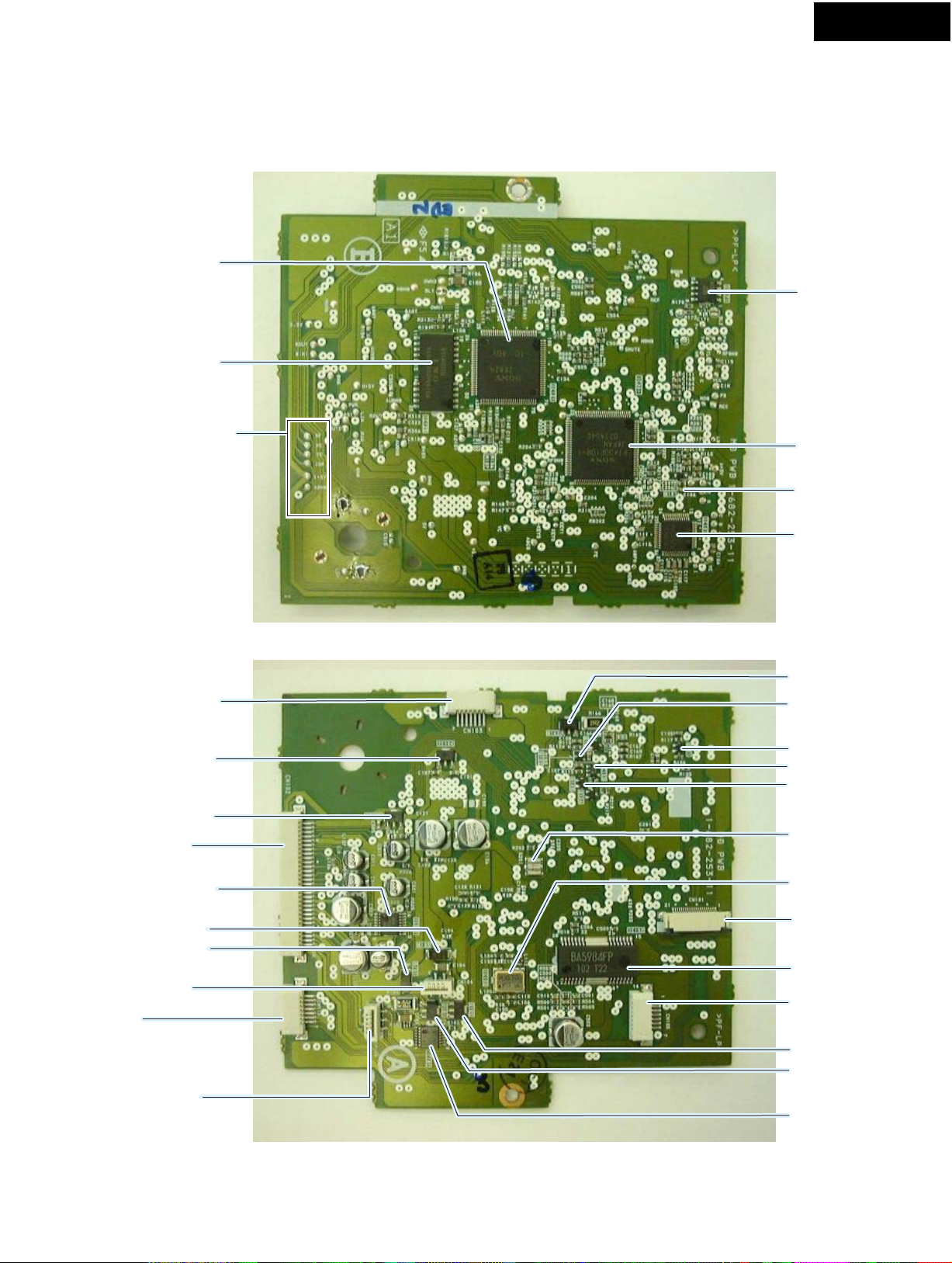
PRINTED CIRCUIT BOARD VIEWS-1
S808
J205
C812
R825
D802
R824
R829
EJ
PLAY
C801
R826
S803
2 2
R802
J203
R817
R828
P801B
J204
YES
222
S807
S807
FR
FF
2
2
S802
STOP
R801
C802
R821
R803
C814
S805
S804
S801
23
S806
7
J202
J201
2
REC
7
12
Q802
1
Soldering side
R522
C804
R525
R811
R521
R528
R523
R822
C809
C810
R818
C807
R527
R526
R524
C816
R809
R807
C815
R810
C813
R808
C811
R812
R813
2
C817
3
BCD
U4
DISPLAY PC BOARD
(NADIS-7301)
Component side
S810 S811
S809
2 2
2
7
J196
CD_DUB
7
J197
20
LP_MODE
E855
CUSHION
J191
15
R804
R805
1
Q805
44
R827
7
J187
J188
E854
CUSHION
R819
R814
S812
1
INPUT
Q801
NCDIS-7301
C806
J185
J184
R830
R820
25137301
J183
R815
X702
12
J189
12
J190
J186
Q801
R816
C805
Q803
J181
STANBY/ON
2
2
S814
DISPLAY
VCC
VOUT
S813
GND
D801
J200
J195
Q802
NO
12
J198
J199
J192
J193
J194
34
U3
POWER TRANSFORMER PC BOARD
(NAPS-7300)
Component side
AC-H AC-G
T901
C903
JL901A
L901
L901
C902
223 OR6
T901
U5
AC OUTLET
PC BOARD
P901
AC-GAC-H
C901
(NAETC-7302)
F901B F901A
15
4
J1B
J952
J951
15
F901
T2AL250V
25137302
NCETC-7302
J2B
J1A
J2A
NCPS-7300
1
25137300
P902
0
P902
Soldering side
C951
5
Page 19

MD-101A
A
PRINTED CIRCUIT BOARD VIEWS-2
U2
1
2
3
4
5
MICROPROCESSOR PC BOARD
(NADG-7299)
Component side
E851
Q206
PDOWN
MDREQ
SUB_ACK
REMO
FLCLK
KEY1
KEYO
LOUT
ROUT
DOUT
JOG
JOG
GND
-VB
E852
RIN
3.3V
SDA
SDA
CLK
DIN
DIN
C206
C210
LIN
5V
C212
J152
J151
J150
J149
J148
J147
J146
AGND
AGND
GND
SPL/XSPD
5V
AMUTE
RESET
PWRCNT
RCREQ
H+5V
HGND
M+5V
M+5V
MGND
MGND
J116
J114
J112
LED
5V
GND
FLCS
FLRECET
FLDATA
F2
F1
P801A
P001
P702
20
E853
22
C208
C204
J120
J117
J153
C929
J110
J159
12
12
12
15
J156
L904
J101
C205
L905
J130
L902
J129
L903
P402A
15
15
12
C211
C704
J115
J113
J157
J111
C209
J133
7
7
J121
J103
C214
C707
7
7
7
7
7
J162
J163
Q205
C207
C916
C203
7
C915
J158
20
J144
J145
C705
C925
C927
Q711
J137
J136
J135
J134
12 7
J124
C922
15
J118
J107
J102
777
J105
J106
20
J104
R913
J108
7
C916
C915
J143
J141
J125
J123
7
J154
20
7
7
J122
X701
J160
Q201
17
R914
J142
12712712
J139
J138
J131
12
7
Q202
P102A
12
J161
P906A
P905A
17
J140
P903A
7
J132
Q704
D912
C923
NCDG-7299
25137299
1
BCD
Soldering side
Q708
R742
Q703
J127
J128
J126
J119
D706
R206
R208
R210
R509
Q707
R214
R213
R211
R212
R205
R207
R209
R204
R218
8
Q204
R217
Q203
R219
R201
1
R229
R202
1
R220
R230
R508
Q709
8
R729 R730
D703
R731
R732
D704
C706
1
Q710
R740
D705
C930
C703
Q702
C928
R721R722
7
7
7
R503
R912
R735
R736
R701
R702
5V
J109
R704
R703
ICIC5V
R713
R709
R001R002
R708
8
C926
Q712
R716
14
1
R203
R715
R724
R215
C708
R744
Q702
R734
R216
R226
R741
R228
R227
R225
R222
R221
C213
D201
D903
C909
R910
R739
R909
R507
R743
R737
R738
21
R712
Q705
D702
Q706
R745
R720
R723
41
R707
C702
D911
R714
Q713
R505
R504
R506
R718
R717
R719
D701
R726
R725
C701
R728
61
80
Q701
1
Q701
R705
R706
R502
R711
R710
Page 20

MD-101A
A
PRINTED CIRCUIT BOARD VIEWS-3
U1
1
2
POWER SUPPLY PC BOARD
(NAAR-7298)
Component side
J924
P701
12
7
P102
C403
L701
R106
C106
J917
J922
J923
J921
J920
C101
C105
P402
C914
C914
R105
15
17
15
J918
25
C103
C104
C102
J916
P701
Q401
Q402
Q401
Q402
P101
P101
BCD
P904
C913
15
15
J912
Q907
7
J910
7
J908
C919
C918
7
J909
J911
D906
P905
7
JL901B
C911 C912
7
J906
Q905
Q906
J905
7
J904
C917
Q904
D901
17
J901
C910
C905
J903
C906
Q901
J902
Q902
C920
P903
C904
7
J907
C907
C908
7
J919
J914
1
J915
25137298A
NCAR-7298
P906
C913
J913
3
Soldering side
R403
1
7
R401
Q403
Q403
C401
R402
4
C933
C709
C710
C711
C932
R727
R404
C402
14
8
R501
C404
D102
R101
R103
R405
C405
Q405
Q101
R104
R406
D101
R408
R407
R915
R916
Q908
R904
R905
R906
D904
D905
R107
R109
1
R102
R108 R110
R917
D913
D902
R908
R907
Q909
D914
D910
5
Q903
Page 21

PRINTED CIRCUIT BOARD PARTS LIST-1
U1
MAIN CIRCUIT PC BOARD (NAAR-7298-1B/1C/1D)
CIRCUIT NO.
Q101
Q401,Q402
Q403
Q902,Q906
Q905
Q907
Q405,Q908
Q901
Q903,Q909
Q904
D101,D102
D901
D902,D913
D904,D905,D914
D906
L701
C103,C104
C105,C106,C910
C904
C905,C906
C907
C908
C911,C912
C913
C914
C917,C918
C919
C920
R105,R106
P101
P701
JL901B
P102
P402
P903
P905,P906
Q902A
Q905A
Q906A
Q902B,Q906B
PART NO.
ICs
22240608R1
24120083 or
24120086
222740046R2TO
22278005ENE
22278005DNE
22278033ENE
Transistors
2216480R2 or
2216350R2
2211853 or
2216605 or
2216604
2216470R2 or
2216340R2
2212855 or
2212853
Diodes
224490240R2
22380260 or
22380035
224551800R2
223234R2 or
223269R2
22380022F or
22380271F or
22380285F
Coil
230906
Capacitors
354782209
354721019
374722244
354784709
354780479
354742209
374723344
3504348
354742229S
354724719
354722219
354741009
Resistors
443523914
Jacks
25045594
25045601
Socket
25050271
Plugs
25055804
25055149
25055702
25055705
Others
27160484
27160472
27160227
82143010
DESCRIPTION
NJM2100M
GP1FA550RZ
GP1FA551RZ
TC74HCU04F
MPC29M05HF
MPC2905HF
MPC29M33HF
DTA114YKA or
KRA107S
2SD667-C or
KTD863-GR or
KTD863-Y
DTC114YKA or
KRC107S
2SB1068-U or
2SB1068-K
UDZ2.4B
RL1N4003 or
GP104003E
UDZS18B
1SS352 or
1SS355
RBV402 or
D3SBA20 or
RS403M
BL02RN2-R62, EMI filter
CE04W50V-22uF, Elect.
CE04W6.3V-100uF, Elect.
ECQ-V50V-224J, Plastic
CE04W50V-47uF, Elect.
CE04W50V-4.7uF, Elect.
CE04W16V-22uF, Elect.
ECQ-V50V-334J, Plastic
CE69W16V-22000M(LQ), Elect.
CE04W16V-2200uF, Elect.
CE04W6.3V-470uF, Elect.
CE04W6.3V-220uF, Elect.
CE04W16V-10uF, Elect.
RS1/2WBJ-390 ohm
NPJ-4PDWR405
NPJ-2PDB409
NSCT-7P99
NPLG-4P760
NPLG-5P133
NPLG-6P658
NPLG-9P661
RAD-153
RAD-141
(RAD-076), Heat sink
3P+10FN(BC), Pan head screw
MD-101A
NOTE:
<DT> : Taiwanese model only
<GT> : Asian model only
<GR> : Chinese model only
NOTE : THE COMPONENTS IDENTIFIED BY MARK
ARE CRITICAL FOR RISK OF FIRE AND
ELECTRIC SHOCK. REPLACE ONLY WITH
PART NUMBER SPECIFIED.
Page 22

PRINTED CIRCUIT BOARD PARTS LIST-2
MICROPROCESSOR PC BOARD (NADG-7299-1B/1C/1D)
U2
CIRCUIT NO.
Q203,Q204,Q709
Q701
Q702
Q711
Q201,Q202
Q205,Q206
Q703,Q704
Q705,Q706,Q707,Q708
Q710,Q713
Q712,Q804
D201
D701
D702-D706
D903
D910-D911
D912
L902-L905
X701
C101,C102,C203,C204
C205-C208
C209,C210
C211,C212
C214
C403,C929
C704,C705
C707,C808
C915,C916
C922
C923
C925,C927
R913,R914
P904
P102A
P402A
P702
P801A
P903A
P905A,P906A
E852,E853
E854,E855
Q905
PART NO.
ICs
22241383R2
22241670R3
222740046R2TO
22241210
Transistors
2211705 or
2211706
2211705 or
2211706
2216350R2 or
2216480R2
2216470R2 or
2216340R2
2214770R2 or
2216210R2
Diodes
224550470R2
224550560R2
223234R2 or
223269R2
224550510R2
223234R2 or
223269R2
22380260 or
22380035
Coils
230906
Oscillator
3010343
Capacitors
374721015
374728224
374721024
354784709
374721044
354721019
354741019
354780109
354744719
3000120
354722219
354741009
Resistors
443521214
Terminal
25060140
Sockets
25051526
2009990681UL
25052523 or
25052329
25052317 or
25052511
25051231
25051234
Others
27190540-1
28141471
82143010
DESCRIPTION
NJM4565M-D
MPD780056GC-038-8BT
TC74HCuF04F
BMR-0101D
2SD655-E or
2SD655-F
2SD655-E or
2SD655-F
KRA107S or
DTA114YKA
DTC114YKA or
KRC107S
DTC144EK or
KRC104S
UDZS4.7B
UDZS5.6B
1SS352 or
1SS355
UDZS5.1B
1SS352 or
1SS355
RL1N4003 or
GP104003E
BL02RN2-R62, EMI filter
CSTS0500MG06, Ceralock
ECQ-B50V-101K, Plastic
ECQ-B50V-822J, Plastic
ECQ-B50V-102J, Plastic
CE04W50V-47uF, Elect.
ECQ-V50V-104J, Plastic
CE04W6.3V-100uF, Elect.
CE04W16V-100uF, Elect.
CE04W50V-1uF, Elect.
CE04W16V-470uF, Elect.
FMC0H104Z, Super
CE04W6.3V-220uF, Elect.
CE04W16V-10uF, Elect.
RS1/2WBJ-120 ohm
NTM-1S68, Terminal
NSCT-4P1313
NSAS-10P0947
NSCT-29P2420 or
NSCT-29P2226
NSCT-17P2214 or
NSCT-17P2408
NSCT-6P1021
NSCT-9P1024
(CLAMP)
Cushion
3P+10FN(BC), Pan head screw
MD-101A
NOTE:
<DT> : Taiwanese model only
<GT> : Asian model only
<GR> : Chinese model only
NOTE : THE COMPONENTS IDENTIFIED BY MARK
ARE CRITICAL FOR RISK OF FIRE AND
ELECTRIC SHOCK. REPLACE ONLY WITH
PART NUMBER SPECIFIED.
Page 23

PRINTED CIRCUIT BOARD PARTS LIST-3
POWER SUPPLY PC BOARD (NAPS-7300-1B/1C/1D)
U3
CIRCUIT NO.
L901
C901,C902
P901A
JL901A
DISPLAY PC BOARD (NADIS-7301-1B/1C/1D)
U4
CIRCUIT NO.
Q801
Q803
Q802
Q805
D801
D802
X702
C805
S807
S801-S814
P801B
PART NO.
Coil
231287
Capacitors
3300030
3300031
Plug
25055675
Holder
25051111
PART NO.
FL Tube
212220
Remote sensor
241339
ICs
22241671R3
22241158R2
Diode
225338
224550560R2
Oscillator
3010341
Capacitor
355721019
Rotary encoder
25065621
Push switches
25035699
Socket
25052354 or
25052538
DESCRIPTION
NCH-3567, Choke coil
DE1307E472M-KH, IS <GT,GR>
DE1607F103M-KH, IS <DT>
NPLG-2P631
NSCT-7P898, Wire holder
DESCRIPTION
HCA-14SS02T
SPS-440-1-N
TMP87C447uF-3GC6
TC7S00FuF
SLR-332VR, LED
UDZS5.6B
CSTLS800MG56, Ceralock
CE04W6.3V-100uF, Elect.
EC11E18244, Rotaly encoder
NPS-111-S662
NSCT-17P2251 or
NSCT-17P2435
MD-101A
AC OUTLET PC BOAD (NAETC-7302-1B/1C/1D)
U5
CIRCUIT NO.
F901A, F901B
P902
PART NO.
Fuse holders
25052133
Sockets
25051637
25051990
25052611
DESCRIPTION
NSCT-1P2031 <GT,GR>
NSCT-2P1424 <GT>
NSCT-2P1777 <DT>
NSCT-2P2508, AC Outlet <GR>
NOTE:
<DT> : Taiwanese model only
<GT> : Asian model only
<GR> : Chinese model only
NOTE : THE COMPONENTS IDENTIFIED BY MARK
ARE CRITICAL FOR RISK OF FIRE AND
ELECTRIC SHOCK. REPLACE ONLY WITH
PART NUMBER SPECIFIED.
Page 24

FL TUBE VIEW
Q801:HCA-14SS02T
12G 11G 10G 9G 8G 7G 5G6G 4G 3G 2G 1G
ARTIST
MD-101A
CD-RW SKIP ON
FINALIZE
13Ga 13Gd13Gc13Gb
5
6
7
ARTIST
8
9
10
11
14Ga 14Gd14Gc14Gb
13G
(13G)
CD
23
-R W
24 25 26
SKIP ON
27
19 20 21 22
FINALIZE
16
17 18
14 15
12 13
(14G)
28 27 26 25 24 23 22 21 20 19 18 17
29
30
14G
(12G - 1G)
1 2 3 4 5
6 7 8 9 10
11 12 13 14 15
16 17 18 19 20
21 22 23 24 25
26 27 28 29 30
31 32 33 34 35
31
35
34
16 15 14 13 12 11 10 9 8 7 6 5
33
32
Page 25

MICROPROCESSOR CONNECTION DIAGRAM
MD MECHANISM
KMK-260EDN
P DOWN
RCREQ
RESET
SDATARC
MULTI JOG
EJECT
STANDBY
DISPLAY
FL BLK 36
FL STB 35
FL CLK 34
FL DI 33
Q801
FL TUBE with
built-in driver IC
HCA-14SS02T
F2
F1
/ON
PUSH
INPUT
Q805
CLK
a
b
d
c
e
RECYES
FR
FF
CD
REC
DUBBING
MODE
33 SUB BLK
36 FL STB
42 FL CLK
41 FL DATA
EDIT/NO
SUB_ACK 29
SUB_STB 30
RESET 14
SUBDATA 44
Q802
SUB
MICROPROCESSOR
TMP87C447uF-3GC6
Q704
Q703
PLAY
/PAUSE
STOP
SCLK 1
+36V
(+VDISP)
Q705
Q713
FL Tube Filament
to Power supply Circuit
+5 V
f
e
d
c
b
f
a
A MUTE
MDREQ
Q702
1
9
10
1
2
3
4
5
6
7
8
9
10
11
12
13
14
15
16
17
18
19
20
BUFFER
74HCV04
2
3
8
5
12
11
GND
ROTEN1
ROTEN2
AVSS
NU
SUB_STB
AVREF1
SUB_RESET
SUB_DATA
SUB_CLK
MEDA
SYSDA
MECLK
FLASH1
FLASH2
MU
NU
NU
MERESET
MECS
4
6
13
80797877767574737271606968676665646362
NUNUNU
SHUT_DOWNNUOPT OFFNUNUNUFILAMENTNUNUNUNUNUVSS1NUNU
21222324252627282930313233343536373839
L IN
R IN
L OUT
R OUT
D IN1
Q711
BNR0101
RESET
5.0 MHz
OSC
X2
VSS0
VDD1
D IN2
SUB_ACK
RESET
NU
ME MUTE
K1
SDATA MD
+5 V
K0
POWER
SUPPLY
CIRCUIT
+5 V
VDD0
AVREF0
NU
Q709
BUFFER
XT2
IC(VPP)
X701
X1
Q701
MAIN MICROPROCESSOR
MPD780056GC-033-8BT
[NOTES]
NU: NO USED
STBY_LEDNUNUNUNU
Q712
POFF
Rch
Q710
61
REQ
REMIN
LINE MUT
Rch
RESET
RESET
NU
NU
NU
NU
NU
NU
NU
NU
SYS IN
SYS OUT
NU
NU
NU
NU
CHKSIG
CHECK
JAPAN
METEST
40
Q203(2/2)
+3.3 V
Q708
60
59
58
57
56
55
54
53
52
51
50
49
48
47
46
45
44
43
42
41
Q101(1/2)
BUFFER AMP
Q203(1/2)
4
6
Q707
BUFFER
74HCU04
3
512
Q205
Vcc
2
14
1
13
+4.8 V
Q403
+5 V
Q803
REMOTE
SENSOR
Q706
BUFFER
+5 V
INITIALIZE
Setup of the destination
R718,R745
MUTE
Q201
Q404
OPT OFF
Rch
Rch
+5 V
P101
L
R
L
R
Q401
Q402
P701
+4.8 V
STANDBY/ON
LED
MD-101A
INPUT
ANALOG
OUTPUT
1
DIGITAL
INPUT
OPTICAL
2
RI
REMOTE
CONTROL
MD-101A
Page 26

MICROPROCESSOR TERMINAL DESCRIPTIONS-1
Q701: MPD780056GC-033-8BT (MAIN MICROPROCESSOR)
MD-101A
PIN NO.
1
2
3
4
5
6
7
8
9
10
11
12
13
14
15
16
17
18
19
20
21
22
23
24
25
26
27
28
29
30
31
32
33
34
35
36
37
38
39
40
FUNCTION FUNCTION
Not used. (Connect to ground)
NOT USED (GND)
ROTEN1
ROTEN2
AVSS
NOT USED
SUB STB
AVREF1
SUB RESET
SUB DATA
SUB CLK
MEDA
SYDA
MECLK
FLASH1
FLASH2
NOT USED(GND)
I
Pulse input terminal from rotary encoder (MULTI JOG).
I
I
Negative power supply input terminal for D/A converter.
I
Not used.
I
Output terminal of tip selection for serial communication with sub microprocessor.
O
Reference voltage input terminal for D/A converter.
---
Reset signal output terminal to sub microprocessor.
O
O
Serial data output terminal to sub microprocessor.
Clock output terminal for serial communication to sub microprocessor.
O
Serial data input terminal from MD mechanism.
I
Serial data output terminal to MD mechanism.
O
Clock output terminal for the serial communication with MD mechanism.
O
Input terminal for writing at the time of flash microprocessor use.
I
I
Not used. (Connect to ground)
I
I
I
MERESET
MECS
SHUT DOWN
NOT USED (OPEN)
OPT OFF
NOT USED (OPEN)
Reset output terminal for MD mechanism.
O
Signal output terminal for serial communication with MD mechanism.
O
Power failure detected signal output terminal to MD mechanism.
O
Not used. (Open)
O
Output terminal for control of the optical digital input.
O
Not used. (Open)
O
O
O
FILAMENT
NOT USED( GND)
Output terminal for filament control of FL tube.
O
Not used. (Connect to ground)
I
I
I
I
I
VSS1
NOT USED (GND)
Negative power supply input terminal. (Connect to ground)
I
Not used. (Connect to ground)
I
I
STBYLED
NOT USED (GND)
Output terminal for control of STANDBY/ON LED.
O
I
Not used. (Connect to ground)
I
I
I
PIN NO.
41
42
43
44
45
46
47
48
49
50
51
52
53
54
55
56
57
58
59
60
61
62
63
64
65
66
67
68
69
70
71
72
73
74
75
76
77
78
79
80
METEST
JAPAN
CHECK
CHKSIG
NOT USED (GND)
LINEMUTE
SYSOUT
SYSIN
NOT USED (GND)
RESET
REMIN
REQ
POFF
ME MUTE
NOT USED (GND)
SUB ACK
VSS0 (GND)
VDD1
X2
X1
IC (VPP)
XT2 (OPEN)
XT1
VDD0
AVREF0
K0
K1
NOT USED (GND)
I/OI/O
DESCRIPTIONDESCRIPTION
The input terminal for test mode setup of MD mechanism.
I
Input terminal for carrying out initial setting of the destination
I
Input terminal for setting up the check mode of the program
I
Signal output terminal for check of program.
O
Not used. (Connect to ground)
I
I
I
I
Output terminal for muting circuit control
O
System control (RI) signal output terminal.
O
System control (RI) signal input terminal.
I
Not used. (Connect to ground)
I
I
I
I
I
I
I
I
Input terminal of system reset.
I
Input terminal of the remote control signal from the remote sensor.
I
Signal input terminal for communication with MD mechanism.
I
Input terminal of power failure detected signal.
I
Muting signal input terminal from MD mechanism.
I
Not used. (Connect to ground)
I
Signal input terminal of the completion of serial data reception from the sub microcomputer
I
Negative power supply input terminal of the port part.
---
Positive power supply input terminal.
--O
Connection terminal of the oscillation element of main system clock. (5MHz)
I
Internal connection terminal.
I
O
Sub system clock oscillation element connection terminal.
I
Positive power supply input terminal of port section.
---
Reference voltage input terminal of A/D converter.
I
I
Input terminal from operation keys. (Inputs by A/D conversion.)
I
I
Not used. (Connect to ground)
I
I
MD-101A
Page 27

MICROPROCESSOR TERMINAL DESCRIPTIONS-2
Q802: TMP87C447uF-3GC (SUB MICROPROCESSOR)
MD-101A
PIN NO.
1
2
3
4
5
6
7
8
9
10
11
12
13
14
15
16
17
18
19
20
21
22
FUNCTION DESCRIPTION
SUB_CLK
NOT USED
NOT USED
NOT USED
CHECK
NOT USED
NOT USED
NOT USED
NOT USED
NOT USED
NOT USED
NOT USED
TEST
RESET
OSC1
OSC2
GND
WAREF
NOT USED
NOT USED
NOT USED
NOT USED
I/O
I
Input terminal of serial data clock from main microprocessor.
---
Not used. (Connect to ground)
---
---
Check terminal.
O
Not used. (Connect to ground)
---
---
---
---
---
---
--I
Test terminal.
Input terminal of system rest.
I
I
Connection terminal of the oscillation element.
O
---
Negative power supply input terminal of A/D converter.
---
Reference voltage input terminal of A/D converter.
Not used. (Connect to ground)
---
---
---
---
PIN NO.
23
24
25
26
27
28
29
30
31
32
33
34
35
36
37
38
39
40
41
42
43
44
FUNCTION DESCRIPTION
NOT USED
NOT USED
NOT USED
NOT USED
NOT USED
NOT USED
SUB_ACK
SUB_STB
NOT USED
NOT USED
NOT USED
NOT USED
NOT USED
FL STB
NOT USED
NOT USED
NOT USED
VDD
FL DATA
FL_CLK
NOT USED
SUB_DATA
---
Not used. (Connect to ground)
---
---
---
---
--O
Output terminal which gives the completion notice of data receipt to main microcomputer.
Input terminal of the STB signal from the main microcomputer
I
---
Not used. (Connect to ground)
---
---
---
--O
Output terminal of the STB signal to the FL display driver IC.
---
Not used. (Connect to ground)
---
---
--O
Output terminal of the serial data to the FL display driver IC.
Output terminal of the serial clock to the FL display driver IC.
O
---
Not used. (Connect to ground)
I
Input terminal of the serial data from the main microprocessor.
MD-101A
Page 28

ADJUSTMENT PROCEDURES-1
The necessity for adjustment
necessary
Adjustment item
Adjustment of Temperature Compensation Offset
1
Adjustment of laser power
2
Check of laser power
3
Adjustment of Traverse (EF balance)
4
Check of error rate in high reflectance disk
5
6
Check of error rate in low reflectance disk
7
Adjustment of focus Bias
8
Check of focus bias
unnecessary
Pickup unit
The exchanged parts
Parts on MD
mount,
and Motors
Mechanical
parts
MD-101A
REMARKS
When an error rate is worse than
the standard value, perform this
work.
Notes in adjustment
1. Laser of pickup
In case adjust, don't look at the laser of the pickup unit.
You have fear of loss of eyesight.
2. Perform adjustment using test mode.
3. Perform adjustment as the indicated turn.
4. After adjustment should cancel test mode.
Equipment required for adjustment
1. Measuring instrument
Name
Laser power meter
Optical sensor
Oscilloscope
Digital volt meter
2. T est disk
Name
MO disk
High reflectance disk
Manufactured
LEADER
LEADER
Manufactured
Description
LPM-8010
LP-8010-02
Frequency range is 40MHz or more.
The calibration of the probe is performed.
Description
Standard disk for recording/play back
A-BEX TMD-381
3. JIG
Name
Extended JIG
Flexible flat cable
0J12
0F001
DetailsPart No.
PC board
FFC socket
1mm pitch, 7 cores
Part No. NCJIG-0J12
Part No. 25052307
Page 29

ADJUSTMENT PROCEDURES-2
Explanation in test mode
1. How to test mode to enter
(1) Connect the power supply cord in the wall socket.
(2) While hold down the YES button, press the DISPLAY button
at standby state.
(3) Release only the DISPLAY button, with press the YES button.
(4) Press the STANDBY button, with press the YES button.
(5) Release the STANDBY/ON and the YES simultaneously.
FL Display
TEMP ADJUST
Time chart
YES
DISPLAY
STANDBY
MD-101A
push
release
push
release
push
2. How to cancel test mode
Disconnect the power supply cord from the wall socket.
release
3. Cautions on Test Mode Use
Don't use the disk which you must not eliminate in test mode.
Push the EJECT button after pressing the EDIT/NO button, when taking out disk in test mode.
4. Basic operation in Test Mode
Cancel
EDIT/NO YES
MULTI JOG
Enter
PUSH TO ENTER
5. Selection Method in Test Mode
Display
EDIT/NO
Cancel
JOG PUSH
YES
In the test mode.
Select the test mode.
Adjustment
TEMP ADJUST
LDPWR ADJUST
LDPWR CHECK
LOAD CHECK
SLEVEL CHECK
EFBAL ADJUST
FBIAS ADJUST
FBIAS CHECK
CPLAY MODE
CREC MODE
EEP MODE
POINT ADJUST
Record of the fiducial point of temperature data.
Laser power adjustment
Check the laser power
Check the loading operation.
Check the lens of the pickup.
Traverse (EF balance) adjustment
Focus bias adjustment
Check the focus bias adjustment
Continuous play back mode
Continuous recoding mode
Data memorized in non-volatile memory
Setting the access point on CREC and CPLAY mode.
Page 30

ADJUSTMENT PROCEDURES-3
Preparation of adjustment
1. Make the extended JIG and connection.
Connect to the MD mechanism
Extended JIG (KIT)
Part No.0J12
Flexible flat cable
Part No. 0F001
Socket
Part No.25052307
Jumper wire
MD-101A
PC board
Part No.NCJIG-0J12
Connect to the
CN110
on the MD mechanism.
back side view
2. Setting the WP terminal.
Be sure to do this work before adjustment.
An adjustment value cannot be set up unless you do this work.
(An adjustment value is not memorized by EEP ROM on MD mount.)
Extended JIG
0J12
WP
Connect to the
P000A
on the JIG.
Attach the wire to required point
so that it may be easy to connect
measuring instrument etc.
Connect the the chassis earth
Page 31

ADJUSTMENT PROCEDURES-4
The adjustment method
1
Adjustment of temperature compensation value
[NONE]
(1) Perform circumference temperature in the 22 to 28 degrees state.
(2) Adjust, after exchanging D101, and the temperature of this part turns into the
same temperature as circumference temperature.
[CONNECTION]
(1) Connect to extended jig and the unit.
(2) Short-circuit WP terminal on the extended jJIG and the chassis ground.
MD-101A
(Refer to setting WP)
FL Display
[Adjustment]
(1) Select the TEMP ADJUST in the test mode.
(2) Press the JOG knob.
(3) Press the JOG knob.
TEMP ADJUST
TEMP=&&
TEMP=&&SAVE
TEMP ADJUST
Page 32

ADJUSTMENT PROCEDURES-5
Adjustment of laser power
2
[Preparation]
(1) Connect digital volt meter to I+3V and IOP on Extended JIG.
(2) Set the optical sensor to laser power meter.
(3) Loading of the optical sensor to the unit.
Extended JIG
Part No. 0J12
MD-101A
Digital volt meter
To MD
mechanism
[Adjustment]
(1) Turns the JOG knob, and select the
LDPWR ADJUST mode.
(2) Press the JOG button .
(3) Turn the JOG knob, adjust so that reading
of the laser power meter becomes 0.86 to 0.92mW.
[Note]
Do the work to (5)-(7) within 15 seconds.
Since continuation luminescence of the 7mW laser power is carried out, if it is left for a long time,
the pickup will deteriorate.
(4) Press the JOG knob.
(5) Turn the JOG knob, adjust so that reading
of the laser power meter becomes 6.9 to 7.1mW.
I+3V
IOP
FL Display
LDPWR ADJUST
LD 0.9mW $XX
LD 0.9mW $XX
LD SAVE $XX
LD 7.0mW $XX
(6) Press the JOG knob.
LD SAVE $XX
3
Check of laser power
LD 7.0mW $XX
LD 0.9mW $XX
(1) Press the EDIT/NO button .
(2) Turns the JOG knob, and select the
LDPWR CHECK mode.
(3) Press the JOG button .
(4) Checks that reading of laser power meter is
0.85mV to 0.91mW.
(5) Press the JOG button .
(6) Checks that reading of laser power meter is
6.9 mV to 7.1 mV.
(7) Read the value (V) of digital bolt meter.
Calculate laser current (I) from the value(V).
I (mA)= V / 1(ohm)
Check that the laser current is -10 to +10%
of range of the display value of the pickup unit (Fig-1).
(8) Press the EDIT/NO button after check.
(9) Press the EJECT button and takes out
the optical sensor
(10) Remove the digital volt meter from JIG.
LDPWR ADJUST
LDPWR CHECK
LD 0.9mW $XX
LD 7.0mW $XX
Fig-1
KMS2606
19311
C0526
52.6 mA
LDPWR CHECK
Page 33

ADJUSTMENT PROCEDURES-6
Adjustment of traverse (EF balance)
4
[Preparation]
(1) Connect oscilloscope to TE and VC on Extended JIG.
[NOTE]
Do not connect the VC to the GND of the unit.
(2) Loading the MO disk to the unit.
Extended JIG
Part No. 0J12
MD-101A
Oscilloscope
To MD mechanism
[Adjustment]
(1) Turns the JOG knob, and select for the display
of FL tube to be set to EFBAL ADJUST.
(2) Press the JOG button .
(3) Turn the JOG knob, adjust so that reading
of the waveform currently observed with the
oscilloscope should be as follows.
TE
VC
Adjusted so that it may grow into A=B.
A
VC
B
FL Display
EFBAL ADJUST
EFBAL XXMO-W
EFBAL XXMO-W
(4) Press the JOG knob.
(5) Remove the oscilloscope and extended
JIG from MD mechanism.
(6) Take out disk from the unit by pressing
the EJECT button.
EFB =XXSAVE
EFBAL MO-W
EFBAL ADJUST
Page 34

ADJUSTMENT PROCEDURES-7
5
Check of the error rate by the high reflectance disk
[Preparation]
(1) Loading of the high reflectance disk to the unit.
[Check]
(1) Turns the JOG knob and select the
CPLAY MODE
MD-101A
CPLAY MODE
(2) Press the JOG button .
(3) Checks that the value of C1 error rate is the value
less than 20.
This value is usually less than 10.
(4) Check the error rate in OUT (perimeter portion of disk)
by pressing the JOG knob once again.
(5) Check the error rate in IN (inner circumference portion
of disk) by pushing the JOG knob once again.
(6) Press the EDIT/NO button .
(7) Press the STOP button .
(8) Take out disk from the unit by pressing
the EJECT button.
C-PLAY MID
C-PLAY OUT
C-PLAY IN
CPLAY MODE
C1=XXXXAD=XX
C1 error rate
C1=XXXXAD=XX
C1=XXXXAD=XX
Page 35

ADJUSTMENT PROCEDURES-8
6
Check of the error rate by the MO disk
[Preparation]
Make the continuation recording disk used for the check of the error rate.
If the disk created by other sets is used, since the check with normal recording cannot be performed,
please carry out self-recording reproduction with the same set.
MD-101A
(1) Loading of the MO disk (standard recordable disk).
(2) Select the CREC MODE in the state in test MODE.
FL Display
CREC MODE
(3) Press the JOG knob so that the display may
be CREC OUT.
CREC OUT
CREC OUT
CREC (0700)
CREC IN
CREC MID
CREC (0040)
CREC (0300)
(4) Recording is started.
Continue the recording for required time at the CREC OUT, CREC IN and CREC MID mode.
(5) Press the STOP button after recording is completed.
[Check]
(1) Turns the JOG knob and select the
CPLAY MODE.
(2) Press the JOG knob.
CPLAY MODE
C-PLAY MID
(3) Check that the value of C1 error rate is the
value less than 50.
This value is usually less than 30.
(4) Check the error rate in OUT (perimeter portion of disk)
by pressing the JOG knob once again.
C-PLAY OUT
CREC (0700)
C1=XXXXAD=XX
C1 error rate
C1=XXXXAD=XX
(5) Check the error rate in IN (inner circumference portion
of disk) by pressing the JOG knob once again.
(6) Press the EDIT/NO button .
(7) Press the STOP button .
(8) Take out disk from the unit by pressing
the EJECT button.
[NOTES]
When an extremely large value comes out at an error rate, it may not be recorded normally.
Please check that recording of area which checks an error rate is performed with refer to "Preparation"
C-PLAY IN
C1=XXXXAD=XX
Page 36

ADJUSTMENT PROCEDURES-9
Adjustment the focus bias
7
When an error rate is worse than the standard value, perform this work.
[Preparation]
(1) Loading the continuation recording disk to the unit.
[Adjustment]
(1) Turns the JOG knob and select the
CPLAY MODE.
CPLAY MODE
MD-101A
(2) Press the JOG knob.
(3) Press the EDIT/NO button .
(4) Turns the JOG knob, and select the
EBIAS ADJUST mode.
(4) Press the JOG button .
(5) Turn clockwise the JOG knob,
adjust so that
C1 error rate becomes 200.
C1 error rate is not stabilized.
Therefore, read average value.
(6) Press the JOG knob.
(7) Turn counterclockwise the JOG knob,
adjust so that
C1 error rate becomes 200.
C1 error rate is not stabilized.
Therefore, read average value.
(8) Press the JOG knob.
(9) Checks the following contents.
Check that C1 error rate is value less than 50.
Check that ADER is 00.
(10) Press the JOG knob.
(11) Check the value of &&.
MULTI JOG
MULTI JOG
C-PLAY MID
CPLAY MODE
FBIAS ADJUST
XXXX/## a=$$
XXXX/## b=$$
XXXX/## c=$$
XX-XX-XX(&&)
C1=XXXXAD=XX
The value of the focus bias
in point A.
C1 error rate
The value of the focus bias
in point B.
C1 error rate
The value of the focus bias
in point C.
ADER
C1 error rate
Rework from (1), when && is less than 20.
Progresses to the next step(12), more than 19
(12) Press the JOG knob.
(13) Press the STOP button .
FBIAS ADJUST
(14) Take out disk from the unit by pressing
the EJECT button.
[Explanation]
The relation between C1 error rate and focus bias is as follows.
In the structure to which the focus bias of point C is automatically set by adjusting the focus bias of point A and point B.
C1 error rate
200
AC B
Focus bias
Page 37

ADJUSTMENT PROCEDURES-10
Check of focus bias
8
When an error rate is worse than the standard value, perform this work.
[Preparation]
(1) Loading of the continuation recording disk to the unit.
[Check]
(1) Turns the JOG knob, and select the
CPLAY MODE.
(2) Press the JOG knob.
CPLAY MODE
C-PLAY MID
MD-101A
C1=XXXXAD=XX
(3) Press the EDIT/NO button .
(4) Turns the JOG knob, and select the
BIAS CHECK mode.
(5) Press the JOG knob.
(6) Check the following contents.
Checks that C1 error rate is value smaller than 50.
Check that ADER is 00.
(7) Press the JOG button .
(8) Checks the following contents.
Checks that C1 error rate is value smaller than 220.
Check that ADER is 00.
(9) Press the JOG button .
(10) Checks the following contents.
Checks that C1 error rate is value smaller than 220.
Check that ADER is 00.
(11) Press the EDIT/NO button .
(12) Press the STOP button .
(13) Take out disk from the unit by pressing
the EJECT button.
CPLAY MODE
FBIAS CHECK
XXXX/## c=$$
ADER
C1 error rate
XXXX/## b=$$
ADER
C1 error rate
XXXX/## a=$$
ADER
C1 error rate
When it is an unusual numerical value, perform " Adjustment the focus bias" again.
because adjustment may not be proper.
Page 38

P A CKING VIEW
MD-101A
21
28
7
7
10
22
23
24
30
1
6
31
25
32
5
9
1
PARTS LIST
REF NO. PART NO. DESCRIPTION
1 29092023A
*
2 29053832
*
4 29362967A
*
5 29100123C
6 29095906 Sheet
7 29110149
9 29110148
10 29100097-1A
21 2010396 Audio cord AS
22 2010397 RI cord
23 29343186
23 29343202
24 2050072
25 29343187
28 29361573
30 24140475
31 3010054
32 29355360
29092023-1A
29053832-1
29053833A
29053833-1A
29362967-1A
Pad AS
Pad AS
Carton <DT,GT>
Carton <DT,GT>
Carton <GR>
Carton <GR>
Label, EAN
Label, EAN
Poly bag (430 x 550)
Tape cellophane (No.29)
PP tape, W50 3M NO.371
Poly bag (350 x 250)
Instruction manual E
Instruction manual CS <GR>
NOP-1P50, Optical cord AS
Instruction manual CT
Label (PE-LD)
RC-475MD, Remote controller
Battery, UM-3
Instruction sheet U3ECSCT (MD101A)
2
MANUFACTURED IN MALAYSIA
MADE IN JAPAN
MANUFACTURED IN MALAYSIA
MADE IN JAPAN
MANUFACTURED IN MALAYSIA
MADE IN JAPAN
NOTE:
<DT> : Taiwanese model only
<GT> : Asian model only
<GR> : Chinese model only
[Notes]
This model may be produced in the case where it is manufactured
in Malaysia, and Japan.
About the parts which have the mark on REF NO., part numbers
differ by the case of the Malaysia production, and the case of
production of Japan.
When you exchange this part, check the manufacture place of the
origin on the rear panel, and use the same parts.
4
*
Page 39

MD-101A
ONKYO CORPORATION
Sales & Product Planning Div. : 2-1, Nisshin-cho, Neyagawa-shi, OSAKA 572-8540, JAPAN
Tel: 072-831-8111 Fax: 072-833-5222
ONKYO U.S.A. CORPORATION
18 Park Way, Upper Saddle River, N.J. 07458, U.S.A.
Tel: 201-785-2600 Fax: 201-785-2650 E-mail: onkyo@onkyousa.com
ONKYO EUROPE ELECTRONICS GmbH
Industriestrasse 20, 82110 Germering, GERMANY
Tel: 089-849-320 Fax: 089-849-3265 E-mail: info@onkyo.de
ONKYO CHINA LIMITED
Units 2102-2107, Metroplaza Tower I, 223 Hing Fong Road, Kwai Chung,
N.T., HONG KONG Tel: 852-2429-3118 Fax: 852-2428-9039
HOMEPAGE
http://www.onkyo.co.jp/
 Loading...