

Page 1
SERVICE MANUAL
STANDBY/ON
ON
STANDBY
USB
SERVICE MANUAL
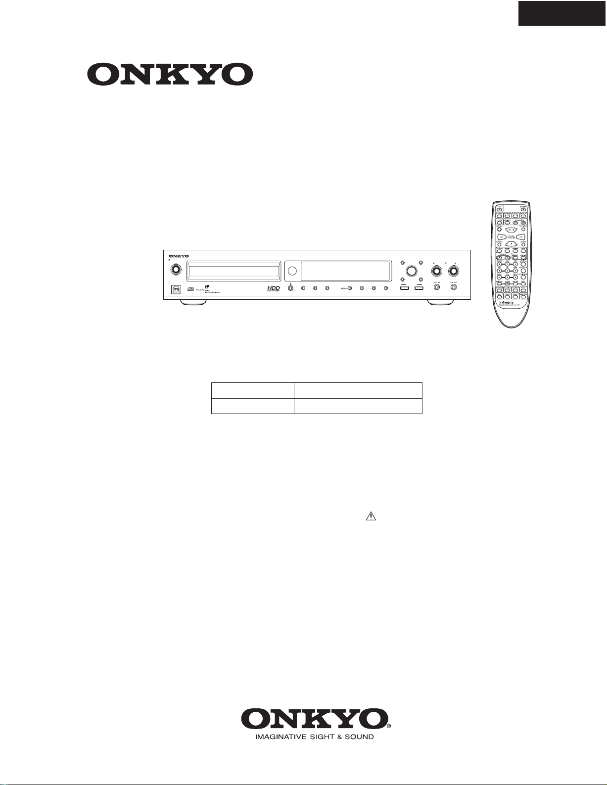
Hard Disk Music Library
MODEL MB-S1
DISPLAY CD DUBBINGTEXT HDD REC REC MODE
FAVORITE IT
EXTERNAL INPUT
PLAY MODE
MENU/EXIT
MULTI JOG
PUSH TO ENTER
OPERATION
C D HDD
EDIT/CLEAR
NOYES
PLAY LIST
HARD DISK MUSIC LIBRARY
STOP PLAY PAUSE
/
MB-S
MB-S1
Ref. No. 3710
112001
1
Main microprocessor version
01X04b
UDD ~#400
UUP ~#400
01X23A
Apply
UDD #401~
UUP #401~
Black, Silver and Titanium models
BUDD
TUUP,SUUT
120V AC, 60Hz
120-240V AC, 50/60Hz
SAFETY-RELATED COMPONENT
WARNING!!
COMPONENTS IDENTIFIED BY MARK ON THE
SCHEMATIC DIAGRAM AND IN THE PARTS LIST ARE
CRITICAL FOR RISK OF FIRE AND ELECTRIC SHOCK.
REPLACE THESE COMPONENTS WITH ONKYO
PARTS WHOSE PART NUMBERS APPEAR AS SHOWN
IN THIS MANUAL.
MAKE LEAKAGE-CURRENT OR RESISTANCE
MEASUREMENTS TO DETERMINE THAT EXPOSED
PARTS ARE ACCEPTABLY INSULATED FROM THE
SUPPLY CIRCUIT BEFORE RETURNING THE
APPLIANCE TO THE CUSTOMER.
Page 2

Specifications
CD-ROM Drive Unit ATA Packet Interface (specified in SFF-8020). (E-IDE)
Hard Disk Drive Unit AT Attachment 5 (ATA-5)
D/A Converter Single bit (Crystal CS4341, 24bit/96kHz)
A/D Converter Single bit (Crystal CS53L32A, 24bit/96kHz)
Connections 2 Analog Output (stereo)
Frequency Response 5Hz - 20 kHz
Playback Harmonic distortion 0.007% (at 1kHz, 0dB)
Playback Dynamic range 90 dB
Playback Signal to noise ratio 90 dB
Recording Harmonic distortion LPCM: 0.007% (at 1kHz, 0dB), MP3: 0.018% (at 1kHz, 0dB)
Recording Dynamic range 90dB
Recording Signal to Noise ratio 90dB
Channel Separation 90dB (playback)
Wow and Flutter Below threshold of measurability
Output Level 2.0 volts r.m.s.
Power Supply Rating & AC120V, 60Hz, 27W
Power Consumption
Dimension (W.H.D,) 435 x 81 x 359 (17-1/8" x 3-3/16" x 14-1/8")
Weight 5.0kg, 11.0 lbs
MB-S1
Industry Standard 3.5" Half Height Form Factor.
Industry Standard 5.25" Half Height Form Factor.
40GB
1 Analog Input (stereo)
2 Digital Input (optical)/(coaxial)
1 Digital Output (optical) (with Audio CD Playback only)
1 USB (Type B)
1 RS-232C (Dsub-9pin)
Specifications and features are subject to change without notice.
Page 3
MB-S1
SERVICE NOTE
1. Replacing the fuses
This symbol located near the fuses indicates that the fuse used is
fast operating type. For continued protection against fire hazard, replace with same type fuse. For fuse rating refer to the marking adjacent to the symbol.
Ce symbole indique que le fusible utlise est a rapide. Pour une protection permanente, n'untiliser que fusibles de meme type. Ce darnier est la qu le present symbol est appse.
CIRCUIT NO. PART NO. DESCRIPTION
F9001 252160 FUSE, 2.5A-UL/T-237 <D>
252076 FUSE, 3.15A-SE-EAK <T,P>
Note: <D>: 120V model only
<P>: European model only
<T>: Asian model only
2. Safety-check out (Only U.S.A. model)
After correcting the original service problem, perform the following
safety check before releasing the set to the customer. Connect the insulating-resistance tester between the plug of power supply cord and
screw on the back panel.
Specifications: 3.3Mohm+/-10% at 500V.
If one of the messages shown below appears
"(Undefined)"
There is no text data or undefined name in the current track.
"Clock Adjust"
The clock of this unit has not been set.
"Copy Protect"
An attempt was made to record copyright-protected material.
"Group Full"
An attempt was made to record more than 999 groups.
"HDD Check ..."
System error occurred. Wait for a while.
"HDD Check 999"
System error occurred. Do not operate the MB-S1 until the count
down is over.
"HDD Media Full"
The HDD is full.
"HDD Only"
This function is only available with HDD mode.
"HDD Track Full"
The number of tracks has reached the limit for input to the HDD.
"New Full "
An attempt was made to enter a new group that exceeds the
maximum group capacity.
LASER W ARNING LABEL
The labels shown below are affixed.
Class 1 label
"CLASS 1 LASER
PRODUCT"
Printed on rear panel
Digital controller board & Firmware are developed
and provided by QPICT, Inc.
LUOKAN 1
LASERLAITE
KLASS 1
LASER APPARAT
"No Disc"
There is no disc in the MB-S1.
"No Favorite"
There are no tracks that have a "favorite it" marking.
"No Genre"
There are no tracks that have a genre.
"No Group"
There is no group data in the HDD.
"No Playlist"
There are no play lists.
"No Track"
There are no tracks in the group; or an appropriate track was not
found.
"Not Audio-CD"
The CD data format is not PCM or MP3.
"Not Available in this Source"
Will not work with the current input source.
"Not Available MP3CD"
The Rec Mode cannot be selected with CDs containing MP3 data.
"P.List Full"
An attempt was made to enter more than 100 tracks in the playlist.
"System Err...Please Power Off & On"
System error occurred. Press the STANDBY/ON button.
"Track Full"
An attempt was made to record more than 255 tracks.
Page 4
MICROPROCESSOR TERMINAL DESCRIPTION
Q7502: MPD780232GC-052-8BT
FUNCTION I/O LOGIC INIT ACTIVE SLEEP P-OFFDESCRIPTIONPIN NO.
1 Vdd1 - - + 5V power supply - - - 2 Vss1 - - GND - - - 3 X2 - - Main clock (5MHz) input terminal - - - 4 X1 - - Main clock (5MHz) input terminal - - - 5 GND - - GND - - - 6 RESET - - microprocessor reset terminal - - - 7 SUBCL/SCK I L Main microprocessor communication and a flash write-in clock input combination terminal Z Z Z Z
8 SUBDI/SDI I P Main microprocessor communication and a flash write-in data input combination terminal Z Z Z Z
9 SUBDO/SDO O P Main microprocessor communication and a flash write-in data output combination terminal L * L L
10 SUBRDY O H The data ready output terminal for communication with a main microprocessor L * L L
11 NC O No use
12 PHOTO I H Photography mode
13 SSCBJ I L SSC rotary encoder pulse input terminal Z Z Z Z
14 SSCAJ I H SSC rotary encoder pulse input terminal Z Z Z Z
15 ~IRMZ I L "Remote control 1 (ZONE2) signal input terminal Active""L"" " Z Z Z Z
16 FAVORITE O FAVORITE Light Emitting Diode output terminal
17 STBYLED O STANDBY/RECEIVED output terminal
18 GND - - The GND terminal of a A/D converter - - - 19-22 K3-K0 I A Main part key input terminal - - - 23 Vss0 - - GND - - - 24 +5V - - The power supply terminal of a A/D converter and +5V are impressed - - - 25 Vdd0 - - + 5V power supply - - - 26 ~SYSIN I L System bath input terminal Z Z Z Z
27 ~SYSOUT O L System bath output terminal H * L Z
28-54 P35-P9 O H Fluorescence display pipe segment output terminal L * L L
55-58 P8-P5 - - Fluorescence display pipe segment output terminal - - - 59 Vdd2 - - + 5V power supply - - - 60 Vload - - The pull down resistance connection terminal of a FIP controller - - - 61-64 P4-P1 - - Fluorescence display tube segment output terminal - - - 65-80 16G-1G - - Fluorescence display tube output terminal
MB-S1
MB-S1
Page 5

MICROPROCESSOR TERMINAL DESCRIPTION
Q7004: MPD70F3033AYGC-8EU
PIN NO. FUNCTION I/O LOGIC DESCRIPTION
1 SO2 O uPD780232(FL TUBE) Synchronous serial output terminal
2 ~SCK2 I/O uPD780232(FL TUBE) Synchronous serial CLK terminal
3 RXD1 I RS-232C(PHAST) input terminal
4 TXD1 O RS-232C(PHAST) output terminal
5 ~WP/ACC O MBM29DL (flash ROM) write-protection / acceleration terminal
6 EVDD - An input-and-output port and positive power supply supply for combination functional terminals
7 EVSS - An input-and-output port and grand potential for combination functional terminals
8 RY/~BY I A MBM29DL (flash ROM) ready / busy terminal
9 MUTE O H Muting ON/OFF terminal
10 SUBMRST O L MB89580 (USB microcomputer) reset terminal (Up (S))
11 FLMRST O L uPD780232 (FL microcomputer) reset terminal (Up (S))
12 USBHRST O L uPD72012 (USB hub tip) reset terminal (Up (S))
13 USBD+ O H USB D+ control terminal (being high pull-up)
14-16 A13-A15 O Address bus 13-15
17 CIRON/OFF O H Circuit power supply ON/OFF
18 IC/VPP - Internal connection (it connects with VSS)
19-30 A1-A12 O Address bus 5-12, 1-4
31 ~RESET I System reset input
"32,33" "XT1,XT2" I Oscillation connection for sub clocks
34 REGC - Regulator output stable capacity connection
"35,36" "X2,X1" I Oscillation connection for main clocks
37 VSS - Ground
38 VDD - Positive power supply terminal
39 CLKOUT O Internal system clock output
40 ~WRL O L The low rank data light strobe signal terminal of the 16 bit data bus of external
41 ~UBEN O L The higher rank byte enable signal output terminal of the 16 bit data bus of external
42 ~WRH O L The higher rank data light strobe signal terminal of the 16 bit data bus of external
43 ~RD O L The lead strobe signal terminal of the 16 bit data bus of external
44 ASTB O The latch strobe signal output terminal of an external address bus
45 CDLED O H CD LED/Program WR Start
46 HDDLED O H HDD LED/Program WR Start
47-54 D0-D7 I/O Data bus 0-7
55 BVDD - A bus interface and the positive power supply terminal for combination ports
56 BVSS - A bus interface and the grand terminal for combination ports
57-64 D8-D15 I/O Data bus 8-15
65-70 A16-A21 I/O Address bus 16-21
71 AVDD - A A/D converter and the analog positive power supply supply terminal for combination ports
72 AVSS - A A/D converter and the grand terminal for combination ports
73 AVREF - The standard voltage supply terminal for A/D converters
74 (intact) (Up (H))
75 PRVSW1 I Destination distinction switch 1 (temporary)
76 PRVSW2 I Destination distinction switch 2 (temporary)
77 SW1 I Model distinction switch (L:MB-S1 H:HDR -1)
78 SW2 I L General-purpose switch 2 (main program forcible download switch)
79 SW3 I L General-purpose switch 3 (for an external ROM/RAM check)
80-85 (intact) (Up (H))
86 NMI I "The terminal for power failure detection (it will input, by the time it will fall completely, if voltage begins to fall) "
87 FROMA0 O (intact)
88 D_MUTE O Digital output muting terminal (Up (H))
89 FLRDY I H FL microcomputer data ready input terminal
90 ELVOL1 Electronic volume control terminal 1
91 ELVOL2 Electronic volume control terminal 2
92 ELVOL3 Electronic volume control terminal 3
93 GAIN_CTL O GAIN CTL port
94 SDA0 I2 C-bus terminal for QPICT board connection (DATA LINE) (Up (H))
95 QPINT O L Interrupt QPICT board signal terminal
96 SCL0 I2 C-bus terminal for QPICT board connection (CLK LINE) (Up (H))
97 RXD0 MB89580 (USB sub microcomputer) asynchronous serial input terminal
98 TXD0 MB89580 (USB sub microcomputer) asynchronous serial output terminal
99 QPRST O L QPICT reset signal terminal
100 SI2 uPD780232 (FL microcomputer) synchronous serial input terminal
MB-S1
Page 6

The test menu operation method - 1
MB-S1
<How to a test menu (level 2) to enter>
1. Change unit into a standby mode.
2. Push the DISPLAY key and the STOP key simultaneously.
-> It is displayed on FL tube as "TEST MODE", and will be in
an all-points light state in about 1 second (test mode level 1
state).
3. Push the CD key and the HDD key.
-> It is displayed on FL tube as "SYSTEM INIT."
It shifts to test mode level 2 state above.
<How to slip out of a test menu (level 2)>
When menus, such as "SYSTEM INIT", are displayed, the
DISPLAY key and the STOP key are pushed simultaneously.
-> It is displayed as "NORMAL MODE" and returns to a
standby state.
<Test menu outline>
SYSTEM INIT:
Initialization of a flash ROM and initialization of HDD are
performed.
DOWNLOAD START:
It shifts to the software rewriting mode of a main program.
FLASH REBUILD:
The information currently recorded on HDD is reconstructed on
a flash ROM.
KEY FUNCTION:
A key function is displayed (with no necessity of using it at the
time of a maintenance).
VERSION:
The version of each program is displayed.
The above-mentioned menu is displayed by turning JOG after test
mode shift.
The selected function is performed when JOG is pushed.
<SYSTEM INIT functional details>
[Method]
1. Choose a menu as "SYSTEM INIT" and push JOG.
2. The message of a check is displayed on FL pipe as "Really?."
Please push the YES key, when you perform. Please push the
NO key, when you cancel.
3. It is automatic in order of "flash initialization ->HDD
initialization",
4. "INIT COMPLETE! If "is displayed, it will be completion of
operation.
[Notes]
- if this function is performed, the music data currently recorded
on all HDD and the inputted tag data will be disappeared and
lost. Be fully careful of handling.
- When HDD is exchanged for a new one, please be sure to
perform initialization of HDD and a flash ROM using this
function.
An incorrect operation will be caused if equipment is used
without performing this function.
- When the power supply of equipment falls by a certain reason
while performing this function, please perform again.
An incorrect operation will be caused if equipment is used in the
state where it is initialized halfway.
[The use pattern assumed]
- When HDD is exchanged
<DOWNLOAD START functional details>
[Methode]
1. Choose a menu as "DOWNLOAD START" and push JOG.
2. The message of a check is displayed on FL pipe as "Really?."
Please push the YES key, when you perform. Please push the
NO key, when you cancel.
3. The display of FL tube disappears and the CD button and the
HDD button of equipment light up after a while.
4. Connect a USB cable between unit and PC and download by
starting farm download software (bluefire).
[Notes]
- It becomes impossible to use unit, once it performs this function
until it next finishes writing in software.
Since it does not usually return to processing even if it takes out
and inserts AC plug, be careful of handling enough.
- Before the CD button and the HDD button light up, even if it
starts farm download software (bluefire), an error is displayed
and software may not start.
Please restart software again after waiting to switch on the light.
<FLASH REBUILD functional details>
[Methode]
1. Choose a menu as "FLASH REBUILD" and push JOG.
2. The message of a check is displayed on FL pipe as "Really?."
Please push the YES key, when you perform. Please push the
NO key, when you cancel.
3. Flash ROM initialization -> perform data reconstruction
processing automatically.
4. "REBUILD OK! If "is displayed, it will be completion of
operation.
[Notes]
- If this function is performed, since it is unrestorable, please
understand beforehand the tag information inputted into the
music data currently recorded in PCM form among the tag
information inputted
(Since the domain which stores tag information does not exist in
the PCM file currently recorded on HDD on the relation of a file
system)
- When the power supply of equipment falls by a certain reason
while performing this function, please perform again.
An incorrect operation will be caused if equipment is used in the
state where it is reconstructed halfway.
- When the music data currently recorded on HDD exists in large
quantities, this thing has time in processing.
- Please do not perform this function to HDD which has not
performed SYSTEM INIT processing once.
It is in the middle of of operation, and may hang-up.
[The use pattern assumed]
- When substrate exchange is performed
Page 7

The test menu operation method - 2
<VERSION functional details>
[Real whereabouts method]
1. Combine a menu with "VERSION" and push JOG.
2. The version of each farm is displayed. A display can be changed
by turning JOG.
The contents displayed are as follows.
- Main ....
Soft version number currently recorded on the external flash
ROM (whole charge of operation)
- Boot ....
Soft version number currently recorded in CPU (V850) of a
main board (starting processing charge)
- Disp ....
Soft version number currently recorded on CPU of a display
board (display processing charge)
- USB ....
Soft version number currently recorded in CPU (MB89) of a
main board (USB communication charge)
- The soft version number currently recorded on the QP-B....
QPICT board (device control charge)
Please push the MENU/EXIT key, when you escape from this
mode.
[Notes]
- When you check the version of QPICT software (QP-B), please
reboot unit.
Please perform this function again and check a version, after
performing "POWER ON-> standby state ->OFF."
MB-S1
Page 8
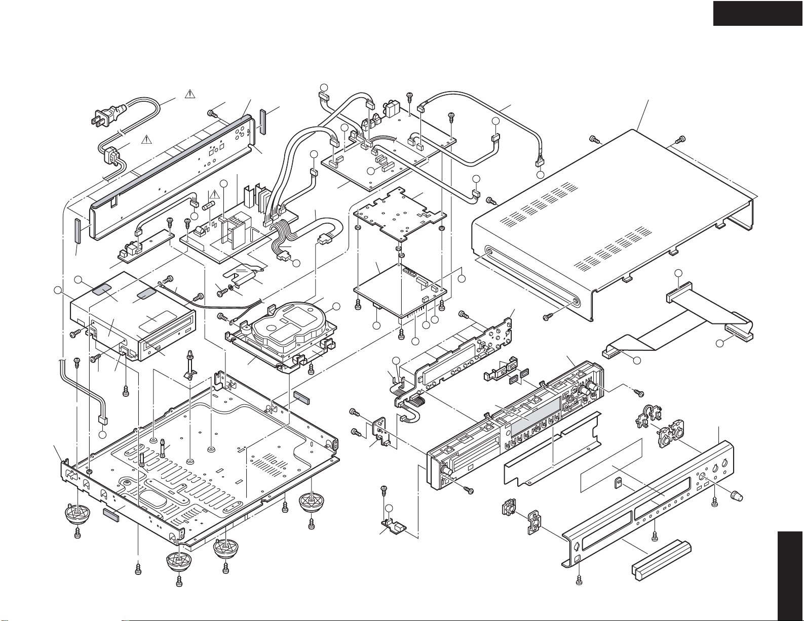
EXPLODED VIEW
E8
A20
G
Z6
A1
A16 A17
A37
A36
U2
H
A18
Z3
Z6
A27
A24
Z5
K
A25
A22
A36
Z2
A37
Z6
A21
E7
E5
A36
F
Z6
A23
A16
F9001
Z5
Z4
A34
K
A36
U5
A24
A16
A38
A39
A15
A30
A20
A37
E2
G
A17
A36
A
E1
Z4
B
U1
Z1
A28
A16
MB-S1
A37
E4
A37
D
A34<D>
A35<T,P>
C
E
U4
A34<D>
A35<T,P>
A9
F
L
U7
A26
A26
B
A37
A37
A
C
I
A26
A26
U8
J
A37
D
A37
L
E6
A34<D>
A35<T,P>
A5
A19
A31
A37
U6
A29
A37
E
A37
A12
A13
U3
A11
A4
H
A34
A32
A37
E3
A10
I
A14
A34<D>
A35<T,P>
A34
J
A2
A8
MB-S1
A33
A34
Page 9

EXPLODED VIEWS - PARTS LIST
MB-S1
No. Description Part number
U1 PC BOARD AS,NAAR-7346-1A 1W225546-1A
U2 PC BOARD AS,NAETC-7347-1A 1W225547-1A
U3 PC BOARD AS,NAETC-7348-1A 1W225548-1A
U4 PC BOARD AS,NADIS-7349-1A 1W225549-1A
U5 PC BOARD AS,NAPS-7350-1A 1W225564-1A <D>
PC BOARD AS,NAPS-7350-1B 1W225564-1B <T,P>
U6 PC BOARD AS,NASW-7351-1A 1W225551-1A
U7 PC BOARD AS,NAETC-7359-1A 1W225564-1A
U8 PC BOARD AS,NQP310OD 24150024
E1 SOCKET AS,NSAS-8P0963 2009990694
E2 SOCKET AS,NSAS-8P0964 2009990695
E3 SOCKET AS,NSAS-120P0962 2009990693
E4 SOCKET AS,NSAS-8P0983 2009990706
E5 CRIMP AS,SRA-STRIP(300) 20799132
E6 CLIP,CS-1U 27255004
E7 AC CORD,AS-UC-2#18 253279HDK <D>
AC CORD,AS-CEE or 253193HIT or <T,P>
AC CORD,AS-CEE 253313HRK <T,P>
E8 BUSHING,S-RELIEF #2271 27300750
F9001 FUSE,2.5A-UL/T-237 252160 <D>
FUSE,3.15A-SE-EAK 252076 <T,P>
A1 CHASSIS 27100407A
A2 F PANEL 27212357 <D>
27212355 <T>
27212356 <P>
A3 BADGE 28135244Y <D>
A4 CLEAR PLT 28191950 <D>
28191946 <T>
28191947 <P>
A5 F BRACKET 27111255 <D>
27111253 <T>
27111254 <P>
A8 KNOB(AMCS) 28325930 <D>
28325967 <T>
28325968 <P>
A9 FACET(HDD,CD) 28198941
A10 FACET(STOP) 28198928
A11 FACET(STANDBY) 28198930
A12 FACET(FAVORITE) 28198940
A13 GUIDE(STANDBY) 27268049 <D>
27268047 <T>
27268048 <P>
A14 GUIDE(STOP) 27268053 <D>
27268057 <T>
27268058 <P>
A15 REAR PANEL 27122920 <D>
27122919 <T,P>
A16 BOTTOM LEG(AS) 27175388
A17 CUSHION(SHLD) 28141490
No. Description Part number
A18 CUSHION 28141491
A19 CUSHION 28141486
A20 CUSHION 28141467
A21 HOLDER,KGLS-18RF 27190657
A22 HOLDER,KGPS-18RF 27190926
A23 HOLDER,KGLS-18S 27190470
A24 HOLDER(CD) 27191160A
A25 SPACER 27270429
A26 SPACER,PVC T1.0 27270427
A27 ISO PLT(CD) 28175281
A28 ISO PLT(HDD) 28175282
A29 ISO PLT(CU) 28175280
A30 ISO PLT(HS) 28175283
A31 B PLATE 28133400 <D>
A32 COVER 28184821 <D>
28184820 <T,P>
A33 DOOR 28148500 <D>
28148498 <T>
28148499 <P>
A34 SCREW,3TTB+8B(BC) 838430088
A35 SCREW,3TTB+8B(UN) 838930088 <T,P>
A36 SCREW,3TTW+8B(BC) 831430088
A37 SCREW,3TTB+8B 838130088
A38 SP WASHER,SE-3(BC) 871430
A39 TAPE(CROSS-8U) 29110082
Z1 Hard Disk Drive,MPG3204AT-EF 24842001
Z2 CD-ROM MECHA,CR-594-C 24800049
Z3 LABEL 29362285
Z4 SCREW,No.6-32*1/4UNC 801603
Z5 SCREW,3P+10FN(BC) 82143010
Z6 SCREW,3P+6FN(BC) 82143006
Note: <D>: 120V model only
<P>: European model only
<T>: Asian model only
SAFETY-RELATED COMPONENT WARNING!!
COMPONENTS IDENTIFIED BY MARK ARE CRITICAL FOR
RISK OF FIRE AND ELECTRIC SHOCK.
REPLACE THESE COMPONENTS WITH ONKYO PARTS
WHOSE PART NUMBERS APPEAR AS SHOWN IN THIS
MANUAL.
MB-S1
Page 10
MB-S1
330
P
A
BCD
SCHEMATIC DIAGRAM (NAAR-7346) -1
1
2
3
4
LEVEL_LCH
DAC_GND DAC_GND IIS_LRCK
LEVEL_RCH
LEVEL_CTRL
J2J1
A+B
AGND
A-B
EV5V D+5VA
P4901
FROM POWER
AUDIO_POWER D+5VA D+5VA
R4319
L_CTRL_C LEVEL_CTRL
SBY_M_C STANDBY_MUTE
TO CPU CIRCUIT(2/3)
47
R4304
47
R4305
47
R4306
47
R4307
47
R4308
47
R4309
47
R4310
47
R4311
47
P4302
R4312
47
TO_JP12_QPICT_U003
R4313
47
R4314
47
R4315
47
R4316
47
R4317
47
R3001
47
R3002
47
R3003
47
P3001
TO_JP17_QPICT_U003
R3004
47
DGND
MUTE_LINE MUTE_LINE
SPDIF_+5V
SPDIF_IN1
SPDIF_IN2
SPDIF_GND
DSP_SPDIF_OUT
R4511
0
-B
6
R4507
0
5
R4508
0
3
2
+B
R4512
SPI_CS0_
SPI_CS2_
SPI_CLK
SPI_DATA_TO_DEV
ADC_RESET_
DAC_RESET_
AUDIO_CLK
IIS_LRCK
IIS_CLK
IIS_D_ADC
IIS_D_FROM_DSP
IIC_SDA
IIC_SCL
DGND
Q4501
NJM4580M
4
7
1
Q4501
8
NJM4580M
0
R4513
3.3K
C4507
C4508
R4514
3.3K
47/16
47/16
10
R4548
AGND
A-B
A-B
A+B
10
R4556 10
R4555
47/16
C4538
C4540
R4547
A+B
R4901
0
R4903
0
AGND
47/16
R4515
R4516
10
C4905
C4910
104Z
C4539
C4551
47/16
18K
18K
C4552
47/16
L4501
47/16
47/16
R4538
R4540
C4541
C4509
104Z
C4510
R4551
100/6.3
10
R4520
C4511
R4552
104Z
C4512
100/6.3
BLM21P221SG
VMID_L
STANDBY_MUTE L_MUTE L_MUTE
5
VIN
104Z
C4906
Q4901
CTRL1GND2NB
R4902
1K
5
VIN
104Z
C4911
Q4902
CTRL1GND2NB
R4904
1K
R4539
L4504
47
BK1608HS102
22K
104Z
C4542
C4543
47/16
22K
104Z
47/16
C4545
C4544
104Z
H07
100K
Q4502 DS1801E
W1
VMID_R
8
100K
VMID_R
VMID_L
4
VOUT
3
C4907
4
VOUT
3
C4912
NJM4580M
8
+B
2
3
5
6
-B
4
NJM4580M
R4518
4
L0 6L19
W05
ZCEN
H110
AGND11
SPI_DATA_TO_DEV
D+5VA
C4908
NJM2370U05
1/50
D+3VA
C4913
NJM2370U33
1/50
D+5VA
Q4505
R4541
3.3
1
R4542
7
3.3
Q4505
47/16
47/16
0
3
RST
D12
CLK
13 COUT2
SPI_CLK
C4909
C4914
VMID_R
VMID_L
GND1
VCC14
104Z
R4605
104Z
R4606
0
0
IIC_SCL
101
C4524
R4601
R4602
102
C4525
1M
680K
102
C4526
R4604
0
IIC_SDA
SCL/CCLK/CHSEL10
AFLTR11
C4527
R4527
0
NJM4580M
4
Q4503
C4513
47/16
-B
6
R4523
5
0
150K
R4521
150K
R4522
R4524
3
0
2
+B
8
NJM4580M
47/16
C4514
DGND
DAC_GND
SPI_CS0_
Q4503
R4528
0
D+3VA D+3VA
A+B A+B
AGND AGND
A-B A-B
DGND DGND
D4601
EV5V
C4601
47/16
C4602
D4602
STANDBY_MUTE
1SS352
D4603
1SS352
7
1
1SS352
104Z
C4603
R4529
3.3K
C4519
47/16
C4520
10
R4549
A+B
AGND
C4604
R4607
470/6.3
Q4602
Q4603
M51943BSL
I
R4530
3.3K
47/16
10
R4550
A-B
0.1/50
RN2403
47K
RN1404
R4608
10K
O
G
C4521
0.47/50
R4553
C4522
0.47/50
Q4601
R4603
R4609
5.1K
R4554
10K
47
5.1K
101
C4523
SDA/CDIN/DIF9
AFLTL12
22/16
IIS_LRCK
LRCK7
AD0/CS/DIV8
FILT+13
AIN_R214
IIS_D_ADC
VA5
GND6
CS53L32A
Q4504
AIN_L215
REF_GND16
104Z
C4529
R4007
IIS_CLK
SCLK3
SDOUT4
AIN_L118
AIN_R117
104Z
C4530
0
AUDIO_CLK
ADC_RESET_
VL 1
MCLK2
VQ
RST
19
20
R4535
10K
C4531
22/16
L4502
BLM21P221SG
D+3VD
C4533 104Z
C4534
100/6.3
R4536
R4537
22
DAC_RESET_
IIS_D_FROM_DS
C4536
470/6.3
C4537
104Z
10
L4503
BLM21P221SG
IIS_CLK
AUDIO_CLK
SPI_CLK
SPI_DATA_TO_DEV
SPI_CS2_
120
47K
R4033
R4002
C4001
High: NORMA
330
120
R4003
C4002
5
Page 11

MB-S1
330
K
V
A
BCD
SCHEMATIC DIAGRAM (NAAR-7346) -2
1
NAAR-7346
C4023
R4027
820
472
8
+B
C4003
470/6.3
ET_
RST
MUTEC16
1
_DSP
SDATA2
AOUTA15
VA14
AGND13
AOUTB12
VQ
FILT+ 9
4.7K
10
C9
GND8
B10
VEE7
R4006
C4005
C4007
22/16
C4009
0
A11
X0 12
Q4506
TC4053BFT
EN6
Z05
22
22/16
104Z
13
X1
Z4
Y15Y02
X14
Z1
3
L4001
BLM21P221SG
A+B
AGND
A-B
DGND
L_MUTE
VCC16
Y11
47/16
47/16
C4546
C4549
R4557
10
82K
27K
27K
82K
R4558
10
R4505
R4545
R4546
R4506
C4501
22/50
C4502
22/50
100K
100K
101
R4503
101
R4504
R4501
SCLK3
Q4001
LRCK4
LK
120
R4003
330
C4002
2
3
RMAL Low: -12dB
CS4341
5
MCLK
REF_GND11SCL/CCLK6
SDA/CDIN7
AD0/CS8
10K
R4004
DAC_GND
R4008
DGND
LEVEL_LCH OUT1_RCH
R4544
Q4507
RN1404
LEVEL_CTRL
DAC_GND
LEVEL_RCH
100
C4547
C4548
R4502
100
0
R4519
R4031
R4032
A+B
IN_LCH
DAC_GND
IN_RCH
A-B
C4017
R4021
47/16
C4018
47/16
R4017
R4018
R4019
1.8K
100K
100K
R4020
1.8K
2.2K
C4019
C4020
R4022
2.2K
222
DAC_GND
222
0
0
R4023
1.8K
R4024
1.8K
C4021
C4022
C4024
472
102
102
R4025
R4026
2
3
1K
1K
5
6
R4028
Q4003
820
1
Q4003
NJM4580M
NJM4580M
7
-B
4
R4010
A-B
C4027
C4028
10
470/16
470/16
R4009
AGND
A+B
LO
SPDIF_GND
E4302
RO
E4304 E4303
E4305E4306
10
0
0
C4105
22/50
C4106
22/50
R4119
R4105
R4106
100K
100K
L_MUTE
R4107
220
R4113
4.7K
Q4103
HN1C03F
R4114
4.7K
Q4104
HN1C03F
R4108
220
2
5
R4120
C4301
104Z
R4318
0
6
1
4
3
E4301
GROUND
R4109
220
R4115
4.7K
Q4103
HN1C03F
R4116
4.7K
Q4104
HN1C03F
R4110
220
5
2
E4307
R4111
47
3
4
1
6
R4112
47
C4107
101
101
C4108
0
R4117
IN_LCH
DAC_GND
IN_RCH
OUT1_LCH
DAC_GND
P4101
ANALOG_IN_LCH
ANALOG_IN_RCH
ANALOG_OUT1_LCH
ANALOG_OUT1_RCH
DAC_GND
L3001
BLM21P221SG
SPDIF_+5V
SPDIF_IN1
4
74HCU04AF
Q3001
56
SPDIF_IN2
DSP_SPDIF_OUT
SPDIF_GND
9
D_MUTE
Q3001
5
74HCU04AF
C3001
100/6.3
8
14
GND7
VCC
Q3001
10
74HCU04AF
R3005
Q3001
47
74HCU04aF
104Z
C3002
R3011
100K
4
3
R3010
Q3001
47
74HCU04AF
Q3004
8
1
VCC
27
63
5
4
GND
TC7W00FK
104Z
C3012
R3006
11
Q3001
74HCU04AF
C3006 470
R3012 10K
2
1
Q3001
74HCU04AF
L3003
BLM21P221SG
1312
C3007
104Z
C3009
100K
R3008
R3007
C3003
104Z
150K
R3009
C3004
L3002
BK1608LL241
R3013
C3010
100/6.3
100/6.3
150
104Z
C3005
C3008
101
104Z
R3014
150
R3015
100
OPTICAL_DIGITAL_IN
3
Q3002
2
GP1FA550RZ
1
P3002
COAXIAL_DIGITAL_IN
OPTICAL_DIGITAL_OUT
3
Q3003
2
GP1FA550TZ
1
Page 12

MB-S1
9
A
BCD
SCHEMATIC DIAGRAM (NAAR-7346) -3
1
2
3
P7001
L_CTRL_C GAIN_CTRL CDLED
SBY_M_C
D_MUTE
DGND
4
P7003
5
A16 A17
A151A1648
MA15 BYTE MWP/ACC
MA14
MA13 D15 MA14 A13
MA12 D7 MA15 A14
MA11 D14 MA5 A15 F+ FL+
MA10 D6 MA6 A5
MA9 D13 MA7 A6
A21 D5 MA8 A7
WR
FLRRST 3.3V
MWP/ACC D3
FRRY/BY D10
A19 D2 F- FLFA18 D9 MA9 FL+ FLF+
MA8 D1 MA10 A9 -VDISP FL-V
MA7 D8 MA11 A10 E5V FL5V
MA6 D0 MA12
MA5 RD MA1 A12 FLSUBRDY FL_RST
MA4
MA3 SELFRAM MA3 A2 SO2 SUB_DI
MA2 MA1 MA4
MA15 A16 FMA14 F+
MA13
MA12 D15
MA11 D7
MA10 D14 WGND WGND FLGND
MA9
MA8 D13 SDO
WR D4 WSDI WSDI FL5V
UB
LB D10
MA7 D1
MA6 D8
MA5 D0 E5V B5V
MA4 RD
MA3
MA2 SELSRAM
MA1 A17
F+ RST
F-
-VDISP
L7001
BLM21P221SG
TO POWER BOARD
R7001
47
104Z
C7001
R7072
47
R7005
47
R7100
0
GND
R7010
1K
R7007
QPINT SO0
470
R7008
SCL0 SCK0
R7006
SDA0 SI0
QPICT_RST
TO QPICT BOARD
R7015
1K
GND
BYTE
A142
VSS2
A133
A124
DQ15/A-1 45
A115
A106
DQ1443
A97
A88
DQ1341
A199
10
NC1
DQ1239
11
WE
RESET12
NC213
DQ1136
WP/ACC
14
RY/BY15
DQ1034
A1816
A1717
A718
A619
A520
Q7001
A421
MBM29DL163BE
VSS1 27
A322
A223
A151A1648
A142
A133
A124
IO16 45
A115
A106
IO15 43
A97
A88
IO14 41
9
NC1
NC2
10
IO13 39
WE
11
CE212
IC13
IO12 36
14
UB
LB
15
IO11 34
16
NC3
Q7002 MPD442012L
NC4
IO10 32
17
A718
A619
A520
A421
A322
GND127
A223
E5V
CIRON/OFF SELFRAM RD
O
I
G
Q7003
SI-3033LUS
100/6.3
C7002
GND
PHOTO
S7028
CIRON/OFF HDDLED
ELVOL1
ELVOL2 DSTB
ELVOL3 R/_W
MUTE UB
3.3V RXD0 A3
Q7011
4.7K
4.7K
R7061
R7060
47
Q7014
47
R7009
470
4.7K
R7063
R7021
47
0
46
DQ7 44
DQ6 42
DQ5 40
D12
D4
DQ4 38
VCC 37
D11 F-
DQ3 35
DQ2 33
32
DQ9
DQ1 31
DQ8 30
DQ0 29
OE
28
CE
26
A0 25A124
NC5 47
GND2
46
IO8 44
IO7 42
IO6 40
IO5 38
37
VCC
IO4 35
IO3 33
IO2 31
IO9
30
IO1 29
28
OE
CE1
26
A0 25A124
B5V WR
3.3V
104Z
100/6.3
C7005
C7004
R7016
S7029
DOWNLOAD
4.7K
R7014
R7012
4.7K
R7035
3.3V
CIRON/OFF FLSUBRDY
GAIN_CTRL
MUTE
D_MUTE SCK0 A4
QPRST QPRST A1
2SK3019
2SK3019
4.7K
R7062
104Z
C7006
GND
3.3V CDLED FLCDLED
C7009
GND
D6 FLRRST WSDO WSDO SDI
D5 W5V W5V SCK
D12 RST WSCK WSCK FL_RST
D11 WRST
D3
D2
D9
4.7K
C7010
100/6.3
R7018
R7022
4.7K
4.7K
R7019
R7029
R7030
4.7K
4.7K
R7020
R7031
R7032
R7033
R7034
4.7K
R7026
R7036
ELVOL1 E5V
ELVOL2 RY/BY
ELVOL3
SI0
SO0 RST
TXD0 A2
R7105
R7106
SI2
FLSUBRDY
100/6.3
C7008104Z
D7009
CRS08
100
R7115
0.1
104Z
C7045
C7043
R7099
0
R7037
PRVSW1
4.7K
3.3V
GND
104Z
C7011
PRVSW2 D3 E5V USB3.3V
76
77
78
P75/ANI579
P76/ANI680
P77/ANI781
P80/ANI882
P81/ANI983
P82/ANI1084
P83/ANI1185
P00/NMI86
P01/INTP087
P02/INTP188
47
P03/INTP289
47
P04/INTP390
47
P05/INTP4/ADTRG91
47
P06/INTP5/RTPTRG92
47
P07/INTP693
47
P10/SI0/SDA094
47
P11/SO095
47
96
47
97
47
98
47
99
100
C7013
100/6.3
R7107
R7109 10K
10K
P71/ANI1 75
P21/SO21
1K
R7135
SO2
1K
SCK2
AVREF73
P70/ANI0 74
P22/SCK2/SCL12
P23/RXD1/SI33
R713747R7136
R7138
RXD1
SW1 D2
SW2 D1
SW3 D0
4.7K
4.7K
4.7K
4.7K
4.7K
4.7K
PWCUTDT LB
4.7K
R7056
R7077
R7126
R7127
R7089
R7128
R7129
R7130
R7131
R7132
R7133
R7134 1K
104Z
C7012
C7024 104Z
20
NC1VCC
OE
A12
MA13 WP/ACC
10
MA2 A1 SI2 SUB_CL
10
R7058
470
1K
1
R7059
2
3
GND
TC7S32FU
A20
A21
A21
A20
A19
A18
AVDD71
AVSS72
P63/A19 68
P64/A20 69
P65/A21 70
76:P72/ANI2
77:P73/ANI3
78:P74/ANI4
96:P12/SCK0/SCL0
97:P13/SI1/RXD0
98:P14/SO1/TXD0
99:P15/SCK1/ASCK0
100:P20/SI2/SDA1
EVDD6
EVSS7
P24/TXD1/SO34
P25/ASCK1/SCK35
P26/TI2/TO28
47
47
47
R7139
MUTE
RY/BY
WP/ACC
TXD1
19
B1 18
A23
B2 17
A34
B3 16
A45
B4 15
A56
B5 14
A67
B6 13
A78
B7 12
A89
Q7009 TC7MBD3245FK
B8 11GND
C7025
104Z
NC1VCC
20
OE
A12
19
B1 18
A23
B2 17
A34
B3 16
A45
B4 15
A56
B5 14
A67
B6 13
A78
B7 12
A89
Q7010 TC7MBD3245FK
B8 11GND
Q7006
5
VCC
4
C7015
C7018 100/6.3
C7019 104Z
Q7007
5
1
3.3V
VCC
2
4
3
GND
TC7S32FU
Q7008
1
8
VCC
27
63
4
5
GND
TC7W00FK
GND
A17
A16
D15
D14
D13
D12
P60/A16 65
P61/A17 66
P62/A18 67
P54/AD12 61
P55/AD13 62
P56/AD14 63
P57/AD15 64
Q7004
MPD703033AY_MAIN
P27/TI3/TO39
P30/TI0010
P31/TI0111
P32/TI10/SI412
P33/TI11/SO413
P34/TO0/A13/SCK414
P35/TO1/A1415
47
47
47
A13
A14
R7144
R714247R714147R7140
R7143
R7073
USBD+
FLMRST
SUBMRST
USBHRST
R7091
R7068
4.7K
Q7016 2SC2120
330
R7069
C7029
D4
P44/AD4 51
P45/AD5 52
P46/AD6 53
P47/AD7 54
P41/AD1 48
P40/AD0 47
P96/HLDRQ46
P95/HLDAK45
P94/ASTB44
P93/DSTB/RD
P92/R/W/WRH42
P91/UBEN41
P90/LBEN/WRL40
CLKOUT39
VDD38
VSS37
X1 36
X2 35
REGC34
XT2
XT1 32
P103/RTP3/KR3/A822
P104/RTP4/KR4/A923
P105/RTP5/KR5/A1024
P106/RTP6/KR6/A1125
A10
A11
E5V
R7025
4.7K
GND
22/50
104Z
C7035
C7003
100/6.3
50
49
R7049
470
470
R7050
43
C7031
C7032 104Z
C7030
1/50
33
R7043
31
47
30
29
28
27
A12 FRRY/BY
26
SI0
SO0
RST
SCK0
47
R7047 47
R7040 47
R704447R7045
P7006
FOR FLASH WRITER
A8
A11
A3 SCK2 SUB_DO
A4 FLMRST SUB_RDY
104Z
C7016
100/6.3
SELSRAM
104Z
C7020
104Z
C7021
D9D8D7D6D5
D11
D10
56
BVDD55
BVSS
P50/AD8 57
P51/AD9 58
P52/AD10 59
P53/AD11 60
50:P43/AD3
49:P42/AD2
31:_RESET
30:P113/A4
29:P112/A3
28:P111/A2
27:P110/WAIT/A1
26:P107/RTP7/KR7/A12
IC/VPP18
P100/RTP0/KR0/A519
P101/RTP1/KR1/A620
P102/RTP2/KR2/A721
P36/TI4/TO4/A1516
P37/TI5/TO517
A5A6A7A8A9
A15
CIRON/OFF
VPP
10K
C7022 104Z
C7023
100/6.3
NAAR-7346 NADIS-734
1SS352
D7002
104Z
C7027
22/50
22/50
UDZS5.1B
D7001
C7026
P7007
WVPP WVPP FL_VPP
FOR FLASH WRITER
RD
WR R/_W
100/6.3
X7001
C7033
CSTCV16.00MXJOC
22P
C7041
C7034
105
22P
C7042
104Z
VPP
R7046 0
C7028
P7008
TO DISPLAY BOARD
GND
RI SUB_RI
HDDLED FLHDDLED
P7015
FOR FLASH WRITER
WRST
E5V
1
X7002
2
3 4
32.768KHZ
O
G
Q7012
I
M51943BSL
RST
RI
3.3V
Q7025
1
27
DSTB RD
4
GND
TC7W00FK
GND
Q7013
SI-3033LUS
I
O
G
C7046 100/6.3
C7044 104Z
R7039
470
RXD0
TXD0
SUBMRST
104Z
C7014
C7007 100/6.3
Q7005
8Y16
VCC
5G7
A2
A1
GND
Y2
3G1
2
4
470
R7024
8
VCC
63
5
C7039
100/6.3
104Z
C7049
C7048
TC7WT241FU
P7501
FROM CPU BOARD
P7502
FOR FLASH WRITER
104Z
FLGND
C7501
100/6.3
Q7026
1
8
VCC
27
63
WR
5
4
GND
TC7W00FK
10K
R7051
C7050
470
R7048
470
R7027
R7023
104Z
C7502
C7040
100/6.3
1K
104Z
C7052 104Z
R7054
Page 13

MB-S1
A
BCD
SCHEMATIC DIAGRAM (NAAR-7346) -4
NADIS-7349
F+62
1
2
3
Q7026
1
27
4
GND
TC7W00FK
R7051
R7048
R7027
4
F+.61
FLF+
FLF- FLF-
470
470
R7503
D7503
R7511
103Z
4.7/50
C7505
R7501
470
D7501
UDZS5.6B
R7502
220K
C7503
R7507
R7508
R7509
R7510
101
C7504
R7505
R7506
R7502
FLF- FL5V
FLF+ FLGND
FL-V SCK P5
FL5V SDI P6
FLGND SDO P7
FL_RST P8
SUB_CL P9
SUB_DI
SUB_DO P11
SUB_RDY P12
SUB_RI P13
FLHDDLED P14 K0
FLCDLED SSCBJ P15
104Z
C7502
C7501
100/6.3
FLGND K2 P22
SDI
SDO
SCK K2
FL_RST
FL5V
FL_VPP
ZENER_D
C7508
100/6.3
RN2403
104Z
12
R7515
2.7K
R7516
2.7K
Q7501
4
6
2G3G4G5G6G7G8G
80
FIP0
FIP1 79
VDD11
VSS12
X13
X2
IC/VPP5
RESET
P27/SCK17
P26/SI18
P25/SO19
P24/BUSY10
P2311
P22
P21/SO313
P20/SCK314
P00/INTP015
P01/INTP116
P02/T117
AVSS18
ANI319
ANI220
ANI022
ANI1
21
C7510
K1
K0
100/6.3
R7517
47K
4.7/50
C7506
R7512 22K
C7507
R7504
X7501
47
47
CSTCR5.00G
47
470
470
470
470
SSCAJ
IRMZ P17
FAVORITE_LED P18
10K
R7598
STANDBY_LED P19
K3 P21
2.7K
2.7K
R7514
R7513
D7502
1SS352
47K
FIP2 78
VSS023
C7509
104Z
9G
10G
11G
12G
FIP3 77
FIP4 76
FIP5 75
FIP6 74
FIP7 73
FIP8 72
FIP9 71
FIP10 70
FIP11 69
Q7502
MPD780232GC-052-8BT
FIP46/P5632
FIP47/P5731
FIP48/P6030
FIP49/P6129
FIP50/P6228
FIP51/P6327
FIP52/P6426
AVDD24
VDD025
P35
P34
P33
P32
P31
SYSIN
SYSOUT
NASW-7351
150
470
4.7K
R7531
R7535
R7539
D7508 STBY-ON
VCC
10K
SEL2910A-TP6
S7520
P63/DI3 56
P64/DI4 57
P65/DI5 58
Q7015
18:P54/CEX
X1
VSS224
25
23
R7104
0
C7060
POWER_STANDBY
MB_D-
MB_D+
RPVM52
RPVP51
P60/DI0 53
P61/DI1 54
P62/DI2 55
MBM89585BW-115
X7003
6MHZ_HC-49/U
330
C 50
P2131P2230P2329P2428P2527P2626P27
R7028
49
P00 48
P01 47
P02 46
P03
P04
P05
P06
P07
P10
P11
P12
P13
P14
P15
P16
P17
P2032
1.5K
VCC
45
44
43
42
41
40
39
38
37
36
35
34
33
8
RD
63
5
104Z
C7040
470
470
C7050
100/6.3
R7023
104Z
C7052
1K
1
2
3
4
DO7/P47/PWM2/D7
P30/INT0/CLK5
P31/INT16
7
P32/INT2
P33/INT3
8
P34/INT4
9
4.7K
R7054
10
P35/INT5
11
P36/INT6/WEX
12
P37/INT7/RDX
P50/OBF/IBFX/W13
VSS114
15
P51/R
P52/EFX16
101
R7041
C7054
SUBMRST
62
63
64
P40/D0/DO061
P41/D1/DO1
P42/D2/DO2
P43/D3/DO3
MOD020
RST
17
18
19
1K
470
R7057
P66/DI6 59
P67/DI7 60
1:DO4/P44/UCK/D4
2:DO5/P45/UO/D5
3:DO6/P46/U1/PWM1/D6
17:P53/A0/FFX
X022
MOD1
21
330
C7059
Q7510
RN1407
R7074
R7075
PC_+V
10K
4.7K
D7506
RN1407
1K
R7042
STBY-POWER
Q7508
R7076 470
USBHRST
P3457
P3558
P35
P34
13G
14G
15G
FIP12 68
FIP13 67
38:FIP40/P50
FIP44/P5434
FIP45/P5533
P30
P29
P28
2.2K
R7599
101
C7065
R7078 4.7K
P3154
P3255
P3356
P33
P32
P31
P30
P1P2P3
FIP14 66
FIP15 65
FIP16 64
FIP17 63
FIP24/P30 54
FIP25/P31 53
FIP26/P32 52
FIP27/P33 51
FIP28/P34 50
FIP29/P35 49
FIP30/P36 48
FIP31/P37 47
FIP32/P40 46
FIP33/P41 45
39:FIP39/P47
40:FIP38/P46
FIP34/P42 44
FIP35/P43 43
FIP36/P44 42
FIP37/P45 41
FIP41/P5137
FIP42/P5236
FIP43/P5335
38
P27
P26
P25
100/6.3
C7066
1.5K
R7080
PC_D+
PC_DMB_D+
MB_D-
4.7K
R7079
P3053
P29
VLOAD
FIP18 62
VDD2 59
FIP20 58
FIP21 57
FIP22 56
FIP23 55
39
P24
104Z
C7067
Q7503
BJ843GNK
P1033
P1134
P1235
P1336
P1437
P1538
P1639
P1740
P1841
P1942
P2043
P2144
P2245
P2346
P2447
P2548
P2649
P2750
P2851
P2952
P28
P27
P26
P25
P24
P23
P22
P21
P20
P19
P18
P17
P16
P15
P14
P13
1G
16G
100K
100K
R7565
Q7504
RN1407
100/6.3
C7511
4.7K
R7547
IRMZ
SSCBJ
P7503
POWER LED
L7012
BLM21P221SG
PP140PP241PP342PP443PP5
Q7019
D2113
D3014
D3115
DGND416
15K
15K
R7084
R7083
QPICT_-D
QPICT_+D
PC_DPC_D+
PC_+V
R7550
Q7505
RN1407
Q7513
REMSENS
104Z
C7512
4.7K
R7548
3
5
2
6 7
1
4
SSCAJ
STANDBY_LED
39
36
CS435CS5
DVDD338
DVDD4
CLKSEL37
DGND731
DVDD230
AVDD229
AGND228
AGND127
MPD72012-124
CLK/X2 25
D4018
D4119
D5020
D5121
DGND517
15K
15K
15K
15K
R7088
R7087
R7086
R7085
ENTER
S7501
CS334
CS2
CS1
AVDD124
OSL23
DGND622
33
32
26
P4
61
FIP19
60
P10 IRMZ
P16
P20
40
P23
P7504
POWER LED
USB3.3V
L7011
BLM21P221SG
44
DVDD11
DGND12
PSSEL3
PVSEL4
DGND25
RST6
UD07
UD18X1
D109
D1110
DGND311
D2012
15K
15K
R7082
R7081
P730
P831
P9
32
P9P8P7P6P5P4P3P2P1
P12
P11
P10
R7520
330
PLAY_MODE
S7502
R7521
K1
330
S7503
CD_DUBBING
R7522
330
S7504
COUNTER
Q7506
FAVORITE_LED HDD_SEL
RN1407
FLHDDLED CD_SEL
FLCDLED
104Z
C7017
R7064
4.7K
R7066
L7013
BLM21P221SG
R7103
0
X7005
090
090
C7074 104Z
C7077
C7078
P326
P427
P528
P629
R7524
470
R7525
470
S7505
FAVORITE
R7526
470
S7506
DISPLAY
1.2K
R7523
FAVORITE
D7504
Q7507
RN1407
4.7K
4.7K
R7065
4.7K
R7067
4MHZ_HC-49/U
NC2
NC1
NC323
P124
P225
16G20
21
22
16G
R7528
560
R7533
820
S7510
S7507
STOP
EDIT_NO
R7534
R7529
820
560
S7508
S7511
HDD_REC
REC_MODE
R7530
560
S7509
EJECT
220
R7527
R7532
D7505
SEL2910A
CD
HDD
Q7509
RN1407
NAETC-7348
R7101 0
10G14
11G15
12G16
13G17
14G18
15G19
15G
14G
220
D7507
USB UP FOR PC
R7108 MINI_SMDC100
PC_DPC_D+
13G
12G
R7537
1.2K
S7513
R7538
1.2K
S7514
EXT_INPUT
Q7511
SEL2410E
RN2407
220
R7536
+V
D- 2
D+ 3
P7012
GND
D7005
UDZ5.6B
QPICT_-D
QPICT_+D
BLM21P221SG
8G12
9G13
9G8G7G6G5G4G3G2G1G
11G
10G
R7541
2.2K
FF
S7515
PLAY
R7542
2.2K
CD
S7516
FLGND
R7540
STOP
1
4
R7102
BLM21P221SG
0
R7112
R7113
D7007
UDZ5.6B
L7005
R7110
R7111
D7004
D7006
UDZ5.6B
UDZ5.6B
4G8
5G9
6G10
7G11
R7544
3.9K
S7517
R7545
3.9K
S7518
MENU_EXIT
Q7512
RN2407
220
150
R7543
D7509
PLAY
L7008
BLM21P221SG
L7009
617CM-1430
L7010
33
33
33
L7006
617CM-1430
33
L7007
BLM21P221SG
FR
2G6
3G7
D7510
USB_G
1G5
S7512
S7519
R7546 150
F-1
F-.
2
HD
PLAYLIS_YES
P7004
USB UP FOR CPUBOARD
P7005
USB UP FOR USB BOARD
P7014
USB DOWN2 FOR QPICT
USBD+ PC_D+
D7003
1SS352
QPICT_+D
D7008
1SS352
5
E5V
GND
RI
RXD1
TXD1
NAETC-7347
P7016
P7017
R7114
470
C7081
104Z
P7011
RI
P7018
RI
E7001
Page 14

MB-S1
E
T
N
G
O
0
0
0
0
0
0
A
BCD
SCHEMATIC DIAGRAM (NAPS-7350:<D>) -1
1
NAPS-7350
2
L9
1
L9
1
L9
1
T9001
1
2
3
4
5
6
102
ST-510B-1
Q9002
ON3131
E9002
D9010
RN2Z
D9011
RN2Z
D9012
RK44
D9013
RK34
D9014
AG01Z
D9015
AG01Z
D9016
AK03
472M
R9011
1
1/2W
R9012
1
1/2W
R9013
0.22
1/2W
R9014
0.22
1/2W
R9015
0.22
1/2W
R9016
10
R9017
0.22
1/2W
1/2W
19
18
17
16
15
14
13
12
11
10
9
8
7
C9009
AS-UC-6#18 for UDD
AS-JA for UJJ
C9011
1000/25
C9012
1000/25
C9013
1000/16
C9042
1000/16
C9014
1000/16
C9010
1000/16
C9015
220/50
C9016
470/16
L9007
100K
CAUTI
FOR CONTI
AGAINST FI
ONLY WITH
VA
AND RATIN
THIS SYMBOL LOCATE
THAT THE FUSE USED
FOR CONTINUED PRO
HAZARD,REPLACE WIT
RATING REFER TO TH
L9
1
R9001
0.22
5W
EM2A
EM2A
3
4
5
EM2A
D9002
D9001
L9001
D9003
224/250V
C9001
(Class C)
1
23
4
C9002
104/250V
EM2A
D9004
R9027
C9003
1M
1/2W
C9004
221/2K
100/400
2.5A/125V
F9012
R9003
68K
3
D
D9005
L9002
R9002
F9001
2W
Q9001
STR-F6676
VCC
CONT
FB/
OCP
GNDS
52
C9005
AK03
BL01
2W
0.22
471
R9004
680
1/2W
F9011
4
1
C9006
R9005
5.6K
1/2W
D9006
AG01Z
D9007
AG01Z
47/35
D9023
AG01Z
1/2W
R9007
1K
2W
47K
R9008
D9009
D9008
AG01Z
R9009
102
C9007
C9008
EG01C
R9010
47
1/2W
1/2W
1K
P9001
103/630V
C9041
Page 15

MB-S1
A
BCD
SCHEMATIC DIAGRAM (NAPS-7350:<D>) -2
1
2
L9003
100K
L9004
100K
L9005
100K
C9017
C9018
+10V
C9019
470/25
470/25
470/16
Q9003 SI-3120C
VI5VO
1ON2S4
Q9004 SI-3120C
VI5VO
1ON2S4
Q9005
VI1VO
3ON5S4
D9017
1SS352
R9018 1K
3
GND
GND
3
GND
GND
SI-8050S
2
GND
D9021
GND
CIRON/OFF
H12V H12V
+12V
C9027
22/50
C12V
+12V
C9028
22/50
L9008
D5V
101
RN2Z
C9029
470/16
104Z
C9035
+5V
GND
GND
D5V
C12V
GND
GND
D5V
C12V
GND
GND
D5V
P9003
TO_Z065_HDD
P9004
TO_Z061_CD-ROM
P9005
TO_JR1_U003_QPICT
C9011
1000/25
L9006
100K
3
C9012
4
1000/25
C9042
1000/16
/2W
W
C9013
1000/16
C9014
1000/16
C9010
1000/16
C9015
220/50
C9016
470/16
L9007
100K
C9020
C9021
470/16
C9022
470/16
223Z
R9020
C9023
R9021
C9024
R9022
CAUTION
FOR CONTINUED PROTECTION
AGAINST FIRE HAZARD, REPLACE
ONLY WITH FUSE OF SAME TYPE
5
VA
AND RATING INDICATED.
THIS SYMBOL LOCATED NEAR THE FUSE INDICATES
THAT THE FUSE USED IS SLOW OPERATING TYPE
FOR CONTINUED PROTECTION AGAINST FIRE
HAZARD,REPLACE WITH SAME TYPE FUSE. FOR FUSE
RATING REFER TO THE MARKING ADJACENT TO THE SYMBOL
R9025
10
C9031
470/16
R9026
C9032
104Z
D9022
UDZS5.6B
R9023
1SS352
470/16
+5V
-32V
C9036
10K
R9024
100/50
C9037
100/50
CIRON/OFF
CIRON/OFF
22K
10
E5V E5V
22/50
C9030
1SS352
D9025
D9026
270
1/2W
R9019
1/2W
1.2K
2
Q9007
223Z
1/2W
1.5K
D9020
100/50
D9024 1SS352
UDZS36B
10K
-10V
1
SE005N
3
C9026
GND GND
223Z
C9025
Q9006
2SA950-Y
-26V
ATTENTION
AFIN D'ASSURER UNE PROTECTION
PERMANENTE CONTRE LES RISQUES
D'INCENDIE, REMPLACER UNIQUEMENT
VA
PAR UN FUSIBLE DE MEME TYPE
ET CALIBRATION COMME INDIQUE.
CE SYMBOLE INDIQUE QUE LE FUSIBLE UTLISE EST
E LENT. POUR UNE PROTECTION PERMANENTE,N'UTILISER
QUE DES FUSIBLES DE MEME TYPE. CE DARNIER EST
INDIQUE LA QU LE PRESENT SYMBOL EST APPOSE.
A+B
GND
A-B
E5V
-VDISP
FF+
P9006
TO_P4901_AUDIO
P9007
TO_P7001_CPU
C9040
104Z
E9001
Page 16

MB-S1
E
T
T
N
G
O
9
0
0
9
0
0
A
BCD
SCHEMATIC DIAGRAM (NAPS-7350:<T,P>) -1
1
NAPS-7350
2
L9
1
L
1
L9
1
T9001
1
2
3
4
5
6
102
ST-510B-1
Q9002
ON3131
19
18
17
16
15
14
13
12
11
10
9
8
7
C9009
D9010
RN2Z
D9011
RN2Z
D9012
RK44
D9013
RK34
D9014
AG01Z
D9015
AG01Z
D9016
AK03
102M
R9011
1
1/2W
R9012
1
1/2W
R9013
0.22
1/2W
R9014
0.22
1/2W
R9015
0.22
1/2W
R9016
10
R9017
0.22
1000/16
1/2W
1/2W
C9011
C9012
1000/25
C9042
220/50
470/16
1000/25
C9013
1000/16
C9014
1000/16
C9010
1000/16
C9015
C9016
CAUTI
FOR CONTI
AGAINST FI
ONLY WITH
VA
AND RATIN
L
1
L9007
100K
R9001
0.22
5W
EM2A
EM2A
3
4
5
EM2A
D9002
D9001
C9001
L9001
FIL
L9009
FIL
D9003
224/250V
(Class B)
1
23
1
23
4
C9002
104/250V
4
EM2A
D9004
C9003
100/400
R9003
3
D
C9004
221/2K
68K
STR-F6676
D9005
AK03
L9002
BL01
2W
R9002
0.22
2W
Q9001
CONT
FB/
OCP
VCC
GNDS
52
C9005
471
R9004
680
1/2W
4
1
C9006
R9005
5.6K
1/2W
D9006
AG01Z
D9007
AG01Z
47/35
D9023
AG01Z
1/2W
R9007
1K
2W
47K
R9008
D9009
D9008
AG01Z
R9009
102
C9007
C9008
EG01C
R9010
47
1/2W
1/2W
1K
103/630V
C9041
THIS SYMBOL LOCATE
THAT THE FUSE USED
FOR CONTINUED PRO
HAZARD,REPLACE WI
RATING REFER TO TH
1M
R9027
1/2W
F9012
F9001
3.15A
F9011
C9043
103/250V
P9001
E9002
AS-CEE
Page 17

MB-S1
A
BCD
SCHEMATIC DIAGRAM (NAPS-7350:<T,P>) -2
1
2
L9003
100K
L9004
100K
L9005
100K
C9017
C9018
+10V
C9019
470/25
470/25
470/16
Q9003 SI-3120C
VI5VO
1ON2S4
Q9004 SI-3120C
VI5VO
1ON2S4
Q9005
VI1VO
3ON5S4
D9017
1SS352
R9018 1K
3
GND
3
GND
SI-8050S
2
GND
GND
GND
GND
CIRON/OFF
D9021
RN2Z
H12V H12V
+12V
C9027
22/50
C12V
+12V
C9028
22/50
L9008
D5V
101
C9029
470/16
104Z
C9035
+5V
GND
GND
D5V
C12V
GND
GND
D5V
C12V
GND
GND
D5V
P9003
TO_Z065_HDD
P9004
TO_Z061_CD-ROM
P9005
TO_JR1_U003_QPICT
C9011
1000/25
L9006
100K
3
C9012
4
1000/25
C9042
1000/16
/2W
W
C9013
1000/16
C9014
1000/16
C9010
1000/16
C9015
220/50
C9016
470/16
L9007
100K
C9020
C9021
470/16
C9022
470/16
223Z
R9020
C9023
R9021
C9024
R9022
CAUTION
FOR CONTINUED PROTECTION
AGAINST FIRE HAZARD, REPLACE
ONLY WITH FUSE OF SAME TYPE
5
VA
AND RATING INDICATED.
THIS SYMBOL LOCATED NEAR THE FUSE INDICATES
THAT THE FUSE USED IS SLOW OPERATING TYPE
FOR CONTINUED PROTECTION AGAINST FIRE
HAZARD,REPLACE WITH SAME TYPE FUSE. FOR FUSE
RATING REFER TO THE MARKING ADJACENT TO THE SYMBOL
R9025
10
C9031
470/16
R9026
C9032
104Z
D9022
UDZS5.6B
R9023
1SS352
470/16
+5V
-32V
C9036
10K
R9024
100/50
C9037
100/50
CIRON/OFF
CIRON/OFF
22K
10
E5V E5V
22/50
C9030
1SS352
D9025
D9026
270
1/2W
R9019
1/2W
1.2K
2
Q9007
223Z
1.5K
1/2W
D9020
100/50
D9024 1SS352
UDZS36B
10K
-10V
1
SE005N
3
C9026
GND GND
223Z
C9025
Q9006
2SA950-Y
-26V
ATTENTION
AFIN D'ASSURER UNE PROTECTION
PERMANENTE CONTRE LES RISQUES
D'INCENDIE, REMPLACER UNIQUEMENT
VA
PAR UN FUSIBLE DE MEME TYPE
ET CALIBRATION COMME INDIQUE.
CE SYMBOLE INDIQUE QUE LE FUSIBLE UTLISE EST
E LENT. POUR UNE PROTECTION PERMANENTE,N'UTILISER
QUE DES FUSIBLES DE MEME TYPE. CE DARNIER EST
INDIQUE LA QU LE PRESENT SYMBOL EST APPOSE.
A+B
GND
A-B
E5V
-VDISP
FF+
P9006
TO_P4901_AUDIO
P9007
TO_P7001_CPU
C9040
104Z
E9001
Page 18

P A CKING VIEW
P4
P15
P8,P16,
P17,P18
MB-S1
P12
P3
P6
P1
P5
P3
P11
P7
P9
P10
No. Description Part number
[PACKING]
P1 CARTON 29053824 <D>
29053826 <T>
29053825 <P>
P2 UPC LABEL 29362970 <D>
EAN LABEL 29362971 <T>
EAN LABEL 29362973 <P>
P3 PAD AS 29092031B
P4 POLY BAG (700x600) 29100141A
P5 TAPE,
(SEROHAN)NITTO NO.29 29110149
P6 TAPE,NITTO 3301 29110141
P14
P13
P6
P2
[ACCESSARY]
P7 POLY BAG (350x200xW250) 29100201
P8 WARRANTY CARD 29365083B <D>
P9 REMOTE CONTROL UNIT,
RC-459P 24140459
P10 BATTERY,UM-3 3010054
P11 PIN-CORD AS or 2010098A or
PIN CORD AS 2010326
P12 CORD AS (RI) 2010200
P13 CD-ROM (MB-S1) 292174A
P14 CORD AS (USB-1M) 2010391
P15 CV PLUG,CV-K-2 25055911 <T>
P16 INS MANUAL,E(MB-S1) 29343221A
INS MANUAL,Ct(MB-S1) 29343223 <T>
INS MANUAL,G(MB-S1) 29343275 <P>
INS MANUAL,F(MB-S1) 29343276 <P>
INS MANUAL,I(MB-S1) 29343277 <P>
P17 INST SHEET,MB-S1(HDD-E) 29355373
P18 INST SHEET,MB-S1(U3) 29355376 <P>
Page 19

MB-S1
A
BCD
PC BOARD VIEW - 5
U5:NAPS-7350 (Bottom Side View from Top Side)
1
C9039
C9035
D9017
2
C9033
C9038
R9018
C9040
C9030
C9034
D9025
D9022
D9026
D9024
D9020
R9022
U5:NAPS-7350 (Top Side View from Bottom Side)
E9001
Q9005
7
Q9004
Q9003
C9013
Q9004
C9013
C9042
L9005
C9042
L9005
C9026
Q9007
L9008
C9031
R9025
P9006
P9003
P9003
D9018
3
4
C9027
J9020
D9019
C9028
12
C9019
J9018
C9019
Q9005
7
J9019
J9017
D9021
C9029
L9008
P9005
J9016
L9003
L9003
C9017
Q9003
C9012
C9018
L9004
L9004
R9013
R9021
C9023
R9020
R9019
R9026
7
J9014
C9032
C9012
J9012
D9010
D9011
D9012
D9013
R9014
L9006
P9007
P9004
P9004
C9014
L9006
C9021
C9020
L9007
J9013
C9010
L9007
20
20
J9011
J9010
C9016
P9002
C9011
C9011
R9011R9012
C9014
D9014
D9016
R9015
C9010
C9016
R9023
AC-GAC-H
P9002
C9033
D9015
R9016
R9017
C9024
C9022
R9024
C9036
C9037
P9001
AC-G
C9015
Q9006
E9503
T9001
C9025
F9011 F9012
FUSE
C9009
Q9002
Q9002
U6:NASW-7351
POWER-STANDBY
S7520
NCSW-7351
25137351
2
D7506
STBY-POWER
P7504
D7508
STBY-ON
1
5
2.5A/125V
F9001
RISKOFFIRE
-REPLACE
T9001
20
J9009
J9008
R7801
R7802
5
L9009
J9021
15
R9027
L9009
J9022
15
J9007
D9009
Q7508 Q7510
R7531
R7535
223 OR6
17
C9003
J9006
Q9001
R7539
R7599
ASMARKED
C9003
12
C9004
R9002
L9001
C9002
L9001
NCPS-7350
25137350
C9001
223 OR6
R9001
R9008
C9008
Q9001
D9002
R9003
30
J9004
25
R9005
R9004
J9003
C9041
J9005
12
D9005
L9002
J9002
D9001
D9003
D9004
D9006
R9007
C9005
D9023
C9007
R9006
J9001
C9006
D9007
R9009
D9008
R9010
E9501E9502
(Top Side View from Bottom Side) (Bottom Side View from Top Side)
Page 20

MB-S1
A
PC BOARD VIEW - 4
U4:NADIS-7349
(Bottom Side View from Top Side)
1
OG
5
NCDIS-7349
25137349F
PLAY STOP
S7513 S7510
2
P7502
FF
S7515
C7501
2
2
R7506
R7779
R7505
R7536
C7502
R7504
R7543
OG
D7509D7510
J775
FR
S7517
R7541
R7537
R7533
Q7511Q7512
EDIT_NO
2
S7507
15
15
15
2
2
PLAYLIST_YES
S7519
J772
J771
R7544
2
J774
2
S7512
HDD
R7528
J773
R7540
R7546
S7501
S7501
HDD CD
D7507
R7532
R7524
R7520
R7778
BCDE
R7527
PLAY_MODE
2
S7502
C7510
C7507
MENU_EXIT
S7518
2
J770
D7505D7507
J769
EXT_INPUT
R7545
R7550
R7542
R7551
R7552
R7553
S7516
R7554
2
CD
R7555
R7556
R7557
R7762
R7558
R7538
R7559
R7560
R7761
R7561
R7562
R7760
R7563
R7757
R7564
R7534
R7565
R7756
2
R7777
R7755
R7776
R7754
R7775
R7751
R7752
R7774
D7505
Q7507Q7509
R7773
R7749
R7772
R7750
R7771
R7746
7
J768
2
R7529
R7744
R7745
R7748
R7768
R7770
R7769
J766
7
HDD_RECREC_MODE
J767
S7508S7511S7514
2
R7547
R7548
R7525
R7598
R7742
R7743
Q7504
R7764
R7766
R7763
R7765
R7767
R7759
R7758
12
J765
FAVORITE
S7505
Q7503
7
J764
J763
2
R7523
X7501
C7508
Q7502
Q7505
Q7503
30
J760
FAVORITE
D7504
J761
12
7
J762
R7747
120
6180
C7506
C7505
Q7513
VCC
GND
VOUT
Q7513
J753
R7519
R7549
R7522
R7715
R7709
D7503
R7511
C7503
OPEN/CLOSE
S7509
2
C7512
R7512
R7503
R7708
R7707
R7706
R7705
R7501
R7507
R7508
R7509
R7510
C7504
R7704
P7501
15
J751
J752
R7703
R7702
R7701
C7511
P7503
R7530
7
J758
J759
CD_DUBBING
R7736
Q7506
21 40
C7509
R7600
R7566
R7567
R7568
R7740
R7741
4160
R7521
R7569
R7738
R7570
R7571
R7739
COUNTER
2
R7733
R7514
R7516
R7513
R7734
R7732
D7501
R7515
R7735
R7502
R7721
R7720
R7719
D7502
R7517
R7581
R7580
R7579
R7578
Q7501Q7502
R7577
R7576
R7572
R7573
R7574
R7575
R7729
R7731
R7753
R7730
R7737
S7504S7503
R7582
R7728
R7583
R7584
2
R7727
R7585
J757
R7586
R7718
R7587
R7726
R7714
R7588
J756
R7725
R7589
R7590
J755
R7724
R7591
777
DISPLAY
J754
S7506
2
R7526
R7713
R7712
R7711
R7710
R7592
R7593
R7594
R7595
R7596
R7597
R7518
R7717
R7723
R7716
R7722
3
(Top Side View from Bottom Side)
4
MB-S1
Page 21

MB-S1
A
PC BOARD VIEW - 3
1
2
BCDE
U2:NAETC-7347 (Top Side View from Bottom Side)
0
NCETC-7347
25137347
P7013
C7073
L7003
Q7020
11 20
Q7020
P7013
C7079
C7070
1
L7004
10
C7071C7072
C7080
P7011
L7002
P7011
R7094
R7093
C7081
R7114
P7018
P7017
E7001
P7018
U3:NAETC-7348 (Top Side View from Bottom Side)
NCETC-7348
251373483
L7009
L7010
L7008
ONKYO
P7012
P7012
R7102
P7004
U2:NAETC-7347 (Bottom Side View from Top Side)
3
U3:NAETC-7348 (Bottom Side View from Top Side)
MB-S1
4
Page 22

MB-S1
A
BCDE
PC BOARD VIEW - 2
U1:NAAR-7346 (Bottom Side View from Top Side)
1
2
P4302
P4302
3
MB-S1
4
Page 23

MB-S1
A
BCDE
PC BOARD VIEW - 1
U1:NAAR-7346 (Top Side View from Bottom Side)
1
R4103
R4101
R4208
R4211R4212
R4213R4214
C4207
R4209
R4119
R4204
R4121
C4004
R4032
R4031
C4910
Q4203
Q3002
R4207
8
R4202
C4201
R4218
C4027
R4009
C4024
C4022
R4020
R4030
814
Q4002
7
R4005
L7005
R4215
4
Q3002
C4205C4206
R4205R4206
1
4
5
Q4201
C4202
C4204
C4203
R4607
Q4601 Q4602
R4604
C4025
8
R4028
5
Q4003
R4022
C4020
C4018
C4011
Q4002
1
C4013
Q7024 Q7023
R7101
C7038
P7014
R7108
P7005
NCAR-7346
25137346E
R4603
R4602
R4601
C4021
R4021
C4019
R4017R4018
D7007
R7112
R7113
D7005
R7038
R4203
R4201
C4026
R4025R4026
C4017
L7007
P3002
C3004
C3005
R4609
Q4603
R4608
R4219
C4028
D4602
R4010
1
C4908
4
R4027
C4023
R4605
R4023R4024
R4019
C4012
C4014
L4002
C7037
D7004
R7111
R7110
L7006
D7006
R7055
C7060
R7104
X7003
C7059
A
R4534
R4116
R4120
10
C4526
R4107
R4108
R4104
R4102
1120
C4528
Q4104
P4201
8
5
R4118
C4101 C4102
R4002
R4003
C4001
R4001
8
Q4001
1
R4033
C4535
C4536
R4536
L4503
R4537
C4537
C4527
C4914
C4913
R4606
R4111R4112
R4113R4114
R4117
C4107
C4108
Q4103
R4109
R4110
C4002
C4009
Q4902
C4912
R4115
C4105C4106
R4105R4106
Q4101
C4103
A
R4216
R4004
9
16
L4001
R4006
Q4204
Q4001
C4003
R4012
R4011
R4903
C4006
C4030
R4014
R4013
C4029
R4904
R4029
C4208
R4210
P4201
1
4
C4104
C4007
C4008
C4005
C4911
R4217
R4016
R4015
8
1
R4520
Q4506
1
Q4502
Q4503
C4507C4508
C4512
R4521R4522 R4523R4524
R4525R4526
C4502
C4504
1
7
C4511
C4513C4514
8
C4521
C4520
R4502
R4512
5
C4551
R4504
C4548
R4506
R4546
R4529R4530
R4553R4554
R4519
P4101
9
16
R4518
R4551
L4501
R4527
R4503
C4547
Q4506
R4507R4508
R4509R4510
Q4501
E4306
B_SIDE
R4549
C4515
R4501
B_SIDE
E4304
C4501
R4305
R4306
R4307
R4308
R4309
R4310
R4311
R4312
R4313
R4314
R4315
R4316
R4317
C4534
C4531
C4533
R4535
R4505
R4545
C4546C4549
R4511
C4532
R4557
R4558
R4548
C4503
R4513R4514 R4515R4516
C4505C4506
Q4507
L4502
C4530
R4543
C4529
P4302
B_SIDE
1
Q4504
C4524
R4531
R4532
R4547
R4544
Q4504
C4523
R4533
C4525
P4101
B
E4307
4
2
C4552
R4517
R4552
814
Q4502
C4510
C4509
4
1
C4522
C4517 C4518
3
4
C4519
R4550
C4516
R4528
B
R4318
C4301
E4301
P3002
C3003
C4603
D4603
C4907
R4902
Q7015
32
17
R7041
E4312
C3008
R3008
C4909
33
16
R7057
R3014
D4601
C4604
Q4901
C4539
C4541
C7054
R3013
C4602
Q7015
R7052
Q3003
L3002
R4541
R4556
R7075
R7051
C3007
R3015
C3009
C3010
L3003
R7074
R7053
C4906
C4538
5
C4540
4
C7052
R7023
R4555
R4542
48
1
R7027
C4601
C4905
C7050
R7048
Q3003
C3006
1
L4504
4964
R7054
1
14
R3007
R4901
R4008
R4007
8
C7074
R7088
R7087
R7086
R7085
R7084
R7083
R7082
R7081
Q3001
Q4505
C4542
D7008
Q3001
R3006
J2
J1
C4544
P3003
C4545
R4539
C7049
22
Q7019
R3010R3011R3012
12
R3005
C4904
C4543
23
11
7
8
L3001
R3009
R3002
R4540
R4538
R7028
C4903
C7048
R7078
C3002
Q7013
R7103
Q7019
D7003
R7079
R7007
R7010
R7008
R7006
R7015
R7009
C7077C7078
R7080
P3003
C3001
R4304
R4319
R7042
Q3005
L3004
C3011
R3003
R3001
R7076
C4902
C4901 C4902
C7044
33
1
C7065
R7060
Q7011
Q7014
R7061
R7100
R7067
R7066
X7005
C7067
C4901
R4302
34
44
B_SIDE
R4303
R4301
C7046
R7065
R7064
L7013
E4305
R7062
R7063
E4302
R3004
Q3004
C3012
P3001
P4901
L7012
C7017
L7011
C7066
R7029
P7003
R7092
E4303
B_SIDE
R7030
R7031
P7016
R7090
R7032
R7033
R7034
R7035
C7039
R7036
S7029
2
Q7025
P7007
1
R7056
4
R7077
5
P7015
R7126
R7127
C7028
R7089
C7040
1
Q7008
8
Q7018
Q7016
R7128
S7028
2
8
4
5
R7129
R7002
1
Q7026
R7130
R7072
R7003
R7004
R7005
4
P7008
C7027
R7131
R7132
5
C7020
R7070
Q7017
D7002
R7133
R7091
Q7007
R7134
C7036
C7019
R7071
R7069
C7026
R7011
R7013
R7016
R7019
R7018
C7018
D7001
C7036
C7003
R7026
R7049
R7024
1
X7001
R7050
C7021
4
C7035
R7037
Q7005
8
5
C7022
C7023
C7010
R7021
C7014
R7107
C7030
R7039
X7002
R7025
R7109
C7011
R7012
R7014
R7017
R7020
R7022
R7098
C7004
C7006
C7007
R7045
R7043
Q7021
C7005
R7044
R7046
C7029
R7095
R7099
Q7003
R7105 R7106
R7047
76 100
Q7004
51 75
48
25
48
25
R7115
C7045
C7043
R7096
R7097
C7001
C7033 C7034
Q7001
Q7002
C7016
D7009
C7002
R7068
Q7022
Q7004
C7015
R7040
2650
Q7006
C7031
R7137
R7138
R7139
R7135
R7136
R7140
R7142
R7143
R7141
P7006
1
R7073
25
11 20
C7025
11 20
10
C7024
C7009
C7008
1
Q7001
24
1
Q7002
24
R7001
C7013
L7001
C7012
1
1
10
Q7010
C7032
C7041
Q7012
C7042
R7144
P7001
Q7009
R7058R7059
MB-S1
E4311
Page 24

PRINTED CIRCUIT BOARD PARTS LIST-1
MB-S1
NAAR-7346
C-No Description Part number
[SEMI CONDUCTOR]
D4601,D4602, C-DIODE,1SS352 223234R2
D4603
D7001 ZENER D,UDZS5.1B 224550510R2
D7002,D7003 C-DIODE,1SS352 223234R2
D7004-D7007 ZENER D,UDZS5.6B 224550560R2
D7008 C-DIODE,1SS352 223234R2
D7009 DIODE,CRS08 223272R2
Q3001 IC,74HCU04F 222740046R2
Q3002 PHT CP,GP1FA550RZ 24120083
Q3003 PHT CP,GP1FA550TZ 24120082
Q3004 IC,TC7W00FK 22241707R2
Q4001 IC,CS4341 22241701R2
Q4003 IC,NJM4580M-D 22241448R2
Q4103,Q4104 TR,HN1C03F-B 2216141R2Y
Q4501 IC,NJM4580M-D 22241448R2
Q4502 IC,DS1801E 22241702R2
Q4503 IC,NJM4580M-D 22241448R2
Q4504 IC,CS53L32A 22241703R2
Q4505 IC,NJM4580M-D 22241448R2
Q4506 IC,4053BFT(TC4053BFT) 222840533R2TO
Q4507 TR,RN1404 2214490R2
Q4601 TR,RN2403 2214540R2
Q4602 TR,RN1404 2214490R2
Q4603 IC,M51943B 222951
Q4901 IC,NJM2370U05 22241289R2
Q4902 IC,NJM2370U33 22241547R2
Q7001 IC,MBM29DL163BE or 22241736R3 or
IC,MBM29DL163BD 22241737R3
Q7002 IC,MPD442012 22241705R3
Q7003 IC,SI-3033LUS 22278033CR2
Q7004 IC,MPD70F3033AYGC-8EU 22241719R3
Q7005 IC,TC7WT241FU 22241546R2
Q7006,Q7007 IC,TC7S32FU 22241292R2
Q7008 IC,TC7W00FK 22241707R2
Q7009,Q7010 IC,TC7MBD3245FK 22241709R2
Q7011 TR,2SK3019 2216520R2
Q7012 IC,M51943B 222951
Q7013 IC,SI-3033LUS 22278033CR2
Q7014 TR,2SK3019 2216520R2
Q7015 IC,MB89585BW-115 22241708R3
Q7016 TR,2SC2120-O or 2211163 or
TR,2SC2120-Y 2211164
Q7019 IC,MPD72012-124-3B4 22241632R3
Q7025,Q7026 IC,TC7W00FK 22241707R2
[TRANS COIL]
L3001 CHOKE COIL,BLM21P221SG 230949R2
L3002 EMIFIL,BK1608LL241-T 230959R1
L3003,L4001, CHOKE COIL,BLM21P221SG 230949R2
L4501-L4503
L4504 EMIFIL,BK1608HS102-T 230955R2
L7001,L7005 CHOKE COIL,BLM21P221SG 230949R2
L7006 CHOKE COIL,NCH-1571 233530R2
L7007 CHOKE COIL,BLM21P221SG 230949R2
L7011-L7013 CHOKE COIL,BLM21P221SG 230949R2
X7001 CERA LOCK,
CSTCV16.00MXJ0C 3010329R2
X7002 CRYSTAL,DMX-26S32.768KHz 3010360R2
X7003 CRYSTAL,HC-49/U03 6MHz 3010349
X7005 CRYSTAL,HC-49/U03 4MHz 3010350
[CAPACITOR]
C7043 EDL C,DX-5R5L104 3000078
C4003 ELECT C,CE04W6.3V-470M 354724719
C4027,C4028 ELECT C,CE04W16V-470M 354744719
C4536,C4603 ELECT C,CE04W6.3V-470M 354724719
C4019,C4020 TF C,ECQ-B50V-222J 374722224
C4021,C4022 TF C,ECQ-B50V-102J 374721024
C4023,C4024 TF C,ECQ-B50V-472J 374724724
C-No Description Part number
[RESISTOR]
R7108 RESISTOR,miniSMDC100 4000192R2
[SW TRM]
E4302 TRM(SCREW),
NEGITANSI M3 25065425
E4303-E4306 TRM,NTM-1P232(M1700) 25060301
E4311,E4312 HOLDER,(CRAMP) UA-0 V0 27190608-1
P3001 SOCKET AS,NSAS-26P0971 2009990696A
P3002 PIN JACK,NPJ-1PDOR369 25045548
P4101 PIN JACK,NPJ-4PDWR405 25045594
P4302 SOCKET,NSCT-26P2543 25052646
P4901 PLUG,NPLG-5P119 25055135
P7001 PLUG,NPLG-6P120 25055136
P7003 SOCKET-AS,NSAS-14P0180 2002391425
P7005 PLUG,NPLG-4P118 25055134
P7006 PLUG,NPLG-8P660 25055704
P7008 PLUG,NPLG-13P141 25055157
P7014 SOCKET AS,NSAS-8P0969 20019240815
P7016 PLUG,NPLG-5P133 25055149
S7028,S7029 PUSH SW,NPS-111-S662 25035699
NAETC-7347
C-No Description Part number
[SW TRM]
E7001 TRM(SCREW),
NEGITANSI M3 25065425
P7011 JACK,HSJ0847-01-010 25045204
P7017 SOCKET-AS,NSAS-10P0034 2002341020
P7018 JACK,HSJ0847-01-010 25045204
NAETC-7348
C-No Description Part number
[TRANS COIL]
L7008 CHOKE COIL,BLM21P221SG 230949R2
L7009 CHOKE COIL,NCH-1571 233530R2
L7010 CHOKE COIL,BLM21P221SG 230949R2
[SW TRM]
P7004 PLUG,NPLG-4P118 25055134
P7012 SOCKET,NSCT-4P2042 25052145
NADIS-7349
C-No Description Part number
[TUNER UNIT]
Q7513 REMO SENS,SPS-440-1-N 241339
[SEMI CONDUCTOR]
D7501 ZENER D,UDZS5.6B 224550560R2
D7502 C-DIODE,1SS352 223234R2
D7504 LED,SEL2410E-1 225302
D7505 LED,SEL2910A 225259
D7507 LED,SEL2410E 225258
D7509,D7510 LED,SML79423C-TP15 225392
Q7501 TR,RN2403 2214540R2
Q7502 IC,MPD780232GC-052-8BT 22241697R3
Q7503 FL TUBE,BJ843GNK 212225
Q7504-Q7507, TR,RN1407 2216260R2
Q7509
Q7511,Q7512 TR,RN2407 2216360R2
X7501 CERA LOCK,
CSTCR5M00G53-B0 3010356R2
[SW TRM]
E7501 HOLDER,(FL) 27191082
E7502,E7503 HOLDER,(LED) 27191150
P7501 SOCKET AS,NSAS-26P0800 2002A392640
P7503 SOCKET-AS,NSAS-8P0309 2002390815
S7501 ROT ENC,EC11B15244 25065507
S7502-S7519 PUSH SW,NPS-111-S662 25035699
Page 25

PRINTED CIRCUIT BOARD PARTS LIST-2
MB-S1
NAPS-7350
C-No Description Part number
[SEMI CONDUCTOR]
D9001-D9004 DIODE,EM2A 22380287F
D9005 DIODE,AK03 22380310
D9006-D9008 DIODE,AG01Z 22380294
D9009 DIODE,EG01C 22380291
D9010,D9011 DIODE,RN2Z 22380295F
D9012 DIODE,RK44 22380311F
D9013 DIODE,RK34F 223189F
D9014,D9015 DIODE,AG01Z 22380294
D9016 DIODE,AK03 22380310
D9017 C-DIODE,1SS352 223234R2
D9020 ZENER D,UDZS33B 224553300R2 <D,T>
ZENER D,UDZS36B 224553600R2 <P>
D9021 DIODE,RN2Z 22380295F
D9022 ZENER D,UDZS5.6B 224550560R2
D9023 DIODE,AG01Z 22380294
D9024-D9026 C-DIODE,1SS352 223234R2
Q9001 IC,STR-F6676 22241698
Q9002 PHT CPL,ON3131-R 24120044
Q9003,Q9004 IC,SI-3120C 22241699
Q9005 IC,SI-8050S 22241700
Q9006 TR,2SA950-Y 2211504
Q9007 IC,SE005N 22241233
[TRANS COIL]
L9001 CHOKE COIL,NCH-3561 231280 <D>
CHOKE COIL,NCH-1560 231279 <T,P>
L9002 FR CORE,BL02RN1-R62 230905
L9003-L9007 CHOKE COIL,NCH-1490 231253K100
L9008 CHOKE COIL,NCH-3582K101 231303K101
L9009 CHOKE COIL,NCH-1560 231279 <T,P>
T9001 P TRANS,NPT-1428 2301560A
[CAPACITOR]
C9001 ET C,QETJ5224KRPT 3300057 <D>
MKP C,MKP R46 224M 3300058 <T,P>
C9002 ET C,QETJ5104KRPT 3300056
C9003 AXW C,CE04W400V-100M 3500197
C9004 HR C,DE1005SL-221J2K 3000115
C9008 XJ C,QXJ2J-103K-TPT 3000114
C9009 IS C,DE1610E 472M-KX 3300052 <D>
CERA C,DE0910-1E102MKX 3300053S <T,P>
C9010-C9014 PW C,CE04W16V-1000M(PW) 393741027
C9015 ELECT C,CE04W50V-220M 354782219
C9016 PW C,CE04W16V-470M(PW) 393744717
C9017,C9018 ELECT C,CE04W25V-470M 354754719
C9019 PW C,CE04W16V-470M(PW) 393744717
C9020,C9021 ELECT C,CE04W25V-470M 354754719
C9024 ELECT C,CE04W50V-100M 354781019
C9029 PW C,CE04W16V-470M(PW) 393744717
C9031,C9032 ELECT C,CE04W16V-470M 354744719
C9042 PW C,CE04W16V-1000M(PW) 393741027
C9043 IS C,DE1607F103M-KH 3300031 <T,P>
[RESISTOR]
R9001 METAL PR,MPC74-5WK-0.22 4000076
R9002 METAL O R,RS2WBJ-0.22 441722294F
R9003 METAL O R,RS2WBJ-68K 441726834NF
R9004 METAL O R,RS1/2WBJ-680 443526814
R9005 METAL O R,RS1/2WBJ-5.6K 443525624
R9007 METAL O R,RS1/2WBJ-1K 443521024
R9008 METAL O R,RS2WBJ-47K 441724734F
R9009 METAL O R,RS1/2WBJ-1K 443521024
R9010 METAL O R,RS1/2WBJ-47 443524704
R9011,R9012 METAL R,RNU1/2WCJ-1 453530104
R9013-R9015 METAL R,RNU1/2WCJ-0.22 453532294
R9016 METAL O R,RS1/2WBJ-10 443521004
R9017 METAL R,RNU1/2WCJ-0.22 453532294
R9019 METAL O R,RS1/2WBJ-270 443522714
R9020 METAL O R,RS1/2WBJ-1.2K 443521224
R9021 METAL O R,RS1/2WBJ-1.5K 443521524
R9023 METAL O R,RS1/2WBJ-2.7K 443522724
C-No Description Part number
R9024 METAL O R,RS1/2WBJ-10K 443521034
R9025,R9026 METAL O R,RS1/2WBJ-10 443521004
R9027 RESISTOR,RD1/2SPH-1M 4000205
[SW TRM]
E9001 TRM(SCREW),NEGITANSI M3 25065425
E9503 WS CLAMP,CP-1S 260224
E9801 FUSE LABEL,T3.15AL250V 29362779 <T,P>
F9011,F9012 FUSE HOL,NSCT-1P2031 25052133
P9001 PLUG,NPLG-2P631 25055675
P9003,P9004 PLUG,NPLG-4P1045 25056106
P9005 SOCKET AS,NSAS-8P0965 20019290825
P9006 SOCKET AS,NSAS-10P0966 20019291020
P9007 SOCKET AS,NSAS-12P0967 20019291210
Q9001A HEAT SINK,RAD-160 27160494
Q9001B SCREW,3P+10FN(BC) 82143010
Q9001C ISO PLT,(HS) 28175283
Q9001D SP WASHER,SW-3(BC) 871430
Q9003A,Q9004A RADIATOR,RAD-95(B) 27160315
Q9003B,Q9004B SCREW,3P+6FN(BC) 82143006
Q9005A HEAT SINK,RAD-159 27160493
Q9005B SCREW,3P+10FN(BC) 82143010
NASW-7351
C-No Description Part number
[SEMI CONDUCTOR
D7506 LED,SEL2210S1 225297
D7508 LED,SEL2910A-TP6 225390
Q7508,Q7510 TR,RN1407 2216260R2
[SW TRM]
P7504 PLUG,NPLG-4P132 25055148
S7520 PUSH SW,NPS-111-S662 25035699
SAFETY-RELATED COMPONENT WARNING!!
COMPONENTS IDENTIFIED BY MARK ARE CRITICAL FOR RISK OF FIRE AND ELECTRIC SHOCK.
REPLACE THESE COMPONENTS WITH ONKYO PARTS
WHOSE PART NUMBERS APPEAR AS SHOWN IN THIS
MANUAL.
Note: <D>: 120V model only
<P>: European model only
<T>: Asian model only
Page 26

MB-S1
ONKYO CORPORATION
Sales & Product Planning Div. : 2-1, Nisshin-cho, Neyagawa-shi, OSAKA 572-8540, JAPAN
Tel: 072-831-8111 Fax: 072-833-5222
ONKYO U.S.A. CORPORATION
18 Park Way, Upper Saddle River, N.J. 07458, U.S.A.
Tel: 201-785-2600 Fax: 201-785-2650 E-mail: onkyo@onkyousa.com
ONKYO EUROPE ELECTRONICS GmbH
Industriestrasse 20, 82110 Germering, GERMANY
Tel: 089-849-320 Fax: 089-849-3265 E-mail: info@onkyo.de
ONKYO CHINA LIMITED
Units 2102-2107, Metroplaza Tower I, 223 Hing Fong Road, Kwai Chung,
N.T., HONG KONG Tel: 852-2429-3118 Fax: 852-2428-9039
PN 0M3710 Printed in Japan
HOMEPAGE
http://www.onkyo.co.jp/
Page 27

PCB Components Layout
Page 28

MB-S1
A
BCDE
PC BOARD VIEW - 1
U1:NAAR-7346 (Top Side View from Bottom Side)
1
R4103
R4101
R4208
R4211R4212
R4213R4214
C4207
R4209
R4119
R4204
R4121
C4004
R4032
R4031
C4910
Q4203
Q3002
R4207
8
R4202
C4201
R4218
C4027
R4009
C4024
C4022
R4020
R4030
814
Q4002
7
R4005
L7005
R4215
4
Q3002
C4205C4206
R4205R4206
1
4
5
Q4201
C4202
C4204
C4203
R4607
Q4601 Q4602
R4604
C4025
8
R4028
5
Q4003
R4022
C4020
C4018
C4011
Q4002
1
C4013
Q7024 Q7023
R7101
C7038
P7014
R7108
P7005
NCAR-7346
25137346E
R4603
R4602
R4601
C4021
R4021
C4019
R4017R4018
D7007
R7112
R7113
D7005
R7038
R4203
R4201
C4026
R4025R4026
C4017
L7007
P3002
C3004
C3005
R4609
Q4603
R4608
R4219
C4028
D4602
R4010
1
C4908
4
R4027
C4023
R4605
R4023R4024
R4019
C4012
C4014
L4002
C7037
D7004
R7111
R7110
L7006
D7006
R7055
C7060
R7104
X7003
C7059
A
R4534
R4116
R4120
10
C4526
C4528
R4107
R4108
R4104
R4102
1120
Q4104
P4201
8
5
R4118
C4101 C4102
R4002
R4003
C4001
R4001
8
Q4001
1
R4033
C4535
C4536
R4536
L4503
R4537
C4537
C4527
C4914
C4913
R4606
R4111R4112
R4113R4114
R4117
C4107
C4108
Q4103
R4109
R4110
C4002
C4009
Q4902
C4912
R4115
C4105C4106
R4105R4106
Q4101
C4103
A
R4216
R4004
9
16
L4001
R4006
Q4204
Q4001
C4003
R4012
R4011
R4903
C4006
C4030
R4014
R4013
C4029
R4904
R4029
C4208
R4210
P4201
1
4
C4104
C4007
C4008
C4005
C4911
R4217
R4016
R4015
8
1
R4520
Q4506
1
Q4502
Q4503
C4507C4508
C4512
R4521R4522 R4523R4524
R4525R4526
C4502
C4504
1
7
C4511
C4513C4514
8
C4521
C4520
R4502
R4512
5
C4551
R4504
C4548
R4506
R4546
R4529R4530
R4553R4554
R4519
P4101
9
16
R4518
R4551
L4501
R4527
R4503
C4547
Q4506
R4507R4508
R4509R4510
Q4501
E4306
B_SIDE
R4549
C4515
R4501
B_SIDE
E4304
C4501
R4305
R4306
R4307
R4308
R4309
R4310
R4311
R4312
R4313
R4314
R4315
R4316
R4317
C4534
C4531
C4533
R4535
R4505
R4545
C4546C4549
R4511
C4532
R4557
R4558
R4548
C4503
R4513R4514 R4515R4516
C4505C4506
Q4507
L4502
C4530
R4543
C4529
P4302
B_SIDE
1
Q4504
C4524
R4531
R4532
R4547
R4544
Q4504
C4523
R4533
C4525
P4101
B
E4307
4
2
C4552
R4517
R4552
814
Q4502
C4510
C4509
4
1
C4522
C4517 C4518
3
4
C4519
R4550
C4516
R4528
B
R4318
C4301
E4301
P3002
C3003
C4603
D4603
C4907
R4902
Q7015
32
17
R7041
E4312
C3008
R3008
C4909
33
16
R7057
R3014
D4601
C4604
Q4901
C4539
C4541
C7054
R3013
C4602
Q7015
R7052
Q3003
L3002
R4541
R4556
R7075
R7051
C3007
R3015
C3009
C3010
L3003
R7074
R7053
C4906
C4538
5
C4540
4
C7052
R7023
R4555
R4542
48
1
R7027
C4601
C4905
C7050
R7048
Q3003
C3006
1
L4504
4964
R7054
1
14
R3007
R4901
R4008
R4007
8
C7074
R7088
R7087
R7086
R7085
R7084
R7083
R7082
R7081
Q3001
Q4505
C4542
D7008
Q3001
R3006
J2
J1
C4544
P3003
C4545
R4539
C7049
22
Q7019
R3010R3011R3012
12
R3005
C4904
C4543
23
11
7
8
L3001
R3009
R3002
R4540
R4538
R7028
C4903
C7048
R7078
C3002
Q7013
R7103
Q7019
D7003
R7079
R7007
R7010
R7008
R7006
R7015
R7009
C7077C7078
R7080
P3003
C3001
R4304
R4319
R7042
Q3005
L3004
C3011
R3003
R3001
R7076
C4902
C4901 C4902
C7044
33
1
C7065
R7060
Q7011
Q7014
R7061
R7100
R7067
R7066
X7005
C7067
C4901
R4302
34
44
B_SIDE
R4303
R4301
C7046
R7065
R7064
L7013
E4305
R7062
R7063
E4302
R3004
Q3004
C3012
P3001
P4901
L7012
C7017
L7011
C7066
R7029
P7003
R7092
E4303
B_SIDE
R7030
R7031
P7016
R7090
R7032
R7033
R7034
R7035
C7039
R7036
S7029
2
Q7025
P7007
1
R7056
4
R7077
5
P7015
R7126
R7127
C7028
R7089
C7040
1
Q7008
8
Q7018
Q7016
R7128
S7028
2
8
4
5
R7129
R7002
1
Q7026
R7130
R7072
R7003
R7004
R7005
4
P7008
C7027
R7131
R7132
5
C7020
R7070
Q7017
D7002
R7133
R7091
Q7007
R7134
C7036
C7019
R7071
R7069
C7026
R7011
R7013
R7016
R7019
R7018
C7018
D7001
C7036
C7003
R7026
R7049
R7024
1
X7001
R7050
C7021
4
C7035
R7037
Q7005
8
5
C7022
C7023
C7010
R7021
C7014
R7107
C7030
R7039
X7002
R7025
R7109
C7011
R7012
R7014
R7017
R7020
R7022
R7098
C7004
C7006
C7007
R7045
R7043
Q7021
C7005
R7044
R7046
C7029
R7095
R7099
Q7003
R7105 R7106
R7047
76 100
Q7004
51 75
48
25
48
25
R7115
C7045
C7043
R7096
R7097
C7001
C7033 C7034
Q7001
Q7002
C7016
D7009
C7002
R7068
Q7022
Q7004
C7015
R7040
2650
Q7006
C7031
R7137
R7138
R7139
R7135
R7136
R7140
R7142
R7143
R7141
P7006
1
R7073
25
11 20
C7025
11 20
10
C7024
C7009
C7008
1
Q7001
24
1
Q7002
24
R7001
C7013
L7001
C7012
1
1
10
Q7010
C7032
C7041
Q7012
C7042
R7144
P7001
Q7009
R7058R7059
MB-S1
E4311
Page 29

MB-S1
A
BCDE
PC BOARD VIEW - 2
U1:NAAR-7346 (Bottom Side View from Top Side)
1
2
P4302
P4302
3
MB-S1
4
Page 30

MB-S1
A
PC BOARD VIEW - 3
1
2
BCDE
U2:NAETC-7347 (Top Side View from Bottom Side)
0
NCETC-7347
25137347
P7013
C7073
L7003
Q7020
11 20
Q7020
P7013
C7079
C7070
1
L7004
10
C7071C7072
C7080
P7011
L7002
P7011
R7094
R7093
C7081
R7114
P7018
P7017
E7001
P7018
U3:NAETC-7348 (Top Side View from Bottom Side)
NCETC-7348
251373483
L7009
L7010
L7008
ONKYO
P7012
P7012
R7102
P7004
U2:NAETC-7347 (Bottom Side View from Top Side)
3
U3:NAETC-7348 (Bottom Side View from Top Side)
MB-S1
4
Page 31

MB-S1
A
PC BOARD VIEW - 4
U4:NADIS-7349
(Bottom Side View from Top Side)
1
OG
5
NCDIS-7349
25137349F
PLAY STOP
S7513 S7510
2
P7502
FF
S7515
C7501
2
2
R7506
R7779
R7505
R7536
C7502
R7504
R7543
OG
D7509D7510
J775
FR
S7517
R7541
R7537
R7533
Q7511Q7512
EDIT_NO
2
S7507
15
15
15
2
2
PLAYLIST_YES
S7519
J772
J771
R7544
2
J774
2
S7512
HDD
R7528
J773
R7540
R7546
S7501
S7501
HDD CD
D7507
R7532
R7524
R7520
R7778
BCDE
R7527
PLAY_MODE
2
S7502
C7510
C7507
MENU_EXIT
S7518
2
J770
D7505D7507
J769
EXT_INPUT
R7545
R7550
R7542
R7551
R7552
R7553
S7516
R7554
2
CD
R7555
R7556
R7557
R7762
R7558
R7538
R7559
R7560
R7761
R7561
R7562
R7760
R7563
R7757
R7564
R7534
R7565
R7756
2
R7777
R7755
R7776
R7754
R7775
R7751
R7752
R7774
D7505
Q7507Q7509
R7773
R7749
R7772
R7750
R7771
R7746
7
J768
2
R7529
R7744
R7745
R7748
R7768
R7770
R7769
J766
7
HDD_RECREC_MODE
J767
S7508S7511S7514
2
R7547
R7548
R7525
R7598
R7742
R7743
Q7504
R7764
R7766
R7763
R7765
R7767
R7759
R7758
12
J765
FAVORITE
S7505
Q7503
7
J764
J763
2
R7523
X7501
C7508
Q7502
Q7505
Q7503
30
J760
FAVORITE
D7504
J761
12
7
J762
R7747
120
6180
C7506
C7505
Q7513
VCC
GND
VOUT
Q7513
J753
R7519
R7549
R7522
R7715
R7709
D7503
R7511
C7503
OPEN/CLOSE
S7509
2
C7512
R7512
R7503
R7708
R7707
R7706
R7705
R7501
R7507
R7508
R7509
R7510
C7504
R7704
P7501
15
J751
J752
R7703
R7702
R7701
C7511
P7503
R7530
7
J758
J759
CD_DUBBING
R7736
Q7506
21 40
C7509
R7600
R7566
R7567
R7568
R7740
R7741
4160
R7521
R7569
R7738
R7570
R7571
R7739
COUNTER
2
R7733
R7514
R7516
R7513
R7734
R7732
D7501
R7515
R7735
R7502
R7721
R7720
R7719
D7502
R7517
R7581
R7580
R7579
R7578
Q7501Q7502
R7577
R7576
R7572
R7573
R7574
R7575
R7729
R7731
R7753
R7730
R7737
S7504S7503
R7582
R7728
R7583
R7584
2
R7727
R7585
J757
R7586
R7718
R7587
R7726
R7714
R7588
J756
R7725
R7589
R7590
J755
R7724
R7591
777
DISPLAY
J754
S7506
2
R7526
R7713
R7712
R7711
R7710
R7592
R7593
R7594
R7595
R7596
R7597
R7518
R7717
R7723
R7716
R7722
3
(Top Side View from Bottom Side)
4
MB-S1
Page 32

MB-S1
A
BCD
PC BOARD VIEW - 5
U5:NAPS-7350 (Bottom Side View from Top Side)
1
C9039
C9035
D9017
2
C9033
C9038
R9018
C9040
C9030
C9034
D9025
D9022
D9026
D9024
D9020
R9022
U5:NAPS-7350 (Top Side View from Bottom Side)
E9001
Q9005
7
Q9004
Q9003
C9013
Q9004
C9013
C9042
L9005
C9042
L9005
C9026
Q9007
L9008
C9031
R9025
P9006
P9003
P9003
D9018
3
4
C9027
J9020
D9019
C9028
12
C9019
J9018
C9019
Q9005
7
J9019
J9017
D9021
C9029
L9008
P9005
J9016
L9003
L9003
C9017
Q9003
C9012
C9018
L9004
L9004
R9013
R9021
C9023
R9020
R9019
R9026
7
J9014
C9032
C9012
J9012
D9010
D9011
D9012
D9013
R9014
L9006
P9007
P9004
P9004
C9014
L9006
C9021
C9020
L9007
J9013
C9010
L9007
20
20
J9011
J9010
C9016
P9002
C9011
C9011
R9011R9012
C9014
D9014
D9016
R9015
C9010
C9016
R9023
AC-GAC-H
P9002
C9033
D9015
R9016
R9017
C9024
C9022
R9024
C9036
C9037
P9001
AC-G
C9015
Q9006
E9503
T9001
C9025
F9011 F9012
FUSE
C9009
Q9002
Q9002
U6:NASW-7351
POWER-STANDBY
S7520
NCSW-7351
25137351
2
D7506
STBY-POWER
P7504
D7508
STBY-ON
1
5
2.5A/125V
F9001
RISKOFFIRE
-REPLACE
T9001
20
J9009
J9008
R7801
R7802
5
L9009
J9021
15
R9027
L9009
J9022
15
J9007
D9009
Q7508 Q7510
R7531
R7535
223 OR6
17
C9003
J9006
Q9001
R7539
R7599
ASMARKED
C9003
12
C9004
R9002
L9001
C9002
L9001
NCPS-7350
25137350
C9001
223 OR6
R9001
R9008
C9008
Q9001
D9002
R9003
30
J9004
25
R9005
R9004
J9003
C9041
J9005
12
D9005
L9002
J9002
D9001
D9003
D9004
D9006
R9007
C9005
D9023
C9007
R9006
J9001
C9006
D9007
R9009
D9008
R9010
E9501E9502
(Top Side View from Bottom Side) (Bottom Side View from Top Side)
 Loading...