

Page 1
SERVICE MANUAL
SERVICE MANUAL
1 of 63
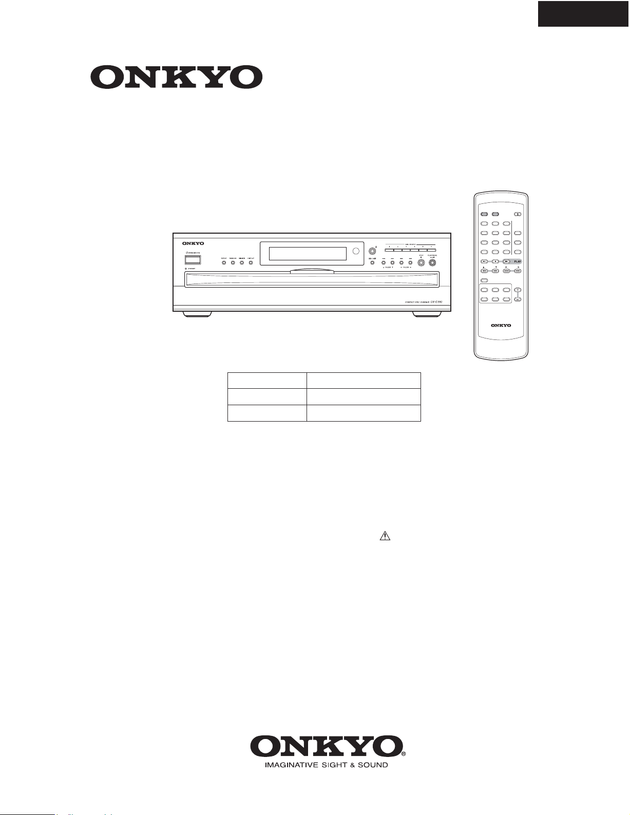
COMPACT DISC CHANGER
MODEL DX-C390
ON STANDBY
123
456
789
SEARCH
>
10/0
10
FOLDER FOLDER
NEXT SELECTION
DISC
1
DISC 2DISC
DISC 4DISC 5DISC
DX-C390
Ref. No. 3782
102003
OPEN / CLOSE
REPEAT
RANDOM
MEMORY
CLEAR
3
DISC
6
Black and Silver models
BMDD
BMPP, SMPP
BMPA
120V AC, 60Hz
230V AC, 50Hz
230-240V AC, 50Hz
SAFETY-RELATED COMPONENT
WARNING!!
COMPONENTS IDENTIFIED BY MARK ON THE
SCHEMATIC DIAGRAM AND IN THE PARTS LIST ARE
CRITICAL FOR RISK OF FIRE AND ELECTRIC SHOCK.
REPLACE THESE COMPONENTS WITH ONKYO
PARTS WHOSE PART NUMBERS APPEAR AS SHOWN
IN THIS MANUAL.
MAKE LEAKAGE-CURRENT OR RESISTANCE
MEASUREMENTS TO DETERMINE THAT EXPOSED
PARTS ARE ACCEPTABLY INSULATED FROM THE
SUPPLY CIRCUIT BEFORE RETURNING THE
APPLIANCE TO THE CUSTOMER.
RC-547C
RC-547C
Page 2

SPECIFICATIONS
2 of 63
DX-C390 (Compact Disc Changer)
Signal readout system Optical non-contact
Frequency response 5 Hz - 20 kHz
SN ratio 98 dB
Audio Dynamic range 96 dB
THD (Total harmonic distortion) 0.005% (at 1 kHz)
Audio output (Digital/Optical) -22.5 dBm
Audio output/Impedance (Digital/Coaxial) 0.5 V (p-p) / 75 ohm
Audio output/Impedance (Analog) 2.0 V (rms) / 470 ohm
Power supply rating AC 120 V 60 Hz (North American model)
AC 230 V 50 Hz (Other than North American models)
Power consumption 10 W (North American model)
8 W (Other than North American models)
Standby power consumption 4 W
Dimensions (W x H x D)
Weight 15.0 lbs. (6.8 kg)
Operating conditions Temperature/Humidity 41-95 F (5-35 C) / 25-80%
Disc compatibility CD, CD-R, CD-RW
17-1/8" x 5-3/16" x 17" (435 x 131 x 432 mm)
DX-C390
RC-547C (Remote Controller)
Transmitter Infrared
Signal range Approx. 16 ft., 5 meters
Power supply Two (AA/R6) batteries (1.5 V x 2)
Specifications and features are subject to change without notice.
Page 3
SERVICE PROCEDURES
3 of 63
PROTECTION OF EYES FROM LASER BEAM DURING SERVICING
DX-C390
This set employs a laser. Therefore, be sure to follow
carefully the instructions below when servicing.
WARNING!!
SERVICE WARNING : DO NOT APPROACH THE
LASER EXIT WITH THE EYE TOO CLOSELY.
IN CASE IT IS NECESSARY TO CONFIRM LASER
BEAM EMISSION, BE SURE TO OBSERVE FROM
A DISTANCE OF MORE THAN 30cm FROM THE
SURFACE OF THE OBJECTIVE LENS ON THE
OPTICAL PICKUP BLOCK.
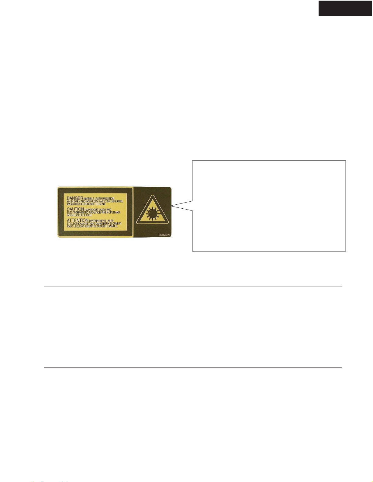
LASER WARNING LABEL
The labels shown below are affixed.
Warning label
Laser Diode Properties
Material: GaAS/GaAlAs
Wavelength: 780nm
Laser output: max. 0.5mW*
Emission Duration: continuous
*This output is the value measured at a distance about 1.8mm
from the objective lens surface on the Optical Pickup Block.
DANGER:
INVISIBLE LASER RADIATION WHEN OPEN AND
INTERLOCK FAILED OR DEFEATED. AVOID DIRECT
EXPOSURE TO BEAM.
CAUTION:
HAZARDOUS LASER AND ELECTROMAGNETIC
RADIATION WHEN OPEN AND INTERLOCK DEFEATED.
ATTENTION:
RAYONNEMENT LASER ET ELECTROMAGNETIQUE
DANGEREUX SI OUVERT AVEC L'ECLENCHEMENT
DE SECURITE ANNULE.
Safety check out
After correcting the original service problem perform
the following safety check before releasing the set
to the customer.
Connect the insulating-resistance tester between the
plug of power supply cord and terminal GND on the
back panel.
Specifications: More than 10 M ohm at 500V.
Initializing the unit
Press "STOP" key and "STANDBY" key at same time.
Displayed "INITIALIZE" on the FL display.
(Only U.S.A. model)
Page 4
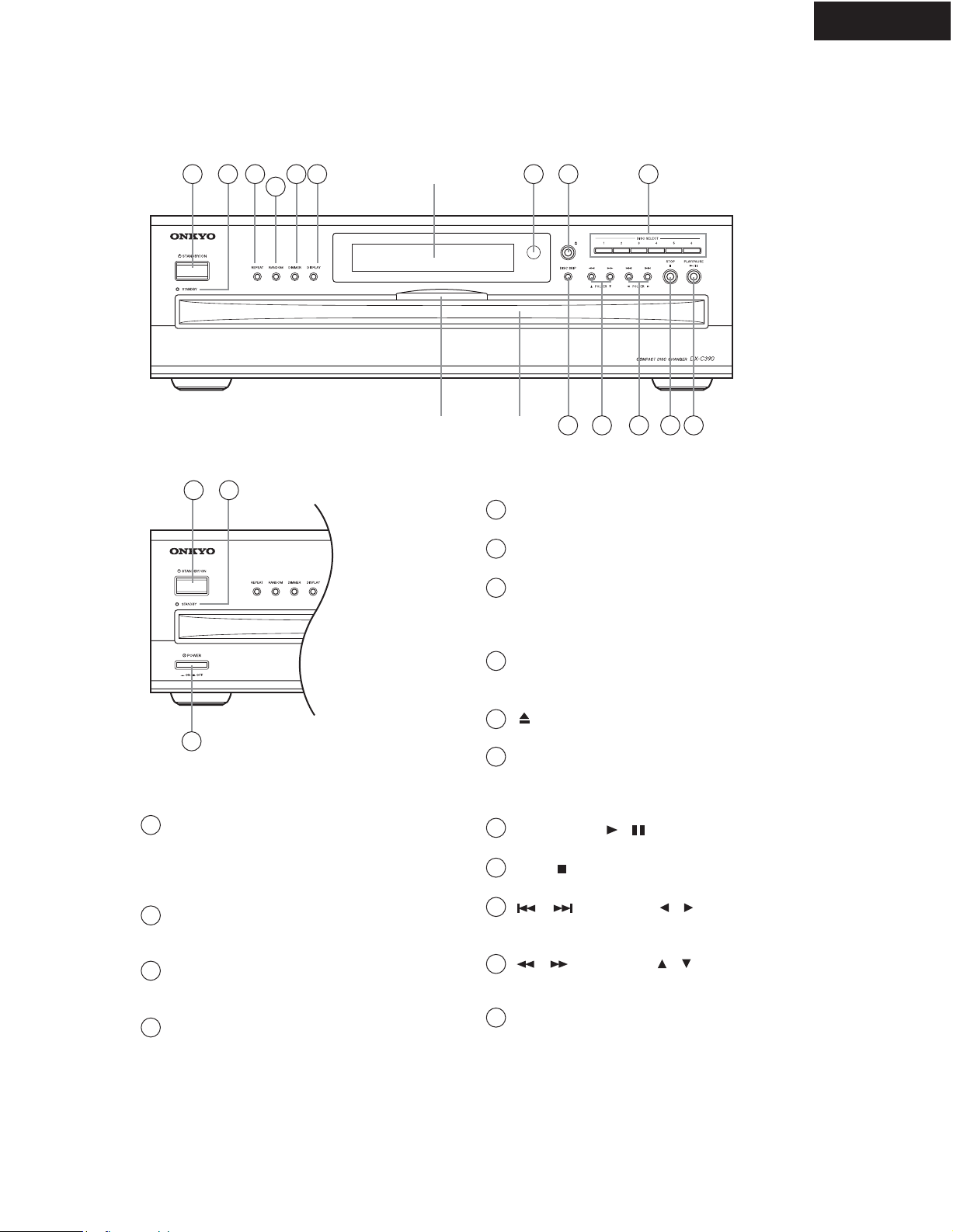
PANEL VIEW-1
4 of 63
FRONT PANEL
North American Model
1
234
DX-C390
7
6
5
Display
9
8
10
Disc tray light Disc tray
Other Models
1
2
For detailed information, refer to the pages in parenthesis.
1
STANDBY/ON button
This button is used to set the DX-C390 to On or
Standby. For models with a POWER switch, this
button has no effect unless that POWER switch is
set to ON.
2
STANDBY indicator
This indicator lights up when the DX-C390 is in
Standby mode.
3
POWER switch (not North American model)
This is the main power switch. When set to OFF, the
DX-C390 is completely shutdown.
4
REPEAT button
This button is used with the Repeat function.
1112131415
RANDOM button
5
This button is used with the Random function.
DIMMER button
6
This button is used to adjust the display brightness.
DISPLAY button
7
This button is used to display elapsed, remaining,
and total time information about the current disc or
track and various information about MP3 tracks.
Remote control sensor
8
This sensor receives control signals from the remote
controller.
[ ] button
9
This button is used to open and close the disc tray.
DISC SELECT buttons
10
These buttons are used to select discs. Playback
starts automatically when a disc is selected with one
of these buttons.
11
PLAY/PAUSE [ ]/[ ] button
This button is used to start and pause playback.
12
STOP [ ] button
This button is used to stop playback.
[ ]/[ ] & FOLDER []/[] buttons
13
These buttons are used to select the previous and
next tracks and to navigate folders on MP3 discs.
[ ]/[ ] & FOLDER
14
These buttons are used for fast reverse and fast forward and to navigate folders on MP3 discs.
15
DISC SKIP button
This button is used to turn the disc tray when loading or removing discs and to select discs for playback.
[]/[] buttons
Page 5
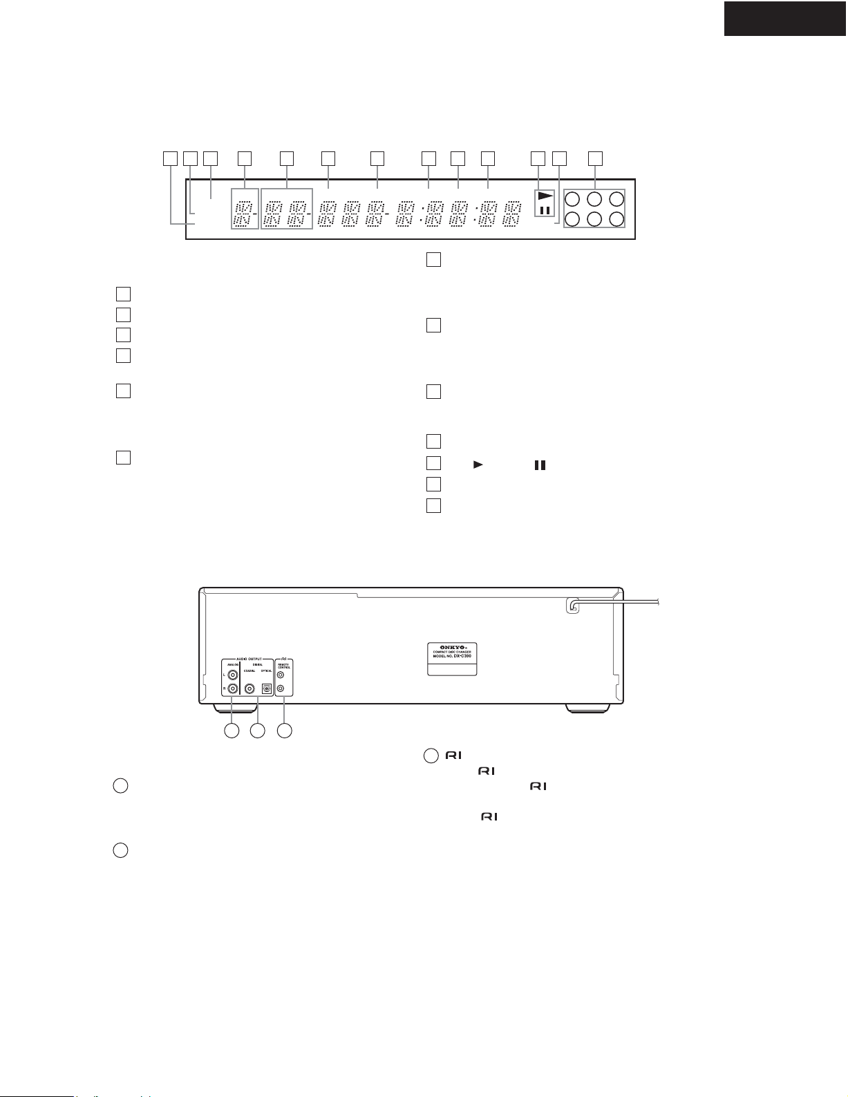
PANEL VIEW-2
5 of 63
DISPLAY
DX-C390
4 5 6
3
FLDR
REPEAT
MEMORY
RANDOM
1
RANDOM indicator
2
MEMORY indicator
3
REPEAT indicator
4
DISC indicator
NEXT TOTALDISC
The number of the current disc appears here.
5
FLDR (FOLDER) indicator
While stopped, the total number of folders on the
current MP3 disc are displayed. During playback,
the number of the current folder is displayed.
6
NEXT indicator
This indicator appears when using the Next Selection function.
7 8 9
TRACK
NAME
7
8
9
10
11
12
13
MP3
12 131 2
3
2
1
6
5
4
10 11
REMAIN
TRACK indicator
While stopped, the total number of tracks on the
current disc are displayed. During playback, the
number of the current track is displayed.
NAME indicator
This indicator appears when the current disc is an
MP3 disc and a name (disc, folder, track) is being
displayed.
TOTAL indicator
This indicator appears when the total remain time is
displayed.
REMAIN indicator
Play / Pause indicator
MP3 indicator
Disc indicators 1 - 6
REAR PANEL
1 2 3
1
ANALOG AUDIO OUTPUT
These RCA/phono connectors can be connected to
the analog audio inputs on a hi-Þ amp or AV
receiver.
2
COAXIAL & OPTICAL DIGITAL AUDIO
OUTPUT
These connectors can be used to connect a CD-R,
MiniDisc, DAT recorder, digital amp, or other
equipment with digital inputs.
3
REMOTE CONTROL
These (Remote Interactive) connectors can be
connected to the connectors on your other
Onkyo AV components for interactive control.
To use you must also make analog audio connections (RCA/phono) between the DX-C390 and
your other Onkyo equipment.
Page 6
PANEL VIEW-3
6 of 63
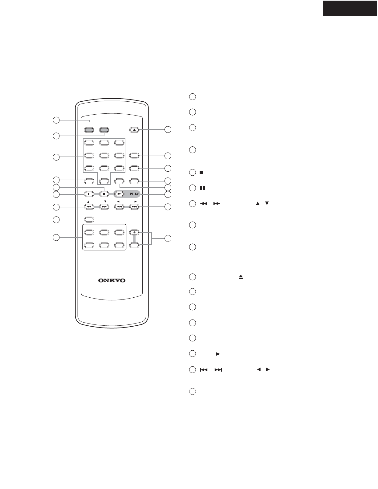
REMOTE CONTROLLER
1
2
3
4
5
6
7
8
9
ON STANDBY
123
456
789
SEARCH
>
10
FOLDER FOLDER
DISC
DISC 4DISC 5DISC
10/0
NEXT SELECTION
1
DISC 2DISC
RC-547C
OPEN / CLOSE
CLEAR
3
6
REPEAT
RANDOM
MEMORY
DISC
10
11
12
13
14
15
16
17
1
ON button
This button is used to turn on the DX-C390.
2
STANDBY button
This button is used to set the DX-C390 to Standby.
3
Number buttons
These buttons are used to enter track and MP3
folder numbers.
4
SEARCH (>10) button
This button is used to enter track numbers above 10
and to select MP3 folders.
[ ] button
5
This button is used to stop playback.
[ ] button
6
This button is used to pause playback.
[ ]/[ ] & FOLDER [ ]/[ ] buttons
7
These buttons are used for fast reverse and fast forward, and to navigate folders on MP3 discs.
8
NEXT SELECTION button
This button is used with the Next Selection function
for cuing up the next track.
9
DISC SELECT buttons
These buttons are used to select discs. Playback
starts automatically when a disc is selected with one
of these buttons.
10
OPEN/CLOSE
[] button
This button is used to open and close the disc tray.
11
REPEAT button
This button is used with the Repeat function.
12
RANDOM button
This button is used with the Random function.
13
MEMORY button
This button is used with the Memory function.
14
CLEAR button
This button is used to cancel various functions.
15
PLAY [ ] button
This button is used to start playback.
[ ]/[ ] & FOLDER [ ]/[ ] buttons
16
These buttons are used to select the previous and
next tracks, and to navigate folders on MP3 discs.
17
DISC [+] & [-] buttons
These buttons are used to select discs.
DX-C390
Page 7
M40
7 of 63
1
DX-C390
A222
A222
A222
2
3
5
M38
4
A222
A221
M38
6
M36
M35
M37
Cloth tape
M34
Cloth tape
(80)
P702
U25
M37
M30
A12
A12
U28
A51
A12
A12
U21
<MPP> <MPA> only
A12
A12
U29
A222
A201
A7
U20-1
A208
A4
A3
A12
A9
A103
A1
A12
A205
A103
A103
0
39
-C
X
D
A103
A301
Page 8
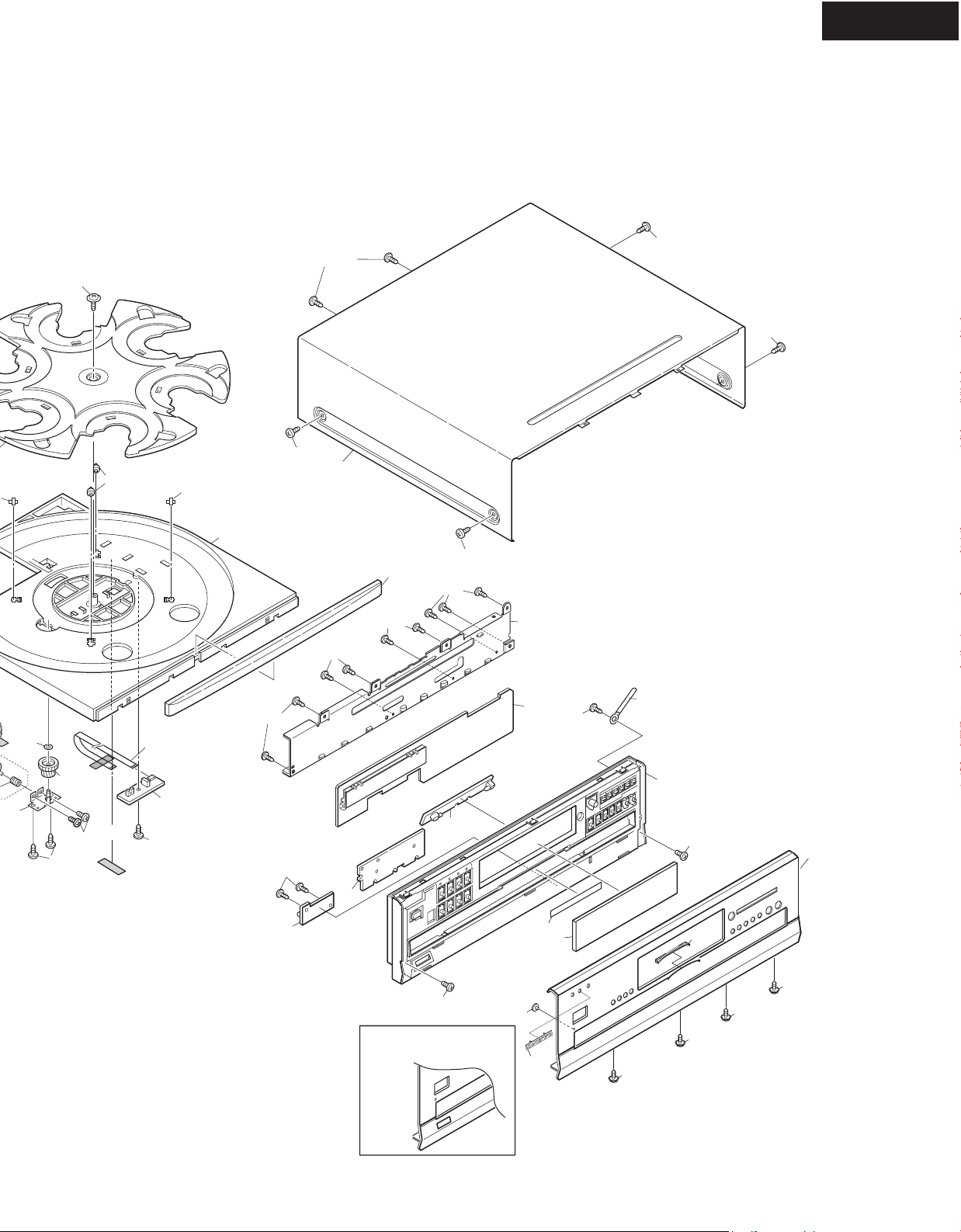
EXPLODED VIEW
8 of 63
P101
P201
A54
M50
A12
A60
A12
M19
M11
M9
M11
M51
M21
U27
M10
M20
M2
M5
M18
M18
M25
A37
C
M3
A37
M8
A12
A12
A12
A12
A37
P701
U23
A12
A103
P901
E101
A24
M14
M17
(BLK)
T901
M18
A103
M14
M17
M12
M13
M14
M41
A103
M24
A103
A29
M18
M16
M14
M16
(WHT)
M23
Cloth tape
A101
M1
U10
M4
M6
C
U22
A12
A19
M7
M11
P701
B
A12
A
D
A12
A37
D
P904
B
A
P102
P102
A37
M52
A20
A55
U26
M53
M32
M30
M39
M54
Cloth tape
M33
M38
M31
(Bracket + Shaft)
M36
U24
A18
A122
U30
A121
A313
<MPP> <MPA> only
A311
A42
A37
A41
A42
A42
A37
A16
A41
A42
Page 9
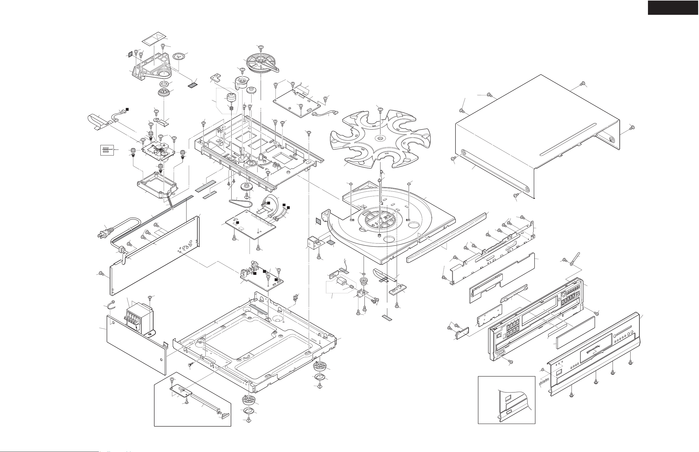
EXPLODED VIEW
9 of 63
A103
E101
U24
P101
P901
P201
A24
A54
M50
M14
M17
(BLK)
T901
C
M18
A103
M18
M14
M17
M12
M13
A12
M18
M41
A103
M14
M24
A103
A29
A60
M18
M16
A12
M21
M20
M25
M19
M14
M16
(WHT)
M23
M51
U27
M5
A37
Cloth tape
A101
M1
U10
M2
M10
M3
M4
M11
M6
C
U22
M9
A12
A37
A19
M11
M8
M11
P701
A12
M7
B
A12
A12
A
D
A12
A37
D
A12
P904
B
A12
A37
A
P102
P102
A37
M52
A20
P701
U23
A55
U26
M53
M32
M30
A12
M54
Cloth tape
M33
M39
M38
(Bracket + Shaft)
A16
M31
M36
M40
1
M35
M37
6
Cloth tape
2
M34
5
M38
Cloth tape
(80)
DX-C390
A222
A222
A222
3
4
A222
A221
M38
M30
A222
A51
A12
A12
A12
A12
P702
U25
U29
M37
A12
U21
U28
A7
U20-1
A4
A3
A12
A9
A1
A12
A205
A301
0
39
-C
X
D
A18
A122
U30
A121
A313
<MPP> <MPA> only
A311
A42
A37
A41
A42
A42
A37
A41
A42
A12
<MPP> <MPA> only
A201
A208
A103
A103
A103
A103
Page 10
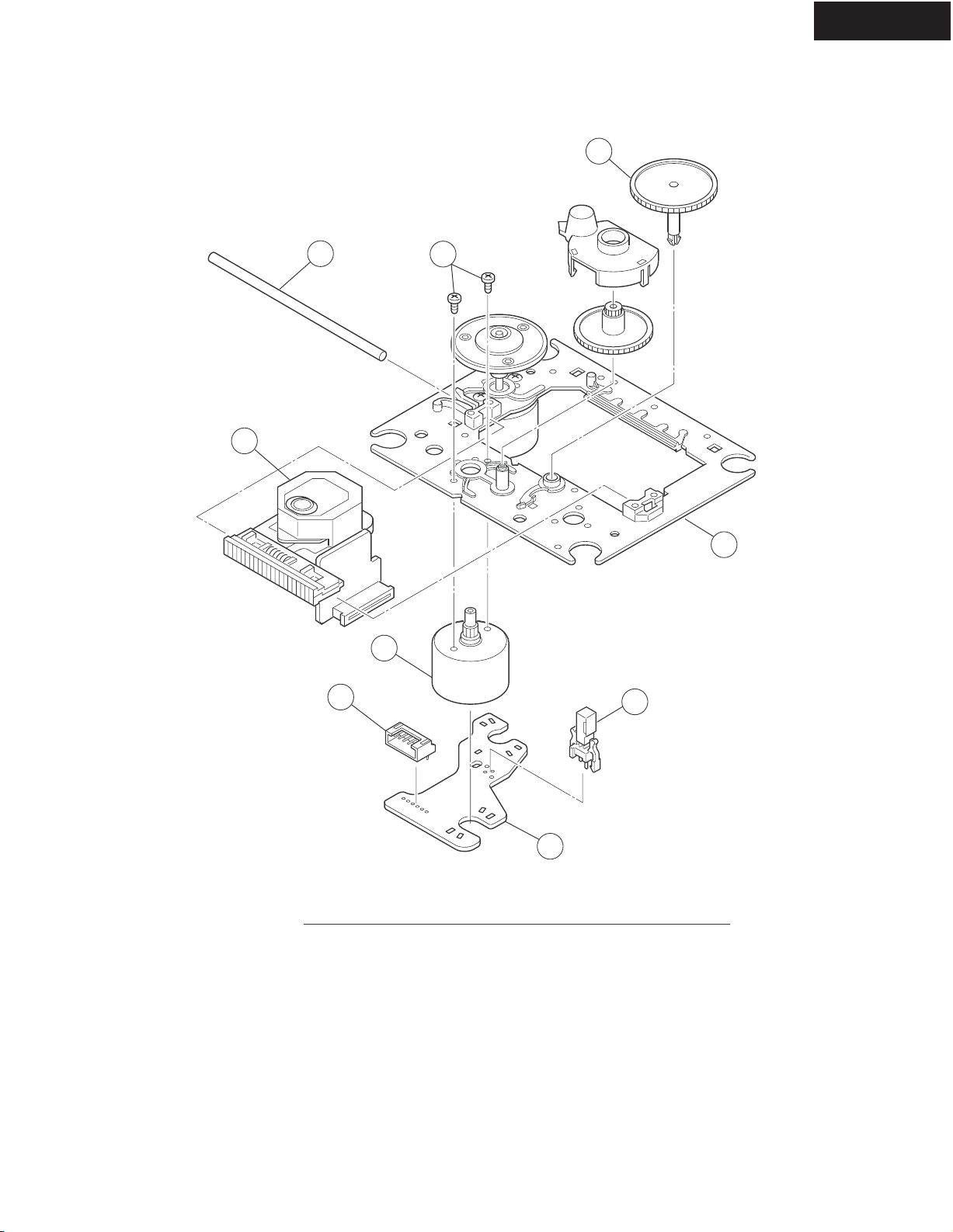
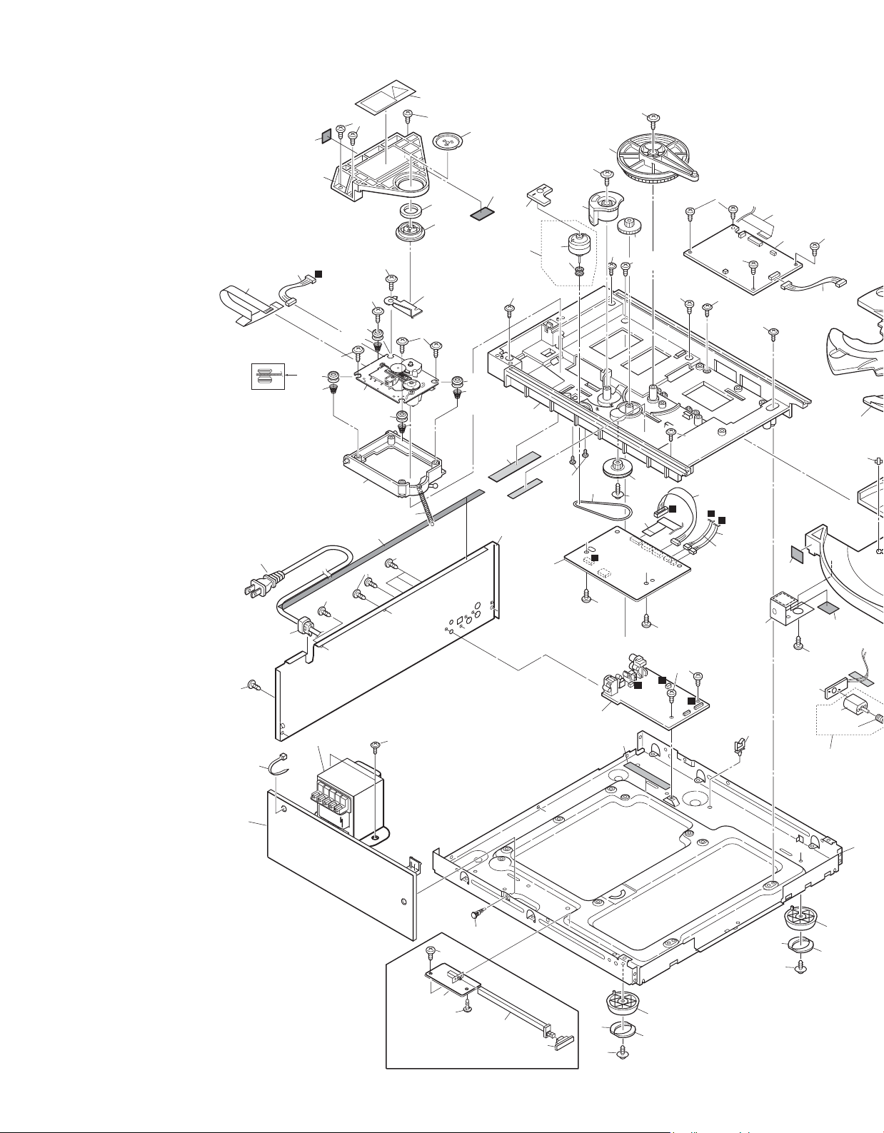
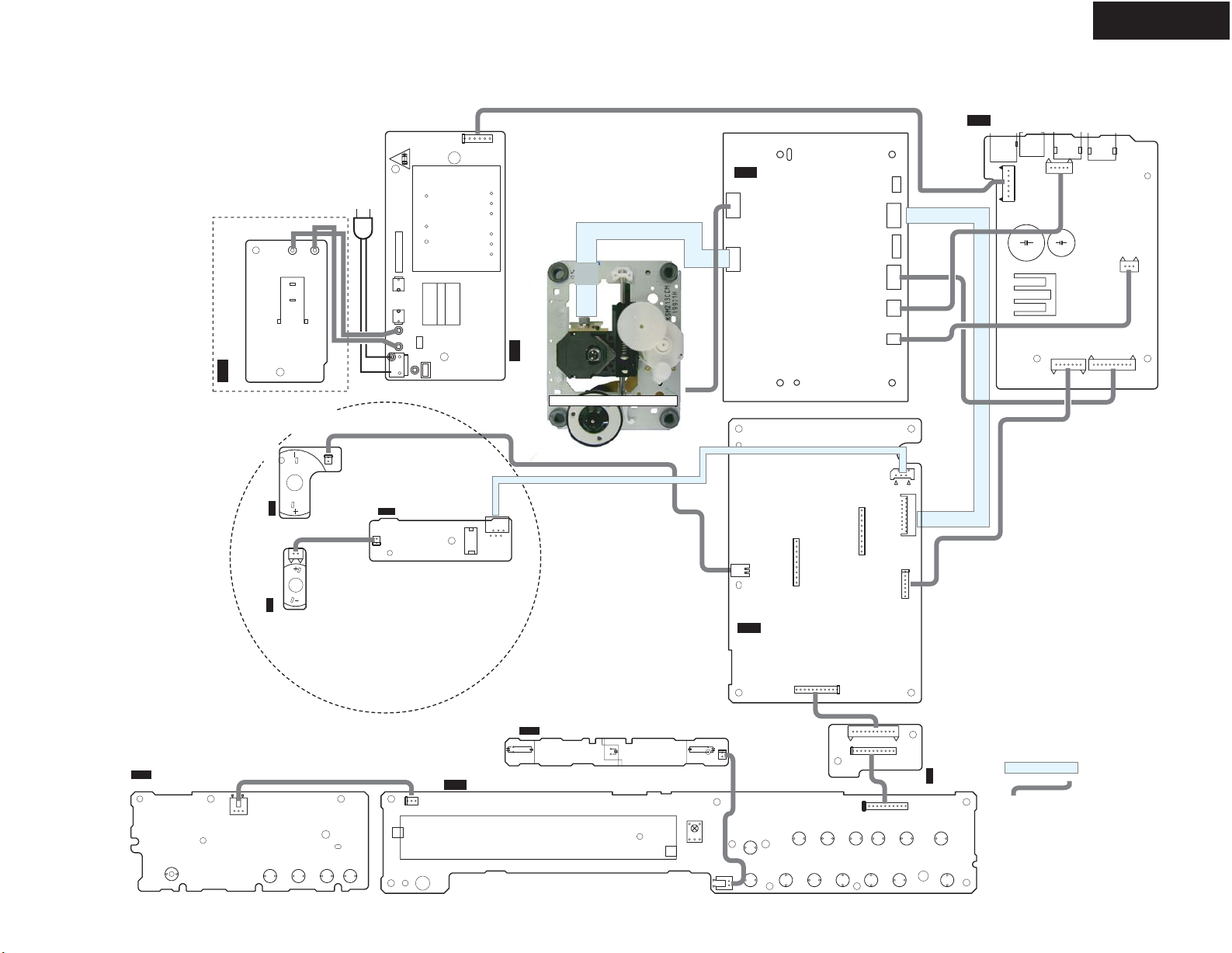
EXPLODED VIEW OF MECHANISM
10 of 63
CD DRIVE UNIT : KSM-213CCM
DX-C390
54
61
53
58
55
51
52
56
PARTS LIST
REF. NO. PART NO. DESCRIPTION
51
52
53
54
55
56
57
58
61
X-2625-877-1
X2625-769-1
2626-908-01
24810023
7621-255-15
24840008
1639-678-12
1-564-722-11
8848-483-05
57
Motor chassis ass'y
Motor gear ass'y
Sled shaft
Gear (A) (S)
P2 x 3, Screw
Leaf switch
Motor PC board
Connector 6pin
KSS-213C, Pickup
Page 11
A
11 of 63
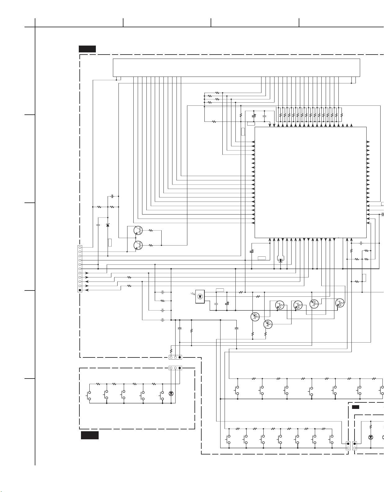
SCHEMATIC DIAGRAM-2
U20 : DISPLAY CIRCUIT PC BOARD NADIS-8054
BCDEFGH
F111
F122
G15
G26
G37
G48
1
G59
G1014
G610
G1115
G711
G812
G913
2
C809
104
R829
R830
470
470
223
D804
C810
F1 ROT-R
3
F1
F2
F2
FL-B
VDISP
5V
GND
GND
SUBRST
SUBCL
SUBREQ
SUBSI
SUBSO
P752A
To CONNECTION PC BOARD NAETC-8062
SUBREQ
SUBSI
UDZS11B
-30
SUBRST
GND
SUBCL
SUBSO
R803
330
R802
330
Q803
2SC2859
Q804
2SC2859
R831
22K
R832
22K
C811
223
R801
10K
C812
330
C813
330
4
G1216
C816 101
R880 NC
R881 NC
R882 NC
R883 NC
SPS-440-1-VP
NC
R833
Q802 HNV-12SM57
R899
0
4.9
104
C802
Q810
C801
100/6.3
R836
R834
100
100K
5.0
Q807
RN2402
101
C814
-30
C804
C808
R806
61
62
63
64
65
66
67
68
69
70
71
72
73
74
75
76
77
78
79
80
10/16
R835
100
56
2.2/50
12G
11G
10G
9G
8G
7G
6G
5G
4G
3G
2G
1G
5.0
P140
C807
P4
P3
P2
P1
FIP15
FIP14
FIP13
FIP12
P241
R805
P342
P443
223
59
60
VDD2
VDISP
VDD1
VSS12X13X2
1
DTC114YKA
Q806
RN2402
680
P544
P645
P746
R884 NC
R885 NC
R886 NC
P558P657P756P855P9
IC
5
4
X801
5MHZ
Q809
DX-C390
CDC-3.4
P1049
P1150
P1251
P1352
P1453
P1554
R891 100K
R892 100K
R893 100K
P1655
R894 100K
P847
P948
R887 NC
R888 100K
R889 100K
R890 100K
54
P1053P1152P1251P1350P1449P1548P1647P1746P1845P19
Q801
MPD780232GC
GEND2
RESET
6
DTC114YKA
GND1
SUBCL7SUBREQ
SUBSI8SUBSO9TRAYLED114TRAYLED2
Q808
R805
680
330
STBYLED
12
11
13
10
Q805
RN2402
R895 100K
P1756
IRIN
15
R896 100K
P1857
R897 100K
16
P1958
44
FIP3543FIP3642FIP37
AVSS
18
Q811
F2161
R898
100K
41
KEY220KEY3
19NC17
R837
DTC114YKA
F2262
FIP38
FIP39
FIP40
FIP41
FIP42
FIP43
FIP44
FIP45
FIP46
FIP47
FIP48
FIP49
FIP50
FIP51
FLON 26
VDD0 25
AVDD 24
VSS0 23
KEY0 22
KEY1 21
C815
101
0
R807
2.7K
R826
2.7K
40
39
38
37
36
35
34
33
32
31
30
29
28
27
R827
2.7K
R828
2.7K
5.0
5.0
C806
104
470
R804
STANDBY/ON
D801
SLR-342VR
P801A
P801B
GND
S813
S806
DISC SKIP
R813
390
S814
OPEN/CLOSE
R808
390
R814
DISC1
S811
P802A
STOP
R820
D802
R819
3.9K
56
S812
R821
D803
SELU2L10C
S819
S810
R812
1.8K
UP
U29 : ILLUMINATION PC BOARD
NADIS-8066
P802B
DISC6
S808
R816
1K
DISC3
R810
820
FF
R817
1.8K
S817
DISC4
R809
470
FR
S807
R815
820
470
S815
S816
DISC2
S809
S818
DOWN
R818
3.9K
DISC5
R811
1K
NADIS-8054
NASW-8055
S801
R8251KR824
S802
DISPLAY
820
DIMER
S803
R823
470
RANDOM
S804
R822
390
REPEAT
S805
5
U21 : STANDBY LED PC BOARD
NASW-8055
Page 12
DX-C390
12 of 63
A
SCHEMATIC DIAGRAM-2
U20 : DISPLAY CIRCUIT PC BOARD NADIS-8054
1
2
C809
104
R829
R830
470
470
223
D804
C810
F1 ROT-R
3
F1
F2
F2
FL-B
VDISP
5V
GND
GND
SUBRST
SUBCL
SUBREQ
SUBSI
SUBSO
P752A
To CONNECTION PC BOARD NAETC-8062
4
NADIS-8054
NASW-8055
R8251KR824
S801
DISPLAY
5
U21 : STANDBY LED PC BOARD
NASW-8055
SUBREQ
SUBSI
S802
UDZS11B
-30
SUBRST
GND
SUBCL
SUBSO
820
DIMER
BCDEFGH
F111
F122
S803
R803
330
R802
330
R823
470
RANDOM
G15
G26
G37
Q803
2SC2859
Q804
2SC2859
S804
G48
G59
R831
22K
R832
22K
R822
390
REPEAT
G610
S805
G711
C811
223
R801
10K
C812
330
C813
330
G812
G1014
G1115
G913
470
R804
STANDBY/ON
D801
SLR-342VR
G1216
C816 101
P801A
P801B
R880 NC
R881 NC
R882 NC
R883 NC
SPS-440-1-VP
NC
R833
Q802 HNV-12SM57
R899
0
4.9
104
C802
Q810
C801
GND
S813
R836
R834
100
100/6.3
RN2402
C814
S806
DISC SKIP
R813
390
S814
OPEN/CLOSE
5.0
Q807
101
100K
-30
C804
C808
R806
R808
390
R814
DISC1
F2161
P140
P241
P342
P443
P544
R884 NC
223
C807
2.2/50
59
60
P558P657P756P855P9
VDD2
VDISP
P4
61
P3
62
P2
63
P1
64
FIP15
65
FIP14
66
FIP13
67
FIP12
68
12G
69
11G
70
10G
71
9G
72
8G
73
7G
74
6G
75
5G
76
4G
77
3G
78
2G
79
1G
80
VDD1
VSS12X13X2
1
10/16
5.0
X801
5MHZ
R835
100
Q809
DTC114YKA
Q806
RN2402
56
680
R805
R809
470
FR
S807
R815
820
470
S815
S816
DISC2
P1049
P645
R885 NC
P1150
P746
P847
P948
R886 NC
R887 NC
R888 100K
R889 100K
54
P1053P1152P1251P1350P1449P1548P1647P1746P1845P19
Q801
MPD780232GC
IC
RESET
SUBCL7SUBREQ
SUBSI8SUBSO9TRAYLED114TRAYLED2
5
4
6
Q808
DTC114YKA
R805
680
DX-C390
330
CDC-3.4
R810
820
FF
S808
R816
R817
1K
1.8K
S817
DISC3
DISC4
R890 100K
S809
P1251
10
S818
R891 100K
P1352
R892 100K
GND1
11
Q805
RN2402
DOWN
P1453
R893 100K
GEND2
12
R818
3.9K
DISC5
P1554
P1655
R894 100K
R895 100K
STBYLED
13
R811
1K
S819
P1756
IRIN
15
S810
R896 100K
P1857
R897 100K
16
DISC6
F2262
P1958
R898
100K
44
41
FIP3543FIP3642FIP37
FIP38
40
FIP39
39
FIP40
38
FIP41
37
FIP42
36
FIP43
35
FIP44
34
FIP45
33
FIP46
32
FIP47
31
FIP48
30
FIP49
29
FIP50
28
FIP51
27
FLON 26
VDD0 25
AVDD 24
VSS0 23
KEY0 22
KEY1 21
AVSS
KEY220KEY3
18
19NC17
C815
101
R827
0
R837
2.7K
R807
R828
2.7K
2.7K
5.0
R826
2.7K
DTC114YKA
Q811
S811
P802A
STOP
R820
D802
R819
3.9K
56
S812
SELU2L10C
R812
1.8K
UP
U29 : ILLUMINATION PC BOARD
NADIS-8066
P802B
U25 : DISC SENSOR
5.0
PC BOARD NAETC-8059
NAETC-8059
C806
104
5.0
180
R651
R652
5.0
330
R653
R654
STOP POS SENSOR
U26 :ROULETTE MOTOR
PCB NAETC-8060
NAETC-8060
LOADING MOTER
Z702
NAETC-8061
PLAY/PAUSE
56
R821
D803
U27 :LOADING MOTOR
PCB NAETC-8061
NC
R838
NC
D805
SELU2L10C
NADIS-8066
DISC SENSOR
R6560R655
0
Q651
GP2S28
223
150K
C653
Q652
RPI-576
223
470K
C654
P703A
Z701
ROULETTE MOTER
104
C655
104
C656
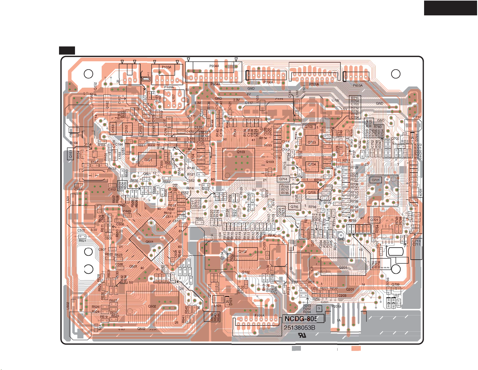
U23 : MECHANISM CONTROL PC BOARD NADG-8057
5.0
5.6K
DTC114YKA
R607 0
D604
R627
2.2K
Q608
2SA1162
R617
Q603
Q605
NC
R608
UDZS4.7B
R606
R610
10K
R622
100K
22K
10K
R628
R605
IN19
D601
UDZ2.2B
UDZ2.7B
10K
R616
DISC-SENS
R602
Q607
DTC114YKA
B+5V
223
C609
C610
100K
223
C611
NAETC-8062
R601
100K
MGND
MECHA-POWER
223
SOSICL
SUBSO
SUBSI
Q601
TA7291S
GND5
IN21
NC4
OUT17
OUT23
VCC2
223
C602
C601
0
100K
R614
S601
SPVF1
8.7
10K
VREF8
VS6
R603
2.2K
R604
R615
S602
SPVF1
D602
4.7
1/2W
5.0
10K
S603
SPVF1
100/16
U28 : CONNECTION PCB
NAETC-8062
R618
3.3K
Q604
DTC114YKA
R621
8.2K
R619
270K
NC
C603
C652 104
P702B
C604
P702A
Q602 TA7291S
IN21
VCC2
P703B
223
C607
LOADING+
LOADING-
8.7
P704A
P704B
C605
NC
OUT23
C606
R613
8.2K
R624
NC4
104
GND5
100/16
4.7 1/2W
R620
1M
5.0
Q606
DTC114YKA
R626
OUT17
VS6
R609
220
D603
10K
R612
R611
5.6K
DTC114YKA
R623
4.7K
R625
1M
RULETTE+
RULETTE-
IN19
VREF8
UDZS4.3B
NC
C608
STOPSENS
ROT-L
ROTH
LOD-R
LOD-L
CURRENT
LOAD-SW1
LOAD-SW2
LOAD-SW3
8.7
REQ
RST
SUBCL
SUBEQ
NADG-8057
ROT-R
ROTH
LOAD-SW3
ROT-L
LOAD-SW1
CURRENT
LOAD-SW2
LOD-R
STOPSENS
LOD-L
DISC-SENS
5V
GND
GND
SUBRST
REQ
RST
SO
CL
SI
5.0
VDISP
ROT-R
ROTH
LOAD-SW3
ROT-L
LOAD-SW1
CURRENT
LOAD-SW2
LOD-R
STOP-SENS
LOD-L
DISC-SENS
SUBREQ
SUBRST
SUBSO
SUBCL
SUBSI
P701B
B5V
GND
F2
F1
VDISP
MGND
BMECHA
P705A
P751A
F2
F1
P751B
P752B
To Main circuit PC board NADG-8053
To OUTPUT TERMINAL
PC BOARD NAAR-8056
Page 13
DX-C390
13 of 63
SQSO
SQCK
CDXLT
MSO
CLOK
SENS
SCLK
SCOR
R124
R128
470
330
R130
R129
1.5K
8
7
18
17
16
C4M
WDVK
DVSS0
ADIO
RFDC
AVSS045AVSS1
44
43
R137
C118
103
C117
0.47/50V
1
2
3
C703 104
4
5
6
470
78
MSCK
R751
47K
R710
R729 470
680
23
22
21
CDCOM
SENSI
MP3CE
CDSUBQ
SUBCL
SUBSI
MP3COM
SUBSO
SUBRST
DOUT
MSCK
MSO
MSI
GND1
TXD
RXD
AVREF
ANO1
ANO0
AVSS
AN17
AN16
AN15
ANI278ANI379ANI4
80
104
10K
9
15
13
12
11
10
14
GFS
SCLK
ATSK
SENS
XPCK
C2PO
XUGF
SCOR
WFCK
Q103
CXD3068Q
IGEN
ASYI49ASYO
FILI54FILO
RFAC
AVDD0
CLTV
46
48
53
50
47
51
52
33K
10K
R138
R141
100K
R139
152
C120
3.3
B+3.3V
MP3CL MP3CL DITPD
Q703
14
13
12
11
10
9
TC74VHCT08AFT
R715 470
R753
47K
47K
R750
R749
1.2K
XRST
LDON
SCLK
CDXLT A0
470
R727
R746
R752 2.2K
R728 470
20
19
18
17
16
15
14
13
12
11
10
9
8
7
6
5
4
3
2
1
MP3INTB
IR.IN
C702
10K
R726
470
MSI OE
C701
330
R748
104
R702
C712
NC
330
R701
5.0
10/16
R122
R126
2.2K
R125
2.2K
R127
2.2K
2.2K
C110
473
330
104
C111
4
1
3
2
5
6
DVDD0
XLAT
DATA
XRST
CLOK
MUTE
EKCK
80
SBSO
79
SCSY
78
SQCK
77
SQSO
76
XOLT
75
SOCK
74
SOUT
73
XTAO
72
XTAI
71
DVSS2
70
XTSL
69
EMPH
68
BCK
67
PCMD
66
LRCK
65
DOUT
64
MD2
63
ASYE
62
61
DVDD2
BIAS
PCO
V16M59VCTL58VPCO
AVDD1
57
55
60
56
104
C124
3.3
3.3K
R143
470K
R144
1M
R142
3.3K
104
R136
C122
473
C121
10K
R140
1M
C119 221
MSO
XRST
SCLK
CDXLT
XRST
1K
R712
470
R711
470
R731
MP3INTB
R706
1K
0
R755
MSO
R747
1K
R703
1K
330
R705
100K
R725
C151
150
C152
180
330
R121
C126
104
C2PO
R145
1M
R146
330
C125
104
C123 330/6.3
R165 1
470
R516
470
470
R517
R515
R166 NC
R562 NC
R565 NC
R564 NC
CDLRCK
CDPCM
CDBCK
CDLRCK
MP3CE
C2PO
5.0
47K
R704
R760
RXD
0
TXD
0
IR.IN
P853A
DOUT-SEL
5V
GND
RXD
TXD
IR.IN
NC
X151
16.9344MHZ
R152 1M
R151 220
L158
BLM21B222SPT
3.3
R510
2K
4
3.3
L104
BLM21B222SPT
MCLK
R505
C504
330
R509
3.3K
R511
150
Q151
TC7WU04FU
758
R153
2.2K
1K
R156
470
R503
470
470
R501
C503
104
1236
R154
R563
NC
L501
BLM21B222SPT
C501
104
C502
220/6.3
3.3
C505
105
C506
104
NAAR-8056
2.2K
1K
R155
P102B
P102A
3.0
R768 47K
R767 47K
DOUT-SEL
470
R507
DEEMPH
MUTE
MSO
INTB
CDPCM
CDBCK
R552
0
473
C512
80
79
LRSY
1
DATAIN
DATACK
ADDATA
2
ADBCK
3
ADLRCK
4
C2FIN
5
TEST1
6
CKIN
7
VSS
8
CKOUT
9
TEST2
10
DVDD1
11
PW
12
SBSY
13
SFSY
14
SBCK
15
AVDD
16
VPRFR
17
VCOC
18
VPDO
19
AVSS
20
VSS1
DVDD2
21
22
104
C507
C301
R301
1.5K
22/35
C303
C304
C302
R302
1.5K
22/35
ADLRCK
ADBCK
ADDATA
12345678
GND
REFNCBCK
DATA
LRCK
AOUTR
WM8726
MCL
FORMAT
EMPHNCMUTE
AOUTL
VDD
9
10
111213
14
C159
1
2
3
4
Q153
5
6
TC74VHCT00AFT
78
470
R561
470
R518
R514
2.2K
R513
2.2K
R512
1K
77
71
76
75
74
73
72
78
CL
CE
OVF
INTB
RESB
CMDIN
CNTOK
CMDOUT
Q501
LC78683E
MDATA023MDATA1
MDATA225MDATA326MDATA427MDATA528MDATA629MDATA730MDATA833MDATA9
24
0
R5260R5250R5240R5230R5220R5210R5200R519
DATA0
DATA1
DATA2
DATA3
DATA4
DATA5
DATA6
DATA7
102
102
Q152
BLM21B222SPT
WOK
DVDD3
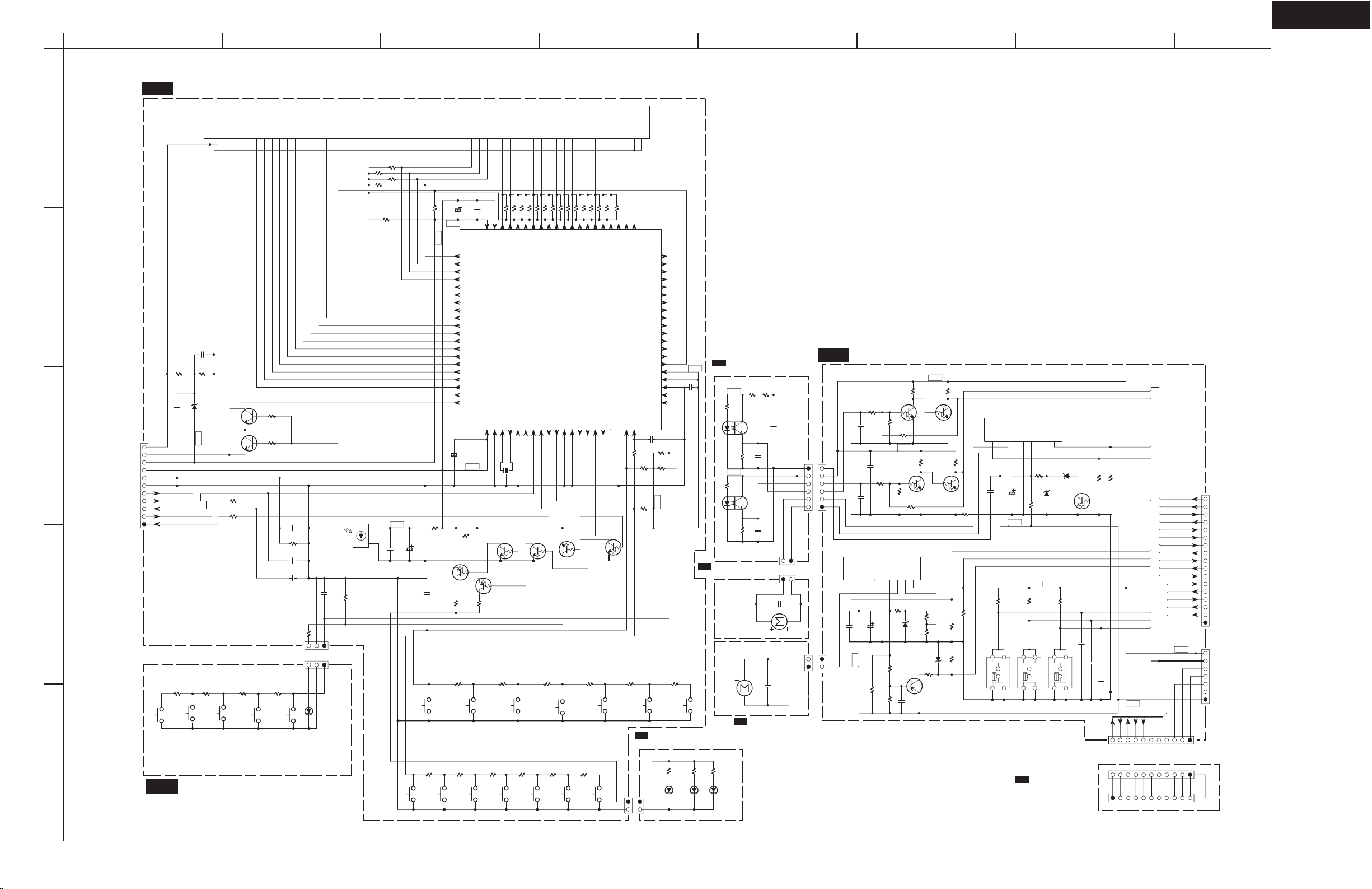
U22 : OUTPUT TERMINAL PC BOARD NAAR-8056
R303
R341
470K
C305
C306
R342
470K
R304
L154
R164
220/6.3
BLM21B222SPT
14
13
12
11
10
9
R502
470
R506
470
DITDO
DITCL
DITDI
C511 104
69
68
70
VSS5
DVDD6A
VSS2
31
32
0
DATA8
DATA9
R305
10K
5
7
Q301
6
NJM4580M-D
10K
272
272
NJM4580M-D
10K
2
Q302
1
3
R306
10K
C157
47/6.3
Q154
MPC29L05T
IO
G
18
L151
5.0
R158
104
C164
R163
NC
R508
470
R504
470
DITCE
R555
470
473
10K
R556
C551
C510
R560 470
62
66
65
64
63
67
VSS4
STCK
CRCF
MADRS0
FSYNC
STREQ
STDATA
MADRS1
MADRS2
MADRS3
MADRS4
MADRS5
MADRS6
MADRS7
MADRS8
MADRS9
MADRS10
MADRS11
MADRS12
MDATA1035MDATA1136MDATA1237MDATA1338MDATA1439MDATA15
34
DATA10
DATA11
DATA12
DATA13
DATA14
8.7
470
DVDD4
CASUB
CASLB
R5340R5330R5320R5310R5300R5290R5280R527
R307
1.5K
R308
1.5K
1
2
3
4
5
6
7
8
9
10
11
12
104
61
VSS3
OEB
WEB
40
DATA15
V1
TRANS
PDN
MCLK
SDTI
BICK
LRCK
CSN
CDTI
CCLK
CDTO
C1
DVDD6
RASB
3.3
C307
C308
NC
C177
1
2
3
4
5
6
GND7
Q551
AK4103VF
60
59
58
57
56
55
54
53
52
51
50
49
48
47
46
45
44
43
42
41
C508
R309
22K
182
182
R310
22K
R332
1K
R333
1K
D301
CKSO
R559
R550
R549
R548
R547
R546
R545
R544
R543
R542
R541
R540
UCAS
LCAS
104
22K
R311
22K
R312
4.7
UDZ4.7B
BLM21B222SPT
VCC 14
13
12
11
10
9
8
Q155 TC74VHCU04FT
U1
24
DIF2
23
DIF1
22
DIF0
21
TXP
20
TXN
19
VSS
18
VDD
17
CKSI
16
15
BLS
14
ANS
13
A1
A2
A3
A4
A5
A6
A7
WE
L155
R319
22K
2
3
5
6
R320
22K
C315 104
R557
0
0
0
0
0
0
0
0
C509
104
0
0
0
0
Q301
R336
Q302
DTA124EKA
10K
4
8
0
8
4
Q307
R334
C176
R317
1.5K
NJM4580M-D
NJM4580M-D
R318
1.5K
10K
NSRF-2046
NC
C171
5.0
104
C170
470
C552
104
R558
2.2K
R536 0
1
R313
22K
R314
22K
7
R161
NC
R159
L156
R551
R535 0
R335
0
R315
1.5K
R316
1.5K
75
L157
C172
0
BLM21B221SB
L503
BLM21B222SPT
5.0
L502
BLM21B222SPT
3.3
6
Q303
7
22/35
5
NJM4580M-D
C311
220/16
C312
220/16
7.0
NJM4580M-V
8
3
1
Q303
2
22/35
4
R330
120 (1/2)
-8.0
R329
1K
NC
R162
P103B
P103A
1
224
C173
NC
R160
100K
VS3
VC
50
1
DQ16
DQ1
49
2
DQ2
DQ15
3
C513
DQ3
4
DQ4
5
VC2
6
DQ5
7
DQ6
8
DQ7
9
DQ810DQ9
NC1
11
NC2
15
NC3
16
WE
17
18
A11R
19
A10R
20
A0
21
A1
22
A2
23
A324A4
VC325VS
C514
48
DQ14
47
DQ13
46
VS2
45
DQ12
44
DQ11
43
DQ10
42
41
NC5
40
IC41LV16100-50T
NC4
36
LCAS
35
UCAS
34
OE33RAS
A9R
32
A8R
31
A7
30
A6
29
A5
28
Q502
27
26
R538
0
104
DATA2 DATA13
DATA3 DATA12
DATA6 DATA9
A10 A8
A0 A7
A1 A6
A2 A5
A3 A4
R539 0
R537 0
220/6.3
C309
C310
R331
R321
470K
R322
470K
120 (1/2)
C174 102
L152
BLM21B222SPT
R323
470
R328
470K
R325
1K
2SD655
R327
470K
2SD655
R326
1K
R324
470
L159
BLM21B222SPT
C167 104
L153
BLM21B222SPT
R148
470
Q305
Q306
C168
10/16
P151
C175
NC
P152
5
Q156
TOTX179
C165
P153
104
1
2
C166
3
104
4
Page 14
A
14 of 63
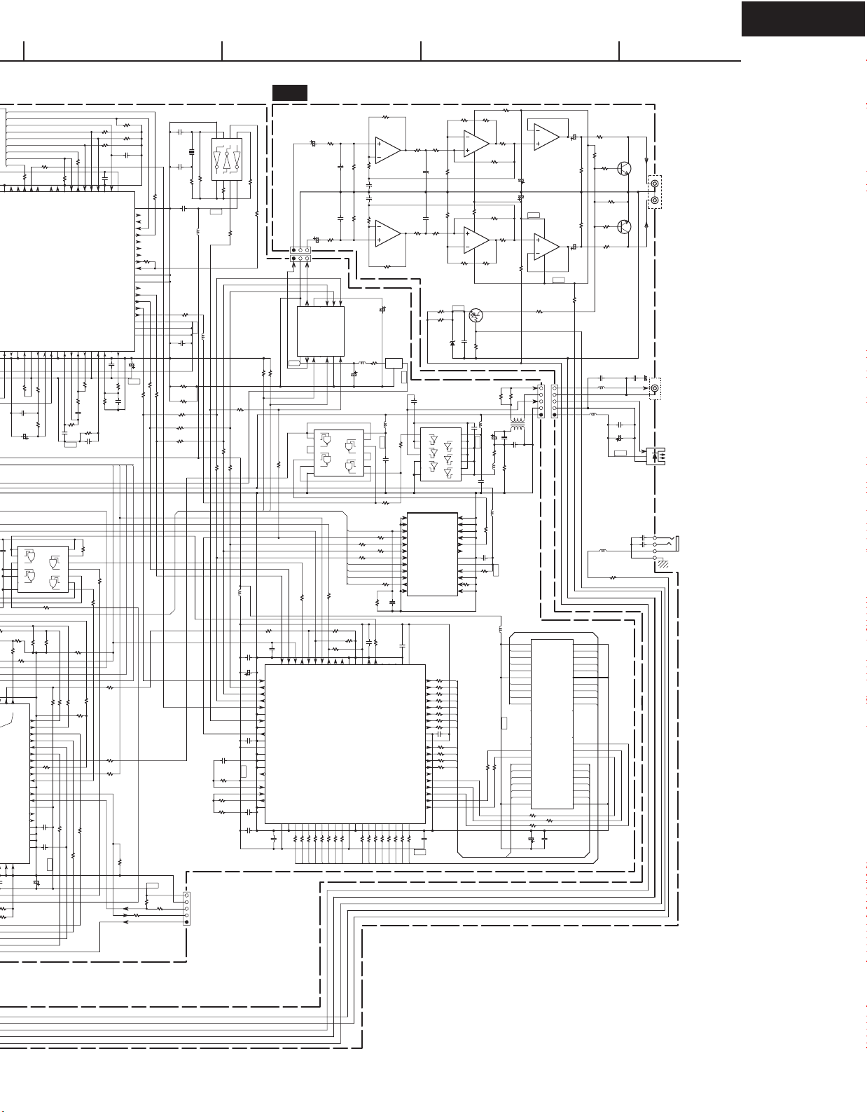
SCHEMATIC DIAGRAM-1
KSM-213CCM
FC-
TR-
TR+
FOCUSING
TRACKING
1
+5V
Vref
SPINDLE MOTOR
2
THREAD MOTOR
FC+
PD
VR
LD
LD-G
F
C
B
A
D
E
VCC
VC
LS
M5
BCDEFGH
U10 : MAIN CIRCUIT PC BOARD NADG-8053
R123
3.3
C103
C106
C108
100/6.3
1.6
R206 47K
7
OPOUT2
OPOUT322OPOUT4
18K
R210
0
10/16
LDON
EE
C102
104
R201 10K
C201 333
1
6
4
FWD
OPIN1+2OPIN1-3OPIN2+5OPIN2-
OPOUT1
REV
OPIN4+
OPIN3+24OPIN3-
OPIN4-
28
25
23
27
26
332
RFAC
15
FE1
DVC
14
DVCC
13
TE BAL
SW
12
F
11
E
CE1
10
D
VCC
9
C
RFG
8
B
BST
724
Q102 CXA2581N
A
VFC
6
VEE
5
RFC
AC SUM
4
EQ IN
RFDCO
3
PD
2
RF DC
LD
1
DC OFSET
2.5
DVC
R205
R213
R214
8.2K
C207 681
P101A
FC-
TR+
TR-
FC+
PD TE
GND
LD FF
F D
C C
B B
A A
D
E
VC
R10547R104
D101
1SS355
TR+
TR-
L101
100K
V01+14V01-13V02+12V02-
FC-
FC+
V04+15V04-
16
L202
C210
BLM21B222SPT
330/6.3
B+5V
P201A
SP+
SP-
SL+
SL-
SSTOP
R102 10K
R101 10K
47
Q101
2SA1162
V03+17V03-
PD
5.0
11
V0L+10V0L-
GND
18
19
104
C107
1.6
C109
C101
100/6.3
9
8
VCC
Q201 BA5984FP
BIAS
MUTE
20
21
1.6
CDPOWER
104
103
C203
C205 122
B+3.3V XRST
FE
16
R107
17
100K
TE
18
19
CE
20
21
22
23
25
26
VC
27
28
29
30
R204
100K
10K
C202
8.2K
C206
333
681
R202
47K
R110
150K
R117
39K
R209
R208 47K
R207 47K
R108
R109
10K
10K
5
R111
R112
6.8K
15K
R113
R114
10K
10K
R115
R116
18K
5.6K
RFDC
R119
R118
5.1K
330/6.3
18K
R120
8.2K
3.3K
C131330/6.3
C104
C105 104
1
R149
MDP
SRDR
R203
SFDR
47K
SW+5V
122
C204
GND
R211
68K
TFDR
TRDR RFAC
R212
68K
B+3.3V
LDON
SQSO
SQCK
CDXLT
SQSO
21
22
23
24
25
26
27
28
29
30
31
32
33
34
35
36
37
38
39
40
3.3
MIRR
DFCT
FOK
PWMI
LOCK
MDP
SSTOP
FSTO
DVDD1
SFDR
SRDR
TFDR
TRDR
FFDR
FRDR
DVSS1
TEST[GND]
TES1[GND]
VC
FE
SE
NC
C116
1.6
SQCK
CLOK
SENS
SCLK
SCOR
19
18
20
17
COUT
WDVK
DVSS0
ADIO
RFDC
TE
CE
44
43
42
41
0.47/50V
R103
100
R147
100
R132
3.3K
R131
FOK
330
MDP
SSTOP
3.3
SFDR
SRDR
TFDR
TRDR
FFDR
FRDR
C112
RFDC
R134
120K
L102
R133
39K
104
C113
C114
104
C130
C129
220/6.3
L103
BLM21B222SPT
104
1.6
221
471
C115
R150 0
RFAC
SSTOP
39K
R135
BLM21B222SPT
FFDR
FRDR
FOK
SENS
SCOR
CLOK
3
ROULETTE MOTER CONTROL
4
U30 : POWER SWITCH
PC BOARD NASW-8063
MPP,MPA ONLY
NASW-8063
J901A J902A
5
P901A
DX-C390 ONLY
J904B J903B
U24 : POWER TRANSFORMER
PC BOARD NAPS-8058
P951
S901
C907
103
J902BJ901B
J904A
2
F901B F901A
1
C902
C901
472/250V
NCH-3567
472/250V
4
T902
T.F.
5
PC BOARD
CDC-3.4 ONLY
NCPS-8064
J903A
T901
NPT-1251
NADG-8053
13
C917 224
C916 334
12
11
9
8
104
C912
7
SSTOP
1.2K
R714
5.0
Q705
1
14
R717 0
13
12
11
10
9
TC74VHCT32AFT
SCORI
470
470
470
470
P-OFF
B+5V
470
R709
LOD-L
LOD-R
R772
CURRENT
LOAD-SW3
LOAD-SW2
LOAD-SW1
10K
R771
10K
R770 10K
40
39
41
LOAD.L
R763 0
R762 0
LOAD.R
42
LOAD.SW137LOAD.SW238LOAD.SW3
43
44
DITDI A8
DITDI
CURRENT
45
R739
DITDO A9
DITDO
46
R740
DITCL A10
DITCL
47
R741
DITCE A11
DITCE
48
R742
DITPD
DITPD
49
E.CSS
50
E.CK
51
E.DI
52
R743
E.DO
53
1.2K
MUTE RAS
DACMUTE54
DEEMPH
DACEMPH55
R744
NC56
1.2K
57
RI.IN
SYS.IN
58
RI.OUT
SYS.OUT
59
60
RESET
MP3INTB
SCORI
IR.IN
P.OFF
63
64
61
104
R769
3.3K
62
SCORI
330
C711
104
C715
SUBREQ
SUBCL SUBCL
SUBSI SUBSI
SUBSO SUBSO
SUBRST SUBRST
GND
0
104
2.2/50
R765
8
7
6
C710
104
C705
470
R736
5.0
BR93L56F-WE2
Q706
R716
22K
D701
R735 470
Q702 DTC114EKA
1SS355
2
3
4
5
6
78
CDPOWER
CDMUT
1
2
3
45
10K
R764
R766
47K
C709
5.0
B+5V
E201
P701A
ROT-R
ROT-R
ROTH FOKI DATA0 DATA15
ROTH
LOAD-SW3 DATA1 DATA14
LOAD-SW3
ROT-L
ROT-L
LOAD-SW1
LOAD-SW1
CURRENT
CURRENT
LOAD-SW2 DATA4 DATA11
LOAD-SW2
LOD-R DATA5 DATA10
LOD-R
STOPSENS
STOP-SENS
LOD-L DATA7 DATA8
LOD-L
DISC-SENS
DISC-SENS
SUBREQ
SUBREQ
SUBRST
SUBRST
SUBSO
SUBSO
SUBCL
SUBCL
SUBSI
SUBSI
GND
B+5V
DACB
To Mechanism control PC board NADG-8057
P904A
1SS355
C913
D907
1SS355
D908
MPC29M33T
IO
10/16
8.7
D905
RL1N4003
P904BQ903
SW+5V
B+3.3V
G
C915
220/6.3
R904
6.4
5.0
470
R905
C911
3.3K
10/16
MECHA-POWER
Q901
MPC2905HF
IO
G
C904
10000/16
C905
2200/16
C908
100/50
-36
3.3
B+5V
D909
UDZS5.1B
5.0
B+5V
C906
10/16
GND
-9.6
R901
223
D906
C909
3.3K
F1
Q902
2SA950
UDZS30B
F2
L901
BLM21B222SPT
Q904
R907
2SA1182
22K
390
R908
Q905
DTC114YKA
R902
390
R903
390
D901
C903 334
P902A
D3SBA20
P902B
C910
BMECHA
47/35
FL-B
Not used
MGND
VDISP
-30
R759
D704
F2
F1
Q709
0
DTA124EKA
RI.OUT
D703
1SS355
470K
R724
UDZS5.6B
P-OFF A11 A9
P705B
B5V
GND
C707
CMDOUT CMDOUT
R713
1K
Q704
1
2
3
4
5
6
TC74VHCT32AFT
78
R734
470
ROTH
ROT-L
ROT-R
DISC-SENS
R758 0
R757 0
R756 0
32
36
35
34
33
GND2
ROT.L
ROT.H
ROT.R
DISC.SENS
UPD784225GC-237-8BT
MP3FSYNC
GND467GND5
SUBREQ
VDD168X170X269XT173XT2
66
65
104
C713
X701
12.5MHZ
5V
RST
SUBCL
SUBSI
SUBSO
Not used
STOPSENS
R738 470
31
POS.SENS
Q701
IC/VPP
14
13
12
11
10
9
R737 470
30
CDMUT
71
R720 NC
P706A
SUBRST
R730
29
28
CDRESET
CDPOWER
72
R719
R721 10K
R754 0
0
R745
C703 104
104
C704
R732
1.2K
470
R733
R718 0
R751
MP3COM
SENSI
47K
R729 470
470
1.2K
R7081KR707
23
22
21
24
25
26
27
CDCOM
FOKI
LDON
SCKO
SENSI
CDXLT
MP3CE
CDSUBQ
SUBCL
SUBSI
MP3COM
SUBSO
SUBRST
DOUT
MSCK
MSO
MSI
GND1
TXD
RXD
AVREF
ANO1
ANO0
AVSS
AN17
AN16
MODEL
ANI278ANI379ANI4
AVDD
TIME
VDD0
76
80
75
77
74
0
104
C714
R722 0
R723
Page 15
DX-C390
15 of 63
A
SCHEMATIC DIAGRAM-1
KSM-213CCM
FC-
TR-
TR+
FOCUSING
TRACKING
1
+5V
Vref
SPINDLE MOTOR
2
THREAD MOTOR
3
4
U30 : POWER SWITCH
PC BOARD NASW-8063
MPP,MPA ONLY
NASW-8063
J901A J902A
5
P901A
DX-C390 ONLY
J904B J903B
U24 : POWER TRANSFORMER
PC BOARD NAPS-8058
P951
S901
C907
103
J902BJ901B
J904A
F901B F901A
1
C902
C901
472/250V
T902
NCH-3567
FC+
PD
VR
LD
LD-G
F
C
B
A
D
E
VCC
VC
LS
M5
NADG-8053
ROULETTE MOTER CONTROL
PC BOARD
CDC-3.4 ONLY
NCPS-8064
J903A
T901
NPT-1251
2
472/250V
4
5
13
C917 224
12
11
9
8
T.F.
C912
7
BCDEFGH
U10 : MAIN CIRCUIT PC BOARD NADG-8053
R123
3.3
C103
C106
C108
100/6.3
1.6
R206 47K
7
OPOUT2
OPOUT322OPOUT4
18K
R210
SSTOP
0
10/16
LDON
EE
C102
104
R201 10K
C201 333
1
6
4
FWD
OPIN1+2OPIN1-3OPIN2+5OPIN2-
OPOUT1
REV
OPIN4+
OPIN3+24OPIN3-
OPIN4-
28
25
23
27
26
E201
332
RFAC
15
FE1
DVC
14
DVCC
13
TE BAL
SW
12
F
11
E
CE1
10
D
VCC
9
C
RFG
8
B
BST
724
Q102 CXA2581N
A
VFC
6
VEE
5
RFC
AC SUM
4
EQ IN
RFDCO
3
PD
2
RF DC
LD
1
DC OFSET
2.5
DVC
R205
R213
R214
8.2K
C207 681
B+5V
GND
B+5V
P101A
FC-
TR+
TR-
FC+
PD TE
GND
LD FF
F D
C C
B B
A A
D
E
VC
R10547R104
D101
1SS355
TR+
TR-
L101
100K
V01+14V01-13V02+12V02-
FC-
FC+
V04+15V04-
16
L202
C210
BLM21B222SPT
330/6.3
B+5V
LOAD-SW3
LOAD-SW1
CURRENT
LOAD-SW2
STOP-SENS
DISC-SENS
SUBREQ
P201A
SP+
SP-
SL+
SL-
SSTOP
104
C107
1.6
104
C109
R102 10K
R101 10K
PD
47
C101
100/6.3
Q101
2SA1162
ROT-R
ROTH
ROT-L
LOD-R
LOD-L
SUBRST
SUBSO
SUBCL
SUBSI
V03+17V03-
103
C203
5.0
9
8
11
VCC
V0L+10V0L-
Q201 BA5984FP
GND
BIAS
MUTE
18
20
19
21
1.6
CDPOWER
C205 122
P701A
ROT-R
ROTH FOKI DATA0 DATA15
LOAD-SW3 DATA1 DATA14
ROT-L
LOAD-SW1
CURRENT
LOAD-SW2 DATA4 DATA11
LOD-R DATA5 DATA10
STOPSENS
LOD-L DATA7 DATA8
DISC-SENS
SUBREQ
SUBRST
SUBSO
SUBCL
SUBSI
To Mechanism control PC board NADG-8057
P904A
1SS355
C913
D907
1SS355
D908
MPC29M33T
IO
10/16
8.7
D905
RL1N4003
P904BQ903
SW+5V
B+3.3V
G
C915
220/6.3
R904
6.4
5.0
470
R905
C911
3.3K
10/16
MECHA-POWER
Q901
MPC2905HF
IO
G
C904
10000/16
C905
2200/16
C908
100/50
-36
3.3
B+5V
D909
UDZS5.1B
5.0
B+5V
C906
10/16
GND
-9.6
R901
223
D906
C909
3.3K
Q902
2SA950
F2
F1
L901
BLM21B222SPT
Q904
R907
2SA1182
22K
390
R908
Q905
DTC114YKA
R902
390
R903
390
D901
C916 334
C903 334
104
P902A
D3SBA20
P902B
B+3.3V XRST
FE
16
R107
17
100K
TE
18
CE
VC
R204
100K
10K
8.2K
DACB
UDZS30B
19
20
21
22
23
25
26
27
28
29
30
C202
C206
R108
R109
10K
10K
5
R111
R112
6.8K
15K
R113
R114
10K
10K
R115
R116
18K
5.6K
R119
R120
8.2K
3.3K
C131330/6.3
C104
C105 104
1
R149
MDP
SRDR
R203
SFDR
47K
SW+5V
C204
VDISP
122
F1
GND
R211
68K
TFDR
TRDR RFAC
R212
68K
R759
D704
F2
Q709
0
DTA124EKA
RI.OUT
D703
1SS355
470K
R724
UDZS5.6B
P-OFF A11 A9
P705B
B5V
GND
C910
R202
47K
333
R209
681
BMECHA
47/35
FL-B
R110
150K
R117
39K
R118
5.1K
330/6.3
18K
R208 47K
R207 47K
Not used
MGND
-30
RFDC
B+3.3V
LDON
SQSO
SQCK
CDXLT
MSO
SQSO
27
LDON
VDD0
74
21
22
23
24
25
26
27
28
29
30
31
32
33
34
35
36
37
38
39
40
DFCT
FOK
PWMI
LOCK
MDP
SSTOP
FSTO
DVDD1
SFDR
SRDR
TFDR
TRDR
FFDR
FRDR
DVSS1
TEST[GND]
TES1[GND]
VC
FE
SE
SQCK
R754 0
R732
MP3COM
SENSI
R7081KR707
26
FOKI
AVDD
75
CLOK
SENS
SCLK
SCOR
3.3
R130
19
18
20
15
17
16
MIRR
C4M
COUT
SCOR
WDVK
DVSS0
IGEN
ADIO
RFDC
TE
CE
AVSS045AVSS1
46
44
43
42
41
NC
C116
R137
1.6
C118
103
C117
0.47/50V
0
R745
1
2
3
C703 104
104
C704
4
5
1.2K
6
470
R733
78
MSCK
R718 0
R751
47K
R710
R729 470
680
1.2K
23
22
21
24
25
CDCOM
SCKO
SENSI
20
CDXLT
MP3CE
CDSUBQ
19
SUBCL
18
SUBSI
17
MP3COM
SUBSO
16
SUBRST
15
DOUT
14
MSCK
13
MSO
12
MSI
11
GND1
10
TXD
9
RXD
8
AVREF
7
ANO1
6
ANO0
5
AVSS
4
AN17
3
AN16
2
1
AN15
MODEL
ANI278ANI379ANI4
TIME
76
80
77
104
C714
MP3INTB
R722 0
10K
R723
IR.IN
R124
R128
470
330
R129
1.5K
8
7
9
13
12
11
10
14
GFS
SCLK
ATSK
SENS
XPCK
C2PO
XUGF
WFCK
Q103
CXD3068Q
ASYI49ASYO
FILI54FILO
RFAC
AVDD0
CLTV
48
53
50
47
51
52
33K
10K
R138
R141
100K
R139
152
C120
3.3
B+3.3V
MP3CL MP3CL DITPD
Q703
14
13
12
11
10
9
TC74VHCT08AFT
R715 470
R753
47K
47K
R750
R749
1.2K
XRST
LDON
SCLK
CDXLT A0
470
R727
R746
R752 2.2K
R728 470
10K
R726
470
MSI OE
C701
330
R748
104
R702
C712
NC
330
R701
5.0
C702
10/16
R103
100
R147
100
R132
3.3K
R131
FOK
330
MDP
SSTOP
3.3
SFDR
SRDR
TFDR
TRDR
FFDR
FRDR
C112
RFAC
SSTOP
39K
R135
BLM21B222SPT
FFDR
FRDR
FOK
SENS
SCOR
5.0
Q705
1
104
C705
470
R736
R735 470
0
R765
5.0
8
104
C707
BR93L56F-WE2
7
Q706
6
R716
Q702 DTC114EKA
22K
C710
2.2/50
D701
1SS355
14
2
13
3
12
4
11
5
10
6
9
TC74VHCT32AFT
78
CDPOWER
CDMUT
LOD-L
LOD-R
R770 10K
SCORI
R763 0
R762 0
DITDI A8
R739
470
DITDO A9
R740
DITCL A10
470
R741
DITCE A11
470
1
R742
DITPD
470
2
3
45
R743
1.2K
MUTE RAS
10K
DEEMPH
R764
R744
1.2K
R766
RI.IN
47K
RI.OUT
104
C709
P-OFF
B+5V
5.0
R769
3.3K
SUBREQ
SUBCL SUBCL
SUBSI SUBSI
SUBSO SUBSO
SUBRST SUBRST
CLOK
R714
R717 0
470
R709
R772
CURRENT
LOAD-SW3
LOAD-SW2
10K
R771
10K
40
39
41
LOAD.L
LOAD.R
42
43
44
DITDI
CURRENT
45
DITDO
46
DITCL
47
DITCE
48
DITPD
49
E.CSS
50
E.CK
51
E.DI
52
E.DO
53
DACMUTE54
DACEMPH55
NC56
57
SYS.IN
58
SYS.OUT
59
60
RESET
MP3INTB
IR.IN
P.OFF
63
61
62
SCORI
330
C711
104
C715
104
1.6
R133
R134
39K
120K
104
221
C113
C114
104
C130
L102
L103
BLM21B222SPT
RFDC
1.2K
R713
1K
Q704
1
2
3
4
5
6
78
R734
470
ROTH
ROT-L
ROT-R
LOAD-SW1
R758 0
R757 0
R756 0
36
35
34
ROT.L
ROT.H
ROT.R
LOAD.SW137LOAD.SW238LOAD.SW3
UPD784225GC-237-8BT
MP3FSYNC
SCORI
GND467GND5
SUBREQ
66
64
65
C713
GND
SUBCL
SUBSI
SUBSO
Not used
471
C115
C129
220/6.3
R150 0
CMDOUT CMDOUT
14
13
12
11
10
9
TC74VHCT32AFT
DISC-SENS
STOPSENS
470
R737 470
R738 470
R730
30
29
28
32
33
31
GND2
CDMUT
CDRESET
POS.SENS
CDPOWER
DISC.SENS
Q701
VDD168X170X269XT173XT2
71
72
0
104
R719
X701
12.5MHZ
R720 NC
R721 10K
P706A
5V
RST
SUBRST
IC/VPP
R122
R126
2.2K
R125
2.2K
R127
2.2K
2.2K
C110
473
330
104
C111
4
1
3
2
5
6
DVDD0
XLAT
DATA
XRST
CLOK
MUTE
EKCK
80
SBSO
79
SCSY
78
SQCK
77
SQSO
76
XOLT
75
SOCK
74
SOUT
73
XTAO
72
XTAI
71
DVSS2
70
XTSL
69
EMPH
68
BCK
67
PCMD
66
LRCK
65
DOUT
64
MD2
63
ASYE
62
61
DVDD2
BIAS
PCO
V16M
VCTL58VPCO
AVDD1
57
55
59
60
56
104
C124
3.3
3.3K
R143
470K
R144
1M
R142
3.3K
104
R136
C122
473
C121
10K
R140
1M
C119 221
MSO
XRST
SCLK
CDXLT
XRST
1K
R712
470
R711
470
R731
MP3INTB
R706
1K
0
R755
MSO
R747
1K
R703
1K
330
R705
100K
R725
C151
150
C152
180
330
R121
C126
104
C2PO
R145
1M
R146
330
C125
104
C123 330/6.3
R165 1
470
R516
470
470
R517
R515
R166 NC
R562 NC
R565 NC
R564 NC
CDLRCK
CDPCM
CDBCK
CDLRCK
MP3CE
C2PO
5.0
47K
R704
R760
RXD
0
TXD
0
IR.IN
P853A
DOUT-SEL
5V
GND
RXD
TXD
IR.IN
NC
X151
16.9344MHZ
R152 1M
R151 220
L158
BLM21B222SPT
3.3
R510
2K
4
3.3
L104
BLM21B222SPT
MCLK
R505
C504
330
R509
3.3K
R511
150
Q151
TC7WU04FU
758
R153
2.2K
1K
R156
470
R503
470
470
R501
C503
104
1236
R154
2.2K
R155
R563
NC
L501
BLM21B222SPT
C501
104
C502
220/6.3
3.3
C505
105
C506
104
NAAR-8056
1K
P102B
P102A
GND
VDD
3.0
R768 47K
R767 47K
DOUT-SEL
470
R507
DEEMPH
MUTE
MSO
INTB
CDPCM
CDBCK
470
R518
R552
0
473
C512
77
78
80
79
LRSY
INTB
RESB
1
DATAIN
DATACK
ADDATA
2
ADBCK
3
ADLRCK
4
C2FIN
5
TEST1
6
CKIN
7
VSS
8
CKOUT
9
TEST2
10
DVDD1
11
PW
12
SBSY
13
SFSY
14
SBCK
15
AVDD
16
VPRFR
17
VCOC
18
VPDO
19
AVSS
20
MDATA023MDATA1
VSS1
DVDD2
21
24
22
0
104
C507
DATA0
DATA1
C301
R301
1.5K
22/35
C302
R302
1.5K
22/35
ADLRCK
ADBCK
ADDATA
REFNCBCK
AOUTR
EMPHNCMUTE
AOUTL
9
10
111213
1
2
3
4
5
6
78
R561
76
75
74
CL
CE
CMDIN
C303
C304
12345678
DATA
LRCK
MCL
FORMAT
14
Q153
TC74VHCT00AFT
470
R514
2.2K
R513
R512
1K
71
73
72
OVF
CNTOK
CMDOUT
102
R341
470K
102
R342
470K
Q152
WM8726
L154
BLM21B222SPT
C159
220/6.3
BLM21B222SPT
14
13
12
11
10
9
R502
470
R506
470
DITDO
DITCL
DITDI
2.2K
69
70
WOK
VSS5
DVDD6A
5
6
10K
R303
272
C305
272
C306
10K
R304
2
3
R164
18
R556
C511 104
68
67
CRCF
Q501
LC78683E
DVDD3
MDATA225MDATA326MDATA427MDATA528MDATA629MDATA730MDATA833MDATA9
DATA2
DATA3
DATA4
DATA5
DATA6
R5260R5250R5240R5230R5220R5210R5200R519
DATA7
VSS2
31
34
32
0
DATA8
DATA9
DATA10
R305
10K
R307
7
Q301
1.5K
NJM4580M-D
NJM4580M-D
R308
Q302
1
1.5K
R306
10K
C157
47/6.3
Q154
MPC29L05T
IO
G
8.7
L151
5.0
470
R158
104
C164
R163
NC
V1
1
TRANS
2
PDN
3
R508
MCLK
4
470
SDTI
5
R504
BICK
6
470
LRCK
7
DITCE
CSN
8
CDTI
9
CCLK
10
R555
CDTO
11
470
C1
12
473
10K
C551
104
C510
R560 470
62
61
66
65
64
63
DVDD6
VSS4
STCK
MADRS0
FSYNC
STREQ
STDATA
MADRS1
MADRS2
MADRS3
MADRS4
MADRS5
MADRS6
MADRS7
VSS3
DVDD4
MADRS8
MADRS9
MADRS10
MADRS11
MADRS12
OEB
CASUB
CASLB
WEB
RASB
MDATA1035MDATA1136MDATA1237MDATA1338MDATA1439MDATA15
40
R5340R5330R5320R5310R5300R5290R5280R527
3.3
DATA11
DATA12
DATA13
DATA14
DATA15
R309
22K
182
C307
182
C308
R310
22K
NC
C177
1
2
3
4
5
689
GND7
Q551
AK4103VF
R559
60
R550
59
R549
58
R548
57
R547
56
R546
55
R545
54
R544
53
52
51
50
49
48
47
46
45
44
43
42
41
104
C508
22K
R311
22K
R312
R332
1K
R333
1K
D301
UDZ4.7B
BLM21B222SPT
VCC 14
Q155 TC74VHCU04FT
U1
24
DIF2
23
DIF1
22
DIF0
21
TXP
20
TXN
19
VSS
18
VDD
17
CKSI
16
CKSO
15
BLS
14
ANS
13
A1
A2
A3
A4
A5
A6
A7
R543
R542
R541
R540
UCAS
LCAS
WE
R335
R317
R319
22K
2
3
5
6
R320
22K
4.7
C315 104
L155
13
12
11
10
R557
10K
0
0
0
0
0
0
0
0
C509
104
0
0
0
0
4
Q301
8
0
R336
8
Q302
4
Q307
DTA124EKA
R334
NC
C176
5.0
C170
C552
2.2K
1.5K
1
NJM4580M-D
R313
22K
R314
22K
NJM4580M-D
7
R318
1.5K
10K
R161
NSRF-2046
NC
C171
R159
L156
104
470
R551
104
R558
R535 0
R536 0
0
R315
1.5K
R316
1.5K
R330
75
R162
L157
224
C172
C173
0
R160
BLM21B221SB
L503
BLM21B222SPT
5.0
L502
BLM21B222SPT
3.3
C309
6
Q303
7
22/35
5
NJM4580M-D
C311
220/16
C312
220/16
7.0
NJM4580M-V
8
3
C310
1
Q303
2
22/35
4
120 (1/2)
-8.0
R331
R329
1K
NC
P103B
P103A
1
NC
100K
VS3
VC
50
1
DQ16
DQ1
49
2
DQ2
DQ15
3
C513
DQ3
4
DQ4
5
VC2
6
DQ5
7
DQ6
8
DQ7
9
DQ810DQ9
NC1
11
NC2
15
NC3
16
WE
17
18
A11R
19
A10R
20
A0
21
A1
22
A2
23
A324A4
VC325VS
C514
48
DQ14
47
DQ13
46
VS2
45
DQ12
44
DQ11
43
DQ10
42
41
NC5
40
IC41LV16100-50T
NC4
36
LCAS
35
UCAS
34
OE33RAS
A9R
32
A8R
31
A7
30
A6
29
A5
28
Q502
27
26
R538
0
104
DATA2 DATA13
DATA3 DATA12
DATA6 DATA9
A10 A8
A0 A7
A1 A6
A2 A5
A3 A4
R539 0
R537 0
220/6.3
R321
470K
R322
470K
120 (1/2)
R323
470
R328
470K
R325
1K
R327
470K
R326
1K
R324
470
C174 102
L159
BLM21B222SPT
L153
BLM21B222SPT
L152
BLM21B222SPT
R148
Q305
2SD655
2SD655
Q306
C167 104
C168
10/16
5
470
C175
NC
Q156
TOTX179
C166
P151
P152
C165
P153
104
1
2
3
104
4
U22 : OUTPUT TERMINAL PC BOARD NAAR-8056
Page 16
DX-C390
16 of 63
PC BOARD CONNECTION DIAGRAM
NADG-8065
P851
P852
IR_IN
GND
RXD
TXD
5V
P853B
E801
NASW-8063
U30 : Power switch
PC board (MPP/MPA)
P951
NAPS-8064
N
AC-H
J902B J901B
S901
e
t
t
e
l
u
o
R
U27 : Loading motor PCB
NAETC-8061
+
-
P703B
NAETC-8060
U26 : Roulette motor PCB
P704A
L
AC IN
J904AJ903A
AC-G
125V
800mA
GRY
BRN
+
F901
J902A
AC-H
J901A
AC-H
P901A
AC-G
J904B
AC-G
U25 : Disc sensor PCB
NAETC-8059
P703A
P902A
U22 : Output terminal PC board
Q156
P153
U10 : Main circuit PC board
T901
T902
NADG-8053
P101AP201A
NAPS-8058
P853A
P701A
P706A
P904A
P103A
P102A
U24 : Power transformer PC board
P902B
P705B
P152
GND
B5V
F2
P103B
BMECHA
MGND
VDISP
F1
P151
NAAR-8056
P102B
BMECHA
POWER
CDMUT
P-OFF
SW5V
GND
GND
3.3V
5V
RI
P904B
KSM-213CCM Mechanism unit
P702A
ROT-R
ROTH
LOAD-3
ROT-L
LOAD-1
CURRENT
LOAD-2
LOD-R
STOP-S
LOD-L
DISC-S
REQ
RST
Q601
SO
CL
SI
BMECHA
P701B
P705A
MGND
VDISP
F1
F2
GND
B5V
P702B
Q651
P704B
Q602
U23 : Mechanism control PC board
NADG-8057
U21 : Standby LED
PC board
STANDBY/ON
P801B
REPEAT RANDOM DIMER DISPLAY
NASW-8055
D803
U20 : Display circuit PC board
P801A
NADIS-8054
U29 : Illumination PC board
NADIS-8066
Q802
D805
P751A
P751B
P752B
D802
P802A
OPEN/CLOSE
VCC
GND
VOUT
Q810
P802B
S813
FR FF DOWN UP STOP PLAY/PAUSE
DISC-SKIP
NAETC-8062
P752A
U28 : Connection PCB
DISC6DISC5DISC4DISC3DISC2DISC1
: FFC
: Socket AS
Page 17
PRINTED CIRCUIT BOARD VIEW-1
17 of 63
U10 : MAIN CIRCUIT PC BOARD NADG-8053
DX-C390
5V
C159
L154
R164
Q154
1
Q151
R154
R152
X151
C151 C152
L501
C502
R521
L502
C513
GND
R151
3.3V
R526
R524
Q152
8
14
R155
C507
R528
C501
R509
R529
R519
C514
C504
R511
C505
R522
R530
P102A
Q152
R156
R153
R531
R527
R525
R520
P103A
L
R160
E201
R
C157
C177
R166
R165
1
R163
R158
Q153
Q153
Q155
C164
C126
R507
C506
R523
C508
R508
GND
20
R510
21
R533
3.3V
1
R551
L151
L158
R503
C503
R532
R504
Q551
112
Q551
R563
R502
R501
R505
R506
1
Q501
Q501
40
R534
50
125
Q502
R558
Q502
GND
P103A
R161
R162
R159
1
C173
L156
Q155
C176
R557
R555
C551
R562
R564
R565
80
R512
C511
41
R542
R513
R561
L157
C512
C510
R518
61
60
C509
R556
R552
R545
26
5V
C172
C552
R514
R541
L157
C171
L155
L503
R146
R145
R121
R540
3.3V
C170
L104
C111
R560
R547
R549
R546
R559
C125
R753
R548
R535
C122
R515
R516
R517
R122
C110
C131
R550
R536
P904A
P904A
C131
R149
R104
R537
R136
80
R105
Q101
R538
GND
R144
R120
L101
R539
3.3V
C121
R142
R128
R126
R116
R115
C105
1
D101
R143
Q103
R127
R113
Q102
R129
R114
Q102
C101
C117
R139
R112
C102
R141
C120
R140
C119
60
120
R118
R119
R117
C104
C104
R543
R544
GND
5V
C118
41
R130
R124
R111
R138
C124
R110
P101A
L103
R137
R134
R108
P706A
G
R150
R135
C115
R133
Q103
21
R147
R109
C103
R101
C112
R131
R107
RFAC
C109
R102
C123
C123
C116
R132
R103
C107
Q704
C206
C106
P701A
C129
L102
C130
Q703
R731
C114
C113
R709
R717
R735
R213
R734
R713
C108
R123
Q703
R733
Q704
1
Q705
C705
1
Q705
R211
L202
C210
3.3V VCT
R203
R202
R204
R736
NCDG-8053
25138053B
C210
C202
R205
R714
R212
C207
5V
1
R214
1
R201
2
R770
R208
C204
C201
R772
R209
C702
R207
R206
P201A
R771
C205
P201A
R728
R718
GND
R210
Q201
C203
R711
R749
R751
5V
R758
Q201
P853A
R715
R754
C703
R712
R732
R745
C704
R755
R750
R729
R706
R752
R707
R708
R730
R710
R737
R738
R756
R757
R727
15
R702
41
14
R746
R726
R701
Q701
R125
R760
R703
R725
C712
Q701
R762
GND
GND
R705
R748
R763
C701
R747
R764
1
C707
R739
R704
R740
R765
R741
R766
Q702
R742
Q709
D703
120
R743
Q706
D704
R744
R724
C715
R767
C710
C713
C711
R769
R759
C709
R768
R716
R723
R721
R722
R720
C714
R719
D701
X701
: Top pattern : Bottom pattern
Page 18
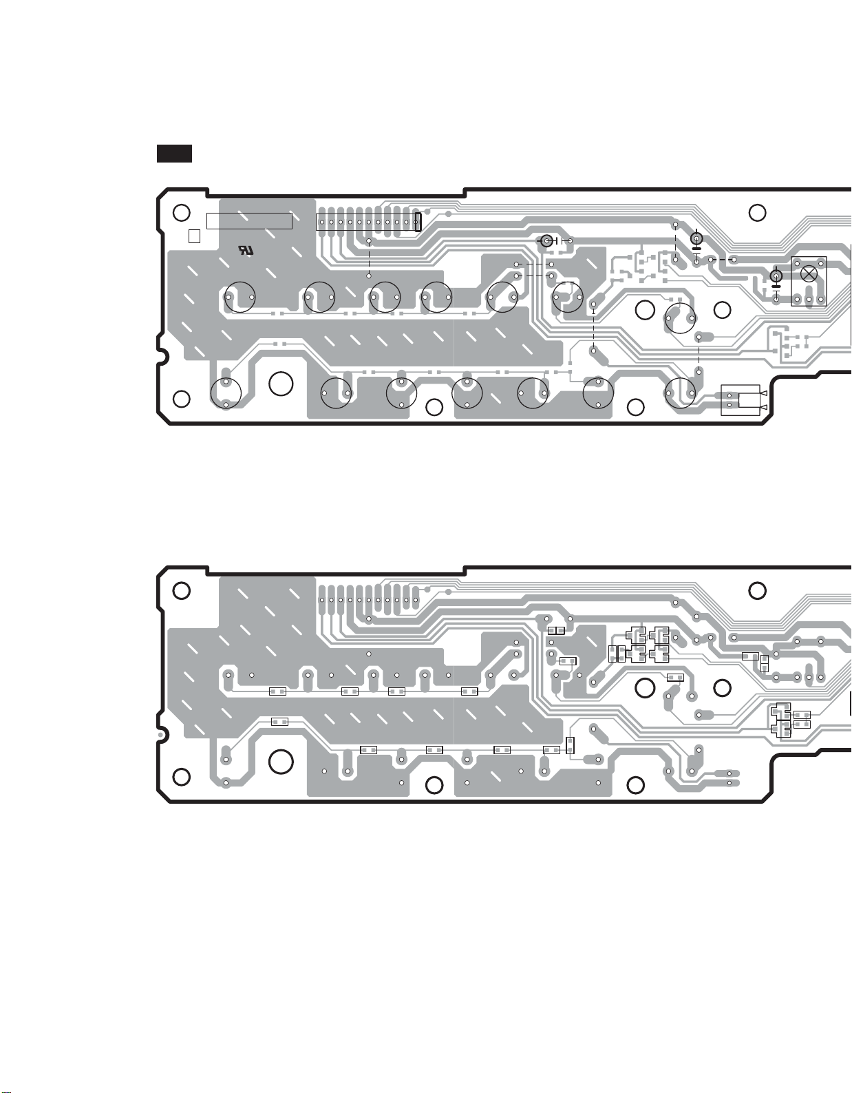
PRINTED CIRCUIT BOARD VIEW FROM SOLDERING SIDE-2
18 of 63
U20 : DISPLAY CIRCUIT PC BOARD NADIS-8054
NCDIS-8054
0
25138054A
2
S812
7
7
2
J816
J817
S808
C808
222222
S814S815S816S817S818S819
C807
R814
R808
R809R810R811R812
P752A
7
2
S811
F2
VDISP
R817R818
J818
2
S810
GND
GND
SUBRESET
SUBCL
SUBSI
SUBSO
5V
SUBREQ
R816
2
S809
R815
DISC6 DISC5 DISC4 DISC3 DISC2 DISC1
F1
R819
S807
J815
2
7
C804
J814
OPEN/CLOSE
J813
C801
VCC
VOUT
GND
Q810
2
S813
7
FRFFDOWNUPSTOPPLAY/PAUSE
Q806
R805
R806
Q807
DISC-SKIP
2
S806
Q808
Q809
R813
J812
P802B
R834
P802B
Component side
C802
R832
Q803Q804
R831
Soldering side
Page 19
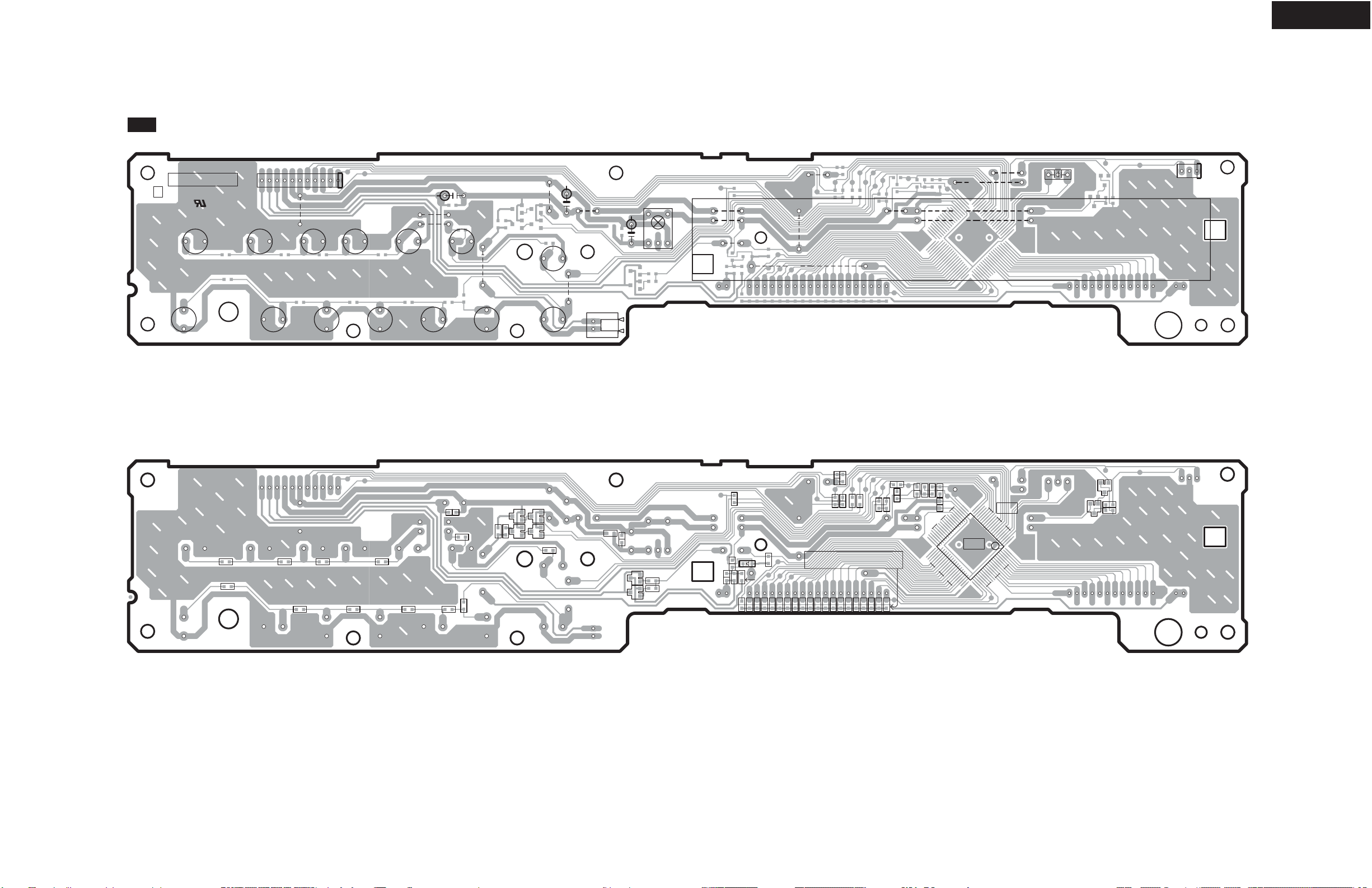
PRINTED CIRCUIT BOARD VIEW FROM SOLDERING SIDE-2
19 of 63
U20 : DISPLAY CIRCUIT PC BOARD NADIS-8054
DX-C390
NCDIS-8054
0
25138054A
2
S812
7
7
2
J816
J817
S808
C808
222222
S814S815S816S817S818S819
C807
R814
R808
R809R810R811R812
P752A
7
2
S811
F2
VDISP
R817R818
J818
2
S810
GND
GND
SUBRESET
SUBCL
SUBSI
SUBSO
5V
SUBREQ
R816
2
S809
R815
DISC6 DISC5 DISC4 DISC3 DISC2 DISC1
F1
R819
S807
J815
2
J807
7
C804
J814
OPEN/CLOSE
2
S813
FRFFDOWNUPSTOPPLAY/PAUSE
R805
Q806
R806
Q807
DISC-SKIP
2
S806
Q808
Q809
R813
7
J812
J813
P802B
R834
P802B
C802
Q803Q804
C801
R832
R831
VCC
GND
VOUT
Q810
Component side
7
7
C809
J810
J811
C810
J809
R830
R835
D804
R829
R836
30
J808
R899
R898
R897
R896
J806
C811
R895
R894
C812
R893
C813
R892
R801
R891
R802
R890
R803
R889
R888
R887
R807
R886
R885
R884
R883
R882
J805
R826
R881
R880
R837
C814
C815
R828
30
30
Q802
Q802
C816
R827
C806
40
41
6061
Q801
7
J803
17
J804
J801
J802
20 21
Q801
1
80
X801
Q805
P801A
Q811
R804
R833
Soldering side
Page 20

DX-C390
20 of 63
7
7
C809
J810
J811
C810
J809
R830
R835
D804
R829
R836
30
J808
R899
J807
R898
R897
R896
J806
C811
R895
R894
C812
R893
C813
R892
R801
R891
R802
R890
R803
R889
R888
R887
R807
R886
R885
R884
R883
R882
J805
R826
R881
R880
R837
C814
C815
R828
7
J803
17
J804
30
J801
30
J802
X801
P801A
Q802
Q802
C816
R827
C806
40
20 21
Q801
1
Q805
Q811
R804
R833
Q801
41
80
6061
Page 21

PRINTED CIRCUIT BOARD VIEW FROM SOLDERING SIDE-3
21 of 63
U23 : MECHANISM CONTROL PC BOARD NADG-8057
DX-C390
P751A
0
25138057
NCDG-8057
P705A
F1
F2
GND
B5V
MGND
VDISP
BMECHA
J613
J614
7
J616
J615
Q602
J609
P704B
P704B
Component side
J612
R613
C606
J610
Q601
C601
P701B
RST
SOCLSI
DISC-S
REQ
STOP-S
LOD-L
LOAD-2
LOD-R
CURRENT
LOAD-3
LOAD-1
ROT-L
ROT-R
ROTH
J605
J606
J603
J602
SIDE
CONTACT
P702A
7
12
J607
J604
7
P701B
7
R604
7
J611
127
J608
7
J601
S601
S603
S602
C608
R611
Q608
R607
R608
R612
D603
D604
R610
R627
R605
R606
Soldering side
R609
C607
C602
R602
R603
D602
D601
R601
Q607
R614
R615
R616
C611
R628
C609
Q606
R624
R626
R619
R621
C605
Q604
R623
R618
R617
C610
C604
R625
R622
C603
R620
Q605
Q603
Page 22

PRINTED CIRCUIT BOARD VIEW FROM SOLDERING SIDE-4
22 of 63
U26 : ROULETTE MOTOR PC BOARD NAETC-8060
P703B
+
Z701
25138060
Z701
ETC8060
U27 : LOADING MOTOR PC BOARD NAETC-8061
C655
DX-C390
Z702
1
NCETC-8061
P704A
+
25138061
Z702
U28 : CONNECTION PC BOARD
NAETC-8062
P751B
P752B
0
NCETC-806225138062
C656
P707
P706B
NCETC-8067
25138067
0
U30 : POWER SWITCH PC BOARD
NASW-8063 <MPP> <MPA> ONLY
C907
S901
NCSW-8063
25138063
0
S901
J902B J901B
Page 23

PRINTED CIRCUIT VIEW FROM SOLDERING SIDE-5
23 of 63
U21 : STANDBY LED PC BOARD NASW-8055
NCSW-8055
0
25138055
P801B
DX-C390
REPEATRANDOMDIMERDISPLAY
2222
S801
S804S803S802
Component side
R823R824R825 R822
Soldering side
U29 : ILLUMINATION PC BOARD NADIS-8066
D805
P802A
P802A
D802
D802
Component side
STANDBY/ON
2
S805
NCDIS-8066
D803
25138066
D801
0
R820
R838
R821
Soldering side
Page 24

PRINTED CIRCUIT BOARD VIEW FROM SOLDERING SIDE-6
24 of 63
U24 : POWER TRANSFORMER PC BOARD NAPS-8058
DX-C390
12
J902
F901
C901
C902
T902
C912
P902A
C917
C903
C916
OF
RISK
-REPLACE FUSE
AS MARKED
J901
T901
FIRE
125V
800mA
T901
U25 : DISC SENSOR PC BOARD NAETC-8059
NCETC-8059
P702B
Q651
0
Q651
576
25138059
Q652
F901AF901B
223OR6
P703A
T902
0
J903
J901AJ902A
AC-H
NCPS-8058
25138058
P901A
J904B
J903B
AC-H
AC-G
AC-G
C652
R651
R655R656
Component side
C653
R652
Soldering side
R654
C654
R653
Page 25

PRINTED CIRCUIT VIEW FROM SOLDERING SIDE-7
25 of 63
U22 : OUTPUT TERMINAL PC BOARD NAAR-8056
DX-C390
J107
1
P904B
15
17
J108
P705B
25138056
NCAR-8056
CDMUT
RI
P-OFF
POWER
GND
5V
GND
3.3V
SW5V
BMECHA
BMECHA
MGND
VDISP
F1
F2
GND
B5V
C915
C910
Q902
C908
D905
C913
D906
C909
R901
Q905
J114
J102
C302
C310
E901
7
C906
J109
Q901
25
J101
P102B
J115
C312
J110
12
R330
15
17
7
J116
C304
J111
C311
C303
7
C305 C306
C301
R331
C307 C308
J119
J117
J112
J118
17
12
C309
C174
7
J104
J103
C905
C904
J105
C905
D901
J106
P902B
P103B
C911
Q306
C168
J113
Q305
17
P152
Q156
P151
P151
P152
C175
Q156
C904
P153
1
Q303
R324
R322
R321
R323
R904
P153
R326
R325
L159
L153
C167
Component side
R329
R334
R327
Q307
Q903
R332
R333
L901
R908
R907
Q904
C315
D301
R328
R302
R301
R341 R342
R304
R303
R305
R306
R310
R309
R307 R308
Q302
Q301
1
1
R311
R335
R903
R902
R336
R312
R320
R319
R314
R318
R316
R315
R317
R313
D908
D907
Soldering side
D909
R148
R905
L152
C165
C166
Page 26

IC BLOCK DIAGRAM/ TERMINAL DESCRIPTION
26 of 63
Q551 : AK4103VF DIGITAL AUDIO TRANSMITTER
DX-C390
PIN LAYOUT
V1
TRANS
PDN
MCLK
SDTI
BICK
LRCK
FS0/CSN
FS1/CDTI
FS2/CCLK
FS3/CDTO
C1
PIN / FUNCTION
No. PIN NAME I/O DESCRIPTION
1 V1 I Validity bit input pin
2TRANS I
3 PDN I Power down & reset pin. When "L", the AK4103 is powered4 MCLK I Master clock input pin.
5 SDTI I Audio serial data input pin.
6 BICK I/O Audio serial data clock input/ output pin.
7 LRCK I/O Input output channel clock pin.
8 FS0 I Sampling frequency select 0 pin at synchronous mode.
9 FS1 I Sampling frequency select 1 pin at synchronous mode.
10 FS2 I Sampling frequency select 2 pin at synchronous mode.
11 FS3 I Sampling frequency select 3 pin.
12 C1 I Channel status bit input pin.
13 ANS I Asynchronous/synchronous mode select pin. 1: synchronous
14 BLS I/O Block start input/output pin.
15 CKS0 I Clock mode select 0 pin.
16 CKS1 I Clock mode select 1 pin.
17 VDD - power supply pin. 4.75 to 5.25V
18 VSS - Ground pin.
19 TXN O Negative differential output pin.
20 TXP O Positive differential output pin.
21 DIF0 I Audio serial input select 0 pin.
22 DIF1 I Audio serial input select 1 pin.
23 DIF2 I Audio serial input select 2 pin.
24 U1 I User data bit input for channel 1.
BLOCK DIAGRAM
U1
1
2
3
4
5
6
7
8
9
10
11
12
24
DIF2
23
DIF1
22
DIF0
21
TXP
2.
TXN
19
VSS
18
VDD
17
CKS1
16
CKS0
15
BLS
14
ANS
13
BICK
LRCK
SDTI
C1
U1
V1
FS0
FS1
FS2
FS3
DIF2
DIF1
DIF0
Audio Serial
Interface
MUX
Register
CKS1
CKS0
MCLK
Prescaler
Biphase
Encoder
CRC Generator
Host Serial
Interface
CSN
CDTI
CCLK
BLS
CDTO
TRANS
Audio routing mode (transparent mode) pin at synchronous mode.
0: Normal mode, 1: Audio routing mode
CSN I Host interface chip select pin at asynchronous mode.
AKMODE I AK4112A: mode pin at audio routing mode.
CDTI I Host interface data input pin at asynchronous mode.
CCLK I Host interface bit clock input pin at asynchronous mode.
CDTI O Host interface data output pin.
VSS
VDD
TXP
TXN
RS422 Line Driver
ANS
PDN
Page 27

IC BLOCK DIAGRAM/ TERMINAL DESCRIPTION
27 of 63
Q155 : TC74VHCU04FT (Hex inverter)
Block diagram
DX-C390
1A
1Y
2A
2Y
3A
3Y
GND
1
2
3
4
5
6
7
14 Vcc
13 6A
12 6Y
11 5A
10 5Y
9 4A
8 4Y
Truth table
A
Y
L
H
H
L
Page 28

IC BLOCK DIAGRAM/ TERMINAL DESCRIPTION
28 of 63
Q601, Q602 : TA7291S (MOTOR DRIVER)
BLOCK DIAGRAM
Vcc Vref
2
8
6
Vss
DX-C390
Reg.. Power
Supply
Protection
circuit
9
1
IN2
PIN FUNCTION
PIN No.
2
6
8
5
9
1
7
3
Pin 4 : NC
5
GNDIN1
SYMBOL
Vcc
VS
Vref
GND
IN1
IN2
OUT1
OUT2
7
OUT1
3
OUT2
FUNCTUIN DESCRIPTION
Supply voltage termunal for Logic.
Supply voltage terminal for Motor drive.
Supply voltage terminal for control.
GND
Input
Input
Output
Output
Truth table
INPUT OUTPUT
IN1 IN2 OUT1 OUT2
0
0
1
0
H
0
1
L
1
1
L
CW: Clockwise direction
CCW: Counter clockwise direction
L
H
L
MODE
STOP
CW/CCW
CCW/CW
BRAKE
Page 29

IC BLOCK DIAGRAM/ TERMINAL DESCRIPTION
R
W
A
A
A
Y
A
K
A
A
A
K
A
K
A
29 of 63
DX-C390
Q501 : LC78683E MP3 DECODER FOR CD
MADRS[12:0]
MDATA[15:0]
CASUB
CASLB
RASB
BLOCK DIAGRAM
CKIN
VPRF
VCOC
VPDO
CKOUT
WOK
CNTOK
OVF
LRSY
DATACK
DATAIN
C2FIN
SFSY
P
SBSY
SBCK
RESB
generator
System
clock-
VCO
PLL
CD-DA shockproof
(Compressed or
uncompressed)
WEB
OEB
DRAM-I/F
CDROM
decoder
CL
CPU-I/F
Data-I/F
MP3
decoder
M
U
X
Audio I/F
CMDOUT
CMDIN
INTB
CE
STREQ
STCK
STDAT
CRCF
FSYNC
DLRCK
DBCK
DDATA
PIN ASSIGNMENT
LRSY
DDAT
DBC
DLRC
C2FIN
TEST1
CKIN
CKOUT
TEST2
DVDD1
SBS
SFSY
SBC
VPRFR
VCOC
VPDO
VSS
PW
VDD
VSS
1
2
3
4
5
6
7
8
9
10
11
12
13
14
15
16
17
18
19
20
RESB
DATACK
DATAIN
80 79 78
21 22 23 24
VSS
DVDD2
MDATA0
CL
CMDIN
INTB
CE
77
76 75 74 73 72 71 70 69 68 67 66 65 64 63 62 61
CMDOUT
OVF
VSS
CNTOK
WOK
DVDD6
CRCF
STCK
FSYNC
STDAT
LC78684
(Top view)
25 26 27 28 29 30 31 32 33 34 35 36 37 38 39 40
VSS
MDATA1
MDATA2
MDATA3
MDATA4
MDATA5
DVDD3
MDATA7
MDATA6
MDATA8
MDATA9
MDATA12
MDATA10
MDATA11
STREQ
VSS
DVDD5
60
MADRS0
59
MADRS1
58
MADRS2
57
MADRS3
56
MADRS4
55
MADRS5
54
MADRS6
53
MADRS7
52
VSS
DVDD4
51
MADRS8
50
MADRS9
49
MADRS10
48
MADRS11
47
46
MADRS12
45
OEB
44
CASUB
43
CASLB
42
WEB
41
RASB
MDATA15
MDATA13
MDATA14
Page 30

IC BLOCK DIAGRAM/ TERMINAL DESCRIPTION
30 of 63
Q501 : LC78683E MP3 DECODER FOR CD
Pin Functions
Pin No. Pin Name I/O Block Function
1 LRSY I CD IF CD left/right clock input
2 ADDATA O Audio data output
3 ADBCK O Audio bit clock output
4 ADLRCK O
5 C2FIN I CD IF CD C2 error flag input
6 TEST1 I Test Test input 1 (This pin must be connected to ground during normal operation.)
7 CKIN I CLOCK System clock input (16.9344 MHz)
8 VSS Power supply Ground
9 CKOUT O CLOCK External digital filter and D/A converter clock (384 fs) output
10 TEST2 I Test Test input 2 (This pin must be connected to ground during normal operation.)
11 DVDD1 Power supply Digital I/O system power supply
12 PW I CD subcode data serial input
13 SBSY I CD subcode block sync si gnal input
14 SFSY I CD subcode frame sync signal input
15 SBCK O
16 AV
17 VPRFR VCO oscillator range setting
18 VCOC I VCO control voltage input
19 VPDO O
20 AVSS Analog system ground
21 DVDD2 Internal logic system power supply
22 VSS
23 MDATA0 I/O DRAM data bus 0
24 MDATA1 I/O DRAM data bus 1
25 MDATA2 I/O DRAM data bus 2
26 MDATA3 I/O DRAM data bus 3
27 MDATA4 I/O DRAM data bus 4
28 MDATA5 I/O DRAM data bus 5
29 MDATA6 I/O DRAM data bus 6
30 MDATA7 I/O
31 DVDD3 Digital I/O system power supply
32 VSS
33 MDATA8 I/O DRAM data bus 8
34 MDATA9 I/O DRAM data bus 9
35 MDATA10 I/O DRAM data bus 10
36 MDATA11 I/O DRAM data bus 11
37 MDATA12 I/O DRAM data bus 12
38 MDATA13 I/O DRAM data bus 13
39 MDATA14 I/O DRAM data bus 14
40 MDATA15 I/O DRAM data bus 15
41 RASB O RAS output (active low)
42 WEB O WE output (active low)
43 CASLB O CAS output (lower byte, active low)
44 CASUB O CAS output (upper byte, active low)
45 OEB O OE output (active low)
46 MADRS12 O DRAM address output 12
47 MADRS11 O DRAM address output 11
48 MADRS10 O DRAM address output 10
49 MADRS9 O DRAM address output 9
50 MADRS8 O
DD
Audio interface
Audio left/right clock output
Subcode interface
CD subcode transfer serial clock output
Power supply Analog system (PLL) power supply
PLL
VCO charge pump output
Analog system ground
Power supply
GND
Memory interface
DRAM data bus 7
Power supply
Memory interface
GND
DRAM address output 8
DX-C390
Continued on next page.
Page 31

IC BLOCK DIAGRAM/ TERMINAL DESCRIPTION
31 of 63
Q501 : LC78683E MP3 DECODER FOR CD
Continued from preceding page.
Pin No. Pin Name I/O Block Function
51 DVDD4 Digital I/O system power supply
52 VSS
53 MADRS7 O DRAM address output 7
54 MADRS6 O DRAM address output 6
55 MADRS5 O DRAM address output 5
56 MADRS4 O DRAM address output 4
57 MADRS3 O DRAM address output 3
58 MADRS2 O DRAM address output 2
59 MADRS1 O DRAM address output 1
60 MADRS0 O
61 DVDD5 Internal logic system power supply
62 VSS
63 STREQ I/O
64 STCK I/O
65 STDAT I/O
66 FSYNC O MP3-dec
67 CRCF O CD monitor
68 DVDD6 Digital I/O system power supply
69 VSS
70 WOK I
71 CNTOK O
72 OVF O
73 CMDOUT O Serial command data output (n-channel open-drain output)
74 CMDIN I Serial command data input
75 CL I Serial command clock input
76 CE I Command enable input (active high)
77 INTB O
78 RESB I
79 DATAIN I Serial CD data input
80 DATACK I
Notes: 1. Notes on unused pins.
Unused input pins must be connected to the ground level (0 V).
Unused output pins must be left open. Do not connect anything to these pins.
Unused I/O pins may either be connected to the ground level (0 V) or set to output mode and left open.
2. The corresponding power supply levels must be provided to all of the DV
corresponding power supply level must also be provided to DV
the supply levels.)
3. The TEST1 and TEST2 input pins must be connected to ground (0 V).
4. The I/O pins (MDAT0:15, STREQ, STCK, and STDAT) go to input mode after a reset.
5. After first applying the power supply levels, the RESB pin must be held low for at least 1 µs.
6. A 16.9344 MHz clock signal must be supplied to the CKIN pin by the CD DSP.
The LC78684E does not support the implementation of an oscillator circuit using an oscillator element.
Power supply
Memory interface
Power supply
MP3 stream I/O
Power supply
CD-DA shockproof
and MP3 I/O
Microcontroller
interface
CD IF
Ground
DRAM address output 0
GND
MP3 data request flag output (active high)
/DRAM data request flag input (CD-ROM mode, active high)
MP3 data transfer clock input
/DRAM data transfer clock output
MP3 serial data input
/DRAM serial data output
MP3 frame sync signal (active high)
/Data continuity point detection complete flag (CD-DA mode, active high)
CRC check result output (CD-ROM data/CD-DA subcode data)
/DRAM data output enable signal output (active high)
GND
DRAM write enable input (CD-DA mode, active high)
/DRAM data request flag input
Data continuity point detection complete flag (CD-DA mode, active high)
/SYNC error monitor flag (MP3 mode, active high)/DRAM serial data output
DRAM write interrupt flag (CD-DA mode, active high)
/Emphasis output flag (CD-DA and MP3 modes, active high)
/DRAM data transfer clock output
Interrupt signal output (active low)
/DRAM write interrupt flag (CD-DA mode, active high)
System reset (active low)
CD bit clock input
1, DVDD3, DVDD4, DVDD6, and AVDD pins. The
DD
2 and DVDD5. (See the Allowable Operating Ranges specifications for
DD
DX-C390
Page 32

DX-C390
32 of 63
IC BLOCK DIAGRAM/ TERMINAL DESCRIPTION
Q103 : CXD3068Q DIGITAL SIGNAL PROCESSOR-1
BLOCK DIAGRAM
71 72 69 59 60 58
27
16
50
49
48
62
57
12
53
54
55
52
25
24
23
7
4
5
6
15
79
80
78
76
77
Clock
Generator
Asymmetry
Corrector
Digital
PLL
Digital
CLV
CPU
Interface
11 13 68 10
EFM
Demodulator
Servo
Auto
Sequencer
Sub code
Processor
17 14 65 66 67 3
Error
Corrector
32K
RAM
D/A
Interface
Digital
OUT
80 pin QFP
37
36
2
63
64
73
74
Servo
Interface
MIRR
DFCT
FOK
43
42
41
40
39
38
46
OP Amp.
Analog SW
A/D
Converter
44
Servo DSP
Focus servo
Tracking servo
Sled servo
PWM Generator
Focus PWM
Generator
Tracking PWM
Generator
Sled PWM
Generator
75
8
19
26
9
20
21
22
33
34
31
32
29
30
Page 33

IC BLOCK DIAGRAM/ TERMINAL DESCRIPTION
33 of 63
Q103 : CXD3068Q DIGITAL SIGNAL PROCESSOR-2
PIN DESCRIPTION
No. SIGN I/O DESCRIPTION
1DV
2 XRST I System reset pin. L= Reset
3 MUTE I Mute input pin. H= Mute
4 DATA I Serial data input pin from CPU.
5 XLAT I Latch signal input pin from CPU.
6 CLOK I The clock input pin for transmission of serial data.
7 SENS O SENS signal output pin for CPU.
8 SCLK I The clock input for reading of serial data.
9 ATSK I/O Input/ output pin for anti-shock.
10 WFCK O WFCK output pin.
11 XUGF O XUGF output pin.
12 XPCK O XPCK output pin.
13 GFS O GFS output pin.
14 C2PO O C2PO output pin.
15 SCOR O When detected the sub code sink S0 or S1, outputting is "H".
16 C4M O 4.2336M Hz output pin.
17 WDCK O Word clock output pin. F=2Fs.
18 DV
19 COUT I/O The number of count signal input and output of tracks
20 MIRR I/O Mirror signal output/ input pin.
21 DFCT I/O Defect signal output/ input pin.
22 FOK I/O Focus OK signal output/ input pin.
23 PWM1 I Outer edge control pin of spindle motor.
24 LOCK I/O GFS is sampled by 460Hz, When GFS is "H", outputting is "H".
25 MPD O Servo control output pin for spindle motor.
26 SSTP I The detected signal input inside a disk
27 FSTO O 2/3 divided signal output pin of XTAL terminal.
28 DV
29 SFDR O Sled drive output pin.
30 SRDR O Sled drive output pin.
31 TFDR O Tracking drive output pin.
32 TRDR O Tracking drive output pin.
33 FFDR O Focus drive output pin.
34 FRDR O Focus drive output pin.
35 DV
36 TEST I Test pin. (To connect the GND)
37 TES1 I Test pin. (To connect the GND)
38 VC I Center voltage input pin.
39 FE I Focus error signal input pin.
40 SE I Sled error signal input pin.
DD0 - Di ital ower su l terminal.
SS0 - Digital ground.
When GFS is eight consecutive time "L." outputting is "L".
DD1 - Digital power supply.
SS1 - Digital GND.
DX-C390
Page 34

IC BLOCK DIAGRAM/ TERMINAL DESCRIPTION
34 of 63
Q103 : CXD3068Q DIGITAL SIGNAL PROCESSOR-3
PIN DESCRIPTION
No. SIGN I/O DESCRIPTION
41 TE I Tracking error input pin.
42 CE I Center servo analog signal input pin.
43 RFDC I RF signal input pin.
44 ADIO O Test pin.
45 AV
46 IGEN I Regulated power supply pin for OP-Amp.
47 AV
48 ASYO O EFM full swing output pin. L= V
49 ASYI I The input pin of cooperate voltage of asymmetry.
50 RFAC I EFM signal input pin.
51 AV
52 CLTV I VCO1 control voltage input pin.
53 FILO O Filter circuit output pin for master PLL.
54 FILI I Filter circuit input pin for master PLL.
55 PCO O Change pump circuit output pin for master PLL.
56 AV
57 BIAS I The constant current input of an asymmetry circuit
58 VCTL I VCO2 control voltage input pin for EFM PLL.
59 V16M I/O VCO2 osculation output pin for EMF PLL.
60 VPCO O Charge pump output pin for EMF PLL.
61 DV
62 ASYE I Select ON/OFF of asymmetry circuit. L= OFF, H= ON
63 MD2 I Digital output control pin. L= OFF, H= ON
64 DOUT O Digital output pin.
65 LRCK O D/A interface output pin. LR clock output.
66 PCMD O D/A interface output pin. Serial data output.
67 BCK O D/A interface output pin. Bit clock output.
68 EMPH O When detect the emphasis on the disc, outputting is "H".
69 XTSL I X'tal select input pin. 16.9344MHz= L, 33.8688MHz= H
70 DV
71 XTAI I Input pin for connect the crystal OSC.
72 XTAO O Output pin for connect the crystal OSC.
73 SOUT O Serial data output pin.
74 SOCK O Clock signal of reading serial data output pin.
75 XOUT O Serial latch output pin.
76 SQSO O Peak level data output pin.
77 SQCK I Clock signal output pin for SQSO read out.
78 SCSY I Input pin of GRSCOR.
79 SBSO O Serial output pin for Sub P to Sub W.
80 EXCK I Clock input pin for SBSO read out.
SS0 - Analog GND.
DD0 - Analog power supply.
SS1 - Analog GND.
DD1 - Analog power supply.
DD2 - Digital power supply.
SS2 - Digital GND.
DX-C390
SS, H= VDD
Page 35

IC BLOCK DIAGRAM/ TERMINAL DESCRIPTION
35 of 63
Q102 : CXA2851N RF SIGNAL PROCESSOR
PIN ASSIGNMENT
DC_OFST
RFDCI
RFDCOVCRFC
30
VFC
BST
RFG
Vcc
CEICETE_BALTEFEI
25
26272829
22
2324
1718
192021
16
DX-C390
FE
1
LD
2 3
PD
4 5 6
EQ_IN
AC_SUM
GND
7
A
B
Terminal Description
PIN No. PIN SIGN DESCRIPTION
1
2
3
4
5
6
7
8
9
10
11
12
13
14
15
16
17
18
19
20
21
22
23
24
25
26
27
28
29
30
LD
PD
EQ_IN
AC_SUM
GND
A
B
C
D
E
F
SW
DVcc
DVC
RFAC
DC_OFST
RFDCI
RFDCO
VC
RFC
VFC
BST
RFG
Vcc
CEI
CE
TE_BAL
TE
FEI
FE
I/O
O
O
O
O
O
O
O
O
O
Output pin for APC amp.
Input pin for APC amp.
I
Input pin for EQ block and VCA block of RFAC system.
I
Output pin for RF SUM of RF AC system.
GND pin
I
A-signal input pin.
I
B-signal input pin.
I
C-signal input pin.
I
D-signal input pin.
I
E-signal input pin.
I
F-signal input pin.
I
Mode select input pin.
I
DVcc input pin.
I
DVcc output pin.
RFAC signal output pin.
Focus error signal output pin.
Virtual grounding pin of FE Amp.
I
Tracking error signal output pin.
TE balance adjusting pin.
I
Center error signal output pin.
Virtual grounding pin of CE Amp.
I
Vcc pin.
I
AF signal gain adjusting pin of VCA block.
I
Adjust the boost quantity of EQ.
I
Adjust the cutoff frequency signal of EQ.
I
Adjust the cutoff frequency signal of EQ.
I
VC voltage output pin.
RFDC signal output pin.
Virtual grounding pin of RFDC Amp.
I
Offset adjusting output pin for RFDC.
I
8 9
C
D
10 11
E
12
14 15
13
F
SW
DVC
DVc c
RFAC
Page 36

IC BLOCK DIAGRAM/ TERMINAL DESCRIPTION
36 of 63
Q706 : BR93L56F-WE2 128 x 16 bit Electrically Programmable ROM-1
DX-C390
Page 37

IC BLOCK DIAGRAM/ TERMINAL DESCRIPTION
37 of 63
Q706 : BR93L56F-WE2 128 x 16 bit Electrically Programmable ROM-2
BLOCK DIAGRAM
DX-C390
Page 38

IC BLOCK DIAGRAN / TERMINAL DESCRIPTION
38 of 63
Q201 : BA5984FP
5ch BTL Driver
28 27 26 25 24 23 22 21 20 19 18 17 16 15
MUTE
10k
10k
DX-C390
10k
10k
10k
10k
10k
OUTF
REV
OUTR
FWD
1 2 3 4 5 6 7 8 9 10 11 12 13 14
10k
16k
16k
10k
16k
16k
LEVEL SHIFT
LEVEL SHIFT
10k
V
CC
10k
10k
10k
LEVEL SHIFT
LEVEL SHIFT
10k
10k
10k 10k
10k
10k
10k
Page 39

IC BLOCK DIAGRAN / TERMINAL DESCRIPTION
39 of 63
Q201 : BA5984FP
Terminal Description
DX-C390
Pin No.
1
2
3
4
5
6
7
8
9
10
11
12
13
14
15
16
17
18
19
20
21
22
23
24
25
26
27
28
Name
Description
Loading driver input terminal (FWD)
BTL amp. 1 input terminal (non-inverting side)
BTL amp. 1 input terminal (inverting side)
BTL amp. 1 output terminal
BTL amp. 2 input terminal (non-inverting side)
BTL amp. 2 input terminal (inverting side)
BTL amp. 2 output terminal
Power supply terminal
Loading driver output terminal (negative output)
Loading driver output terminal (positive output)
Driver CH2 output terminal (negative output)
Driver CH2 output terminal (positive output)
Driver CH1 output terminal (negative output)
Driver CH1 output terminal (positive output)
Driver CH4 output terminal (negative output)
Driver CH4 output terminal (positive output)
Driver CH3 output terminal (negative output)
Driver CH3 output terminal (positive output)
Ground terminal
BIAS signal input terminal
Muting control terminal
BTL amp. 3 output terminal
BTL amp. 3 input terminal (inverting side)
BTL amp. 3 input terminal (non-inverting side)
BTL amp. 4 output terminal
BTL amp. 4 input terminal (inverting side)
BTL amp. 4 input terminal (non-inverting side)
Loading driver input terminal (REV side)
Page 40

IC BLOCK DIAGRAM/ TERMINAL DESCRIPTION
40 of 63
Q154 : UPC29L00 SERIES
THREE TERMINAL VOLTAGE REGULATOR
DX-C390
CONNECTION DIAGRAM
uPC29L00J Series
123
Output
GND
Input
uPC29L00TSeries
123
Output
GND
GND
Input
BLOCK DIAGRAM
Startup circuit
Reference voltage
Thermal shut down
Error
Amp.
Over-current
protection
Driver circuit
INPUT
OUTPUT
GND
Page 41

FL TUBE VIEW
MP3
REMAIN
TOTAL
NAME
A - B
TRACK
NEXT
FLDR
SACD
DISC
REPEAT
MEMORY
RANDOM
MP3
REMAIN
TOTAL
NAME
A -
TRACK
NEXT
FLDR
SACD
DISC
REPEAT
MEMORY
RANDOM
41 of 63
Q802: HNV-12SM57
GRID ASSIGNMENT
1G 2G 3G 4G 5G 6G 7G 8G 9G 10G 11G 12G
DISC
REPEAT
MEMORY
RANDOM
PIN CONNECTION
SACD
f
e
FLDR
j
h
g
r
p
d
(2G-11G)
DX-C390
NEXT
a
b
k
m
n
c
TRACK
A - B
NAME
Col
TOTAL
REMAIN
Col
MP3
1 2
4
3
5
6
PIN No.
CONNECTION
1F12F13NP4NP51G62G73G84G95G106G117G128G139G14
ANODE CONNECTION
P1
P2
P3
P4
P5
P6
P7
P8
P9
P10
P11
P12
P13
P14
P15
P16
P17
P18
1G
a
j
h
k
b
f
g
m
c
e
n
r
p
d
DISC
REPEAT
MEMORY
RANDOM
2G
a
j
h
k
b
f
g
m
c
e
n
r
p
d
SACD
P19
3G
a
j
h
k
b
f
g
m
c
e
n
r
p
d
FLDR
4G
a
j
h
k
b
f
g
m
c
e
n
r
p
d
NEXT
10G1511G1612G
5G
a
j
h
k
b
f
g
m
c
e
n
r
p
d
17-39NX40P141P242P343P444P545P646P747P848P949
6G
a
j
h
k
b
f
g
m
c
e
n
r
p
d
TRACK
7G
a
j
h
k
b
f
g
m
c
e
n
r
p
d
A -
B
8G
a
j
h
k
b
f
g
m
c
e
n
r
p
d
NAME
Col
P1050P1151P1252P1353P1454P1555P1656P1757P1858P1959NP60NP61F262F2
1) Fn : Filament pin
2) nG : Grid pin
3) Pn : Anode pin
4) NP : No Pin
5) NX : No exteded Pin
9G
a
j
h
k
b
f
g
m
c
e
n
r
p
d
TOTAL
10G
a
j
h
k
b
f
g
m
c
e
n
r
p
d
REMAIN
Col
11G
a
j
h
k
b
f
g
m
c
e
n
r
p
d
Col
12G
1
2
3
4
5
6
MP3
(1)
(2)
(3)
(4)
(5)
(6)
Page 42

DX-C390
S
42 of 63
MAIN MICROPROCESSOR TERMINAL DESCRIPTION-1
Q701 : uPD784225GC
No. PIN NAME SIGNAL NAME I/O DESCRIPTION
1 P15/ANI5 GND I Not used. To connect GND pin.
2 P16/ANI6 GND I Not used. To connect GND pin.
3 P17/ANI7 GND I Not used. To connect GND pin.
4 AVss GND I GND
5 P130/ANO0 O Not used. Open pin.
6 P131/ANO1 O Not used. Open pin.
7 AVref1 +5V I Power supply pin for A/D port.
8 P70/SI2/RxD2 RXD I Received pin of RS232C mode.
9 P71/SO2/TxD2 TXD O Output pin of RS232C mode
10 P72/~SCK2/ASCK2 GND I Not used. To connect GND pin.
11 P20/SI1/RxD1 MSI I Data input pin from MP3 decoder and sub code data form CD processor.
12 P21/SO1/TxD1 MSO O Transmitting data output pin to MP3 decoder and command data of CD processor.
13 P22/~SCK1/ASCK1 MSCK O Decoder clock output pin. Communicate to MP3 decoder.
14 P23/PCL DOUT O Select the CD or MP3 output mode. L=MP3 H=CD
15 P24/BUZ SUBRST O Reset signal output pin.
16 P25/SI0/SDA0 SUBSO I Serial data input pin from sub microprocessor.
17 P26/SO0 SUBSI O Serial data output pin to sub microprocessor.
18 P27/~SCK0/SCL0 SUBCL O Serial clock output pin to sub microprocessor.
19 P40/AD0 CDSUBQ O Select the CD sub code output pin of serial port.
20 P41/AD1 CDCOM O Select the CD command output pin of serial port.
21 P42/AD2 MP3COM O Select the MP3 decoder output pin.
22 P43/AD3 MP3CE O Chip enable signal output pin of MP3 decoder.
23 P44/AD4 SENSI I Sens input pin for CD signal processor.
24 P45/AD5 CDXLT O Command latch output pin for CD signal processor.
25 P46/AD6 SCLKO O Sens reading clock output terminal to CD signal processor.
26 P47/AD7 FOKI I FOK signal input pin from signal processor.
27 P50/A8 LDON O Laser light control output pin. HiZ=OFF L=CD H=CD-RW
28 P51/A9 CDRESET O Reset pin of MP3 decoder.
29 P52/A10 CDPOWER O Power supply control pin.
30 P53/A11 CDMUT O Analog mute pin. H=OFF/L=ON
31 P54/A12 STOP_POS_SEN
32 P55/A13 DISC_SENS I Disk existence detection optical sensor input terminal.
33 Vss1 GND I
34 P56/A14 ROT_R O Roulette motor control pin-R.
35 P57/A15 ROT_L O Roulette motor control pin-L.
36 P60/A16 ROTHI O Roulette motor speed control terminal..
37 P61/A17 LOADING_SW1 I Loading clamp position detection switch input terminal 1.
38 P62/A18 LOADING_SW2 I Loading clamp position detection switch input terminal 2.
39 P63/A19 LOADING_SW3 I Loading clamp position detection switch input terminal 3.
40 P64/~RD CURRENT I Loading clamp motor current detection input terminal.
41 P65/~WR LOADING_L O Loading clamp motor control terminal L.
42 P66/~WAIT LOADING_R O Loading clamp motor control terminal R.
43 P67/ASTB O Not used. Open pin.
44 P30/TO0 O Not used. Open pin.
45 P31/TO1 DITDI I The serial transmission data input terminal to DIT.
46 P32/TO2 DITDO O The serial transmission data output terminal to DIT.
47 P33/TI1 DITCL O The serial data transmission data output terminal to DIT.
48 P34/TI2 DITCE O The control command chip enable signal output terminal of DIT.
49 P35/TIO0 DITPD O DIT power down signal output terminal.
50 P36/TIO1 EEPROMCS O Chip select signal output pin of EEPROM.
51 P37/EXA EEPROMCLK O Serial clock signal output pin of EEPROM.
52 P120/RTP0 EEPROMDI O Serial data signal output pin to EEPROM.
53 P121/RTP1 EEPROMDO I Serial data signal input pin from EEPROM.
54 P122/RTP2 DACMUT O Digital mute signal of DAC. H=ON/L=OFF
I Detection the sensor input pin for disc position.
GND
80 pin QFP
Page 43

MAIN MICROPROCESSOR TERMINAL DESCRIPTION-2
L
43 of 63
Q701 : uPD784225GC
No. PIN NAME SIGNAL NAME I/O DESCRIPTION
55 P123/RTP3 DACEMPHASYS O The de-emphasis control terminal of DAC. H=De-emphasis ON/L=OFF
56 P124/RTP4 O Not used. Open pin.
57 P125/RTP5 O Not used. Open pin.
58 P126/RTP6 SYSIN I RI system code input pin.
59 P127/RTP7 SYSOUT O RI system code output pin.
60 ~RESET RESET Reset pin of microprocessor.
61 P00/INTP0 EXIRIN I External IR input pin.
62 P01/INTP1 POFF I Power failure detection terminal. L=Power failure
63 P02/INTP2/NMI MP3INTB I The interruption signal input terminal from MP3 decode.
64 P03/INTP3 SCORI I The sub code detection terminal of the signal processing IC.
65 P04/INTP4 SUBREQ I The communication ready signal input terminal from sub microprocessor.
66 P05/INTP5 MP3FSYNC I FSYNC signal input pin from MP3 decoder.
67 Vss0 GND I GND
68 Vdd1 +5V I Power supply pin.
69 X2 CLOCK O Clock signal output pin. (12.5MHz OSCO)
70 X1 CLOCK I Clock signal input pin. (12.5MHz OSC)
71 TEST/Vpp GND I Flash ROM write-in voltage pin.
72 XT2 O Not used. Open pin.
73 XT1 GND I Not used. To connect GND pin.
74 Vdd0 +5V I Power supply pin.
75 AVdd +5V I Power supply pin for A/D port.
76 P10/ANI0 MODEL I Model name select pin. 0V=DX-C390/+5V=Other model
77 P11/ANI1 TIMING I The brake timing setting terminal of roulette. (0V=0msec
78 P12/ANI2 GND I Not used. To connect GND pin.
79 P13/ANI3 GND I Not used. To connect GND pin.
80 P14/ANI4 GND I Not used. To connect GND pin.
DX-C390
+5V=64msec)
PIN LAYOUT
SUBRST
~CDCOM
GND
GND
GND
GND
+5V
RXD
TXD
GND
MSI
MSO
~MSCK
DOUT
SUBSO
SUBSI
SUBCL
CDSUB
GND
GND
GND
TIMING
MODEL
+5V
+5V
GND
GND
CLOCK
CLOCK
+5V
GND
MP3FSYNC
SUBREQ
SCORI
<--
<--
<--
<--
<--
<--
<--
<--
-->
<--
<--
-->
<--
<--
<--
<--
Vss0
P56/A14
P57/A15
-->
-->
~ROT_R
~ROT_L
P05/INTP5
P60/A16
-->
~ROTHI
P04/INTP4
P61/A17
<--
LOADING_SW1
<--
P03/INTP3
80797877767574737271706968676665646362
Vdd0
P14/ANI4
P13/ANI3
1
P15/ANI5 ~RESET
-->
2
P16/ANI6 P127/RTP7
-->
3
P17/ANI7 P126/RTP6
-->
4
AVss P125/RTP5
-->
5
P130/ANO0 P124/RTP4
<--
6
P131/ANO1 P123/RTP3
<--
7
AVref1 P122/RTP2
-->
8
P70/SI2/RxD2 P121/RTP1
-->
9
P71/SO2/TxD2 P120/RTP0
<--
10
P72/~SCK2/ASCK2 P37/EXA
-->
11
P20/SI1/RxD1 P36/TIO1
-->
12
P21/SO1/TxD1 P35/TIO0
<--
13
P22/~SCK1/ASCK1 P34/TI2
<--
14
P23/PCL P33/TI1
<--
15
P24/BUZ P32/TO2
<--
16
P25/SI0/SDA0 P31/TO1
-->
17
P26/SO0 P30/TO0
<--
18
P27/~SCK0/SCL0 P67/ASTB
<--
19
P40/AD0 P66/~WAIT
Q
<--
20
P41/AD1 P65/ ~WR
<--
P42/AD2
P43/AD3
21222324252627282930313233343536373839
-->
-->
~MP3COM
~MP3CE
AVdd
P12/ANI2
P11/ANI1
P10/ANI0
uPD784225GC
P44/AD4
P45/AD5
P46/AD6
P47/AD7
P50/A8
<--
-->
-->
<--
-->
SENSI
~CDXLT
SCLKO
FOKI
LDON
XT1
P51/A9
-->
~CDRESET
XT2
P52/A10
-->
CDPOWE R
TEST/V pp
P53/A11
-->
CDMUT
X1
P54/A12
<--
STOP POS SENSDISC_SENS
X2
P55/A13
<--
Vdd1
V ss1
<--
GND
~MP3INTB
<--
P02/INTP2/NMI
P62/A18
<--
LOADING_SW2
~POFF
<--
P01/INTP1
P63/A19
<--
LOADING_SW3
~EXIRIN
<--
61
P00/INTP0
60
~RESET
---
59
~SYSOUT
-->
58
SYSIN
<--
57
-->
56
-->
55
DACEMPHASYS
-->
54
DACMUT
-->
53
EEPROMDO
<--
52
EEPROMDI
-->
51
EEPROMCLK
-->
50
EEPROMCS
-->
49
~DITPD
-->
48
DITCE
-->
47
DITCL
-->
46
DITDO
-->
45
DITDI
<--
44
-->
43
-->
42
~LOADINGR
-->
41
~LOADING
-->
P64/~ RD
40
<--
~CURRENT
Page 44

SUB MICROPROCESSOR TERMINAL DESCRIPTION-1
44 of 63
Q801 : uPD780232GC
No. PIN NAME SIGNAL NAME I/O DESCRIPTION
1 VDD1 +5V I Power supply pin. (To connect +5V)
2 VSS1 GND I GND pin.
3 X1 CLOCK I Connect a clock OSC pin for main system.
4 X2 CLOCK O Connect a clock OSC pin for main system.
5 IC GND I Internal connect pin.
6 ~RESET ~SUBRST I Reset signal input pin from main processor.
7 P27/~SCK1 SUBCL I Communication to main microprocessor and
clock input pin for write the flash microprocessor.
8 P26/SI1 SUBSI I Data input pin for write the flash microprocessor.
9 P25/SO1 SUBSO O Data output pin for write the flash microprocessor.
10 P24/BUSY SUBREQ O Communication require output pin of a main microcomputer.
11 P23 GND I Not used. To connect GND.
12 P22 GND I Not used. To connect GND.
13 P21/SO3 STANDBYLED O Standby LED control output pin. H=Lighting, L=Light out
14 P20/~SCK3 TRAYLED1 O Tray lighting LED control terminal 1.H=Lighting, L=Light out
15 P00/INTP0 ~IRIN I Remote control signal input pin.
16 P01/INTP1 TRAYLED2 O Tray illumination LED control pin 2.
17 P02/TI O Not used. Open pin.
18 AVSS GND GND pin for A/D converter.
19 ANI3 K3 I Key input pin.
20 ANI2 K2 I Key input pin.
21 ANI1 K1 I Key input pin.
22 ANI0 K0 I Key input pin.
23 VSS0 GND I GND pin.
24 AVDD +5V I Power supply pin for A/D converter.
25 VDD0 +5V I Power supply pin. (To connect +5V)
26 P64/FIP52 FLON O Filament power supply control pin.
27 P63/FIP51 O Not used. Open pin.
28 P62/FIP50 O Not used. Open pin.
29 P61/FIP49 O Not used. Open pin.
30 P60/FIP48 O Not used. Open pin.
31 P57/FIP47 O Not used. Open pin.
32 P56/FIP46 O Not used. Open pin.
33 P55/FIP45 O Not used. Open pin.
34 P54/FIP44 O Not used. Open pin.
35 P53/FIP43 O Not used. Open pin.
36 P52/FIP42 O Not used. Open pin.
37 P51/FIP41 O Not used. Open pin.
38 P50/FIP40 O Not used. Open pin.
39 P47/FIP39 O Not used. Open pin.
40 P46/FIP38 O Not used. Open pin.
41 P45/FIP37 O Not used. Open pin.
42 P44/FIP36 O Not used. Open pin.
43 P43/FIP35 O Not used. Open pin.
44 P42/FIP34 P19 O FL tube segment output pin 19.
45 P41/FIP33 P18 O FL tube segment output pin 18.
46 P40/FIP32 P17 O FL tube segment output pin 17.
47 P37/FIP31 P16 O FL tube segment output pin 16.
48 P36/FIP30 P15 O FL tube segment output pin 15.
49 P35/FIP29 P14 O FL tube segment output pin 14.
50 P34/FIP28 P13 O FL tube segment output pin 13.
51 P33/FIP27 P12 O FL tube segment output pin 12.
52 P32/FIP26 P11 O FL tube segment output pin 11.
53 P31/FIP25 P10 O FL tube segment output pin 10.
H=ON/L=OFF
DX-C390
Page 45

SUB MICROPROCESSOR TERMINAL DESCRIPTION-2
45 of 63
Q801 : uPD780232GC
No. PIN NAME SIGNAL NAME I/O DESCRIPTION
54 P30/FIP24 P9 O FL tube segment output pin 9.
55 FIP23 P8 O FL tube segment output pin 8.
56 FIP22 P7 O FL tube segment output pin 7.
57 FIP21 P6 O FL tube segment output pin 6.
58 FIP20 P5 O FL tube segment output pin 5.
59 VDD2 +5V Power supply pin. (To connect +5V)
60 VLOAD -Vdisp Negative power supply pin.
61 FIP19 P4 O FL tube segment output pin 4.
62 FIP18 P3 O FL tube segment output pin 3.
63 FIP17 P2 O FL tube segment output pin 2.
64 FIP16 P1 O FL tube segment output pin 1.
65 FIP15 O Not used. Open pin.
66 FIP14 O Not used. Open pin.
67 FIP13 O Not used. Open pin.
68 FIP12 O Not used. Open pin.
69 FIP11 12G O FL tube grid output pin 12.
70 FIP10 11G O FL tube grid output pin 11.
71 FIP9 10G O FL tube grid output pin 10.
72 FIP8 9G O FL tube grid output pin 9.
73 FIP7 8G O FL tube grid output pin 8.
74 FIP6 7G O FL tube grid output pin 7.
75 FIP5 6G O FL tube grid output pin 6.
76 FIP4 5G O FL tube grid output pin 5.
77 FIP3 4G O FL tube grid output pin 4.
78 FIP2 3G O FL tube grid output pin 3.
79 FIP1 2G O FL tube grid output pin 2.
80 FIP0 1G O FL tube grid output pin 1.
DX-C390
Page 46

I
n
s
t
r
u
c
t
i
o
n
M
a
n
u
a
l
I
n
s
t
r
u
c
t
i
o
n
M
a
n
u
a
l
I
n
s
t
r
u
c
t
i
o
n
M
a
n
u
a
l
PACKING VIEW
L
46 of 63
DX-C390
653
604
811
En
U3DeNISv
U3FrEsIt
DX-C390
I
n
s
t
r
u
c
t
i
o
n
M
a
n
u
a
l
DX-C390
I
n
s
t
r
u
c
t
i
o
n
M
a
n
u
a
l
DX-C390
I
n
s
t
r
u
c
t
i
o
n
M
a
n
u
a
l
812
803
813
652
Cellophane tape
605
607
801
802
804
Cellophane tape
701
603a
601
R
603b
Front side
RR
610
A603a
R
DX-C390(B)
651
F
Page 47

EXPLODED VIEW PARTS LIST
47 of 63
! : Safety parts
PART NAME PART NO. DESCRIPTION REMARK
A1 F BRACKET 4154-7201-1
A1 F BRACKET 4154-7202-1
A3 CLEAR PLT 3716-9611-0
A3 CLEAR PLT 3716-9612-0
A4 SHEET 3000-9707-1 (F)
A7 BRACKET 4135-4031-1 (F)
A9 CLIP 4135-3291-0 CS-1U
A16 CHASSIS 1404-7611-1
A18 HOLDER 27190428A KGLS-10RT
A19 CUSHION 4157-0571-0
A20 WS CLAMP 27300243 CLAMP WS-2W
A24 BUSHING
A29 SCREW 830440069 4TTC+6C(BC)
A12 SCREW 838130088 3TTB+8B
A37 SCREW 831430088 3TTW+8B(BC)
A103 SCREW 838430088 3TTB+8B(BC)
A41 LEG 27175316C LEG
A42 CUSHION 28141529
A51 DOOR 4154-6121-2 (TRAY)
A51 DOOR 4154-6122-2 (TRAY) <S>
A54 SHEET 4157-0551-0 (BUTYL)t0.75x20x20
A55 SHEET 4157-0561-0 (BUTYL)
A60 LABEL 3000-9670-0
A101 REAR PANEL 1405-0802-0
A101 REAR PANEL 1405-0801-0
A121 HOLDER 27190011 KGLS-6S
A122 SCREW 838130088 3TTB+8B <MPP,MPA>
A201 FACET 3716-9806-0 (S)
A205 FACET 3716-9706-0 (LIGHT)
A208 BADGE 28135244
A208 BADGE 28135245
A221 COVER 1404-9401-0
A221 COVER 1404-9402-0
A222 SCREW 838430088 3TTB+8B(BC)
A222 SCREW 838930088 3TTB+8B(UN) <S>
A301 F PANEL 1405-0702-0
A301 F PANEL 1405-0701-0
A301 F PANEL 1405-0703-0
A311 KNOB 2446-6401-1 (POW)
A311 KNOB 2446-6402-1 (POW) <S MPP>
A313 JOINT 4154-7171-0 (POW) <MPP> <MPA>
E101 WIRE TIE 260208 CLAMPER, UL
P101 FFC 7012-6673-0 NCFC2-162512
P102 SOCKET AS 7012-6674-0 NSAS-6P1223
P103 SOCKET AS 7012-6671-0 NSAS-10P1224
P201 SOCKET AS 7012-6672-0 NSAS-12P1225
P701 FFC 7012-6670-0 NCFC5-172012
P702 FFC 7012-6522-0 NCFC6-063012
P901 AC CORD
P901 or AC CORD
P901 AC CORD
P901 or AC CORD
P901 AC CORD
P901 or AC CORD
P901 or AC CORD
P904 SOCKET AS 7012-6711-0 NSAS-20P1240
T901 P TRANS
T901 P TRANS
27300750 S-RELIEF #2271
!
253197HIT AS-SAA
!
253307VOL AS-SAA <MPA>
!
253335HIT AS-CEE <MPP>
!
253336VOL AS-CEE <MPP>
!
253333VOL AS-UC-2 <MDD>
!
253332HIT AS-UC-2 <MDD>
!
253365LON AS-UC-2 <MDD>
!
1806-3690-0 NPT-1480P
!
1806-3861-0 NPT-1480D <MDD>
!
<B>
<S>
<B>
<S>
<B>
<MPA,MPP>
<MDD>
<MPP,MPA>
<B>
<S>
<B>
<S>
<B>
<B MPP, B MPA>
<B MDD>
<S MPP>
<B MPP, B MPA>
<MPA>
<MPP,MPA>
Page 48

U10 Main circuit PC board ass'y SVC-Q0130C-MAINA NADG-8053-1A <MDD>
48 of 63
U10 Main circuit PC board ass'y SVC-Q0130C-MAINB NADG-8053-1B <MPP,MPA>
U20 Display circuit PC board ass'y SVC-Q0130C-KEY NADIS-8054-1A <MDD>
U20 Display circuit PC board ass'y SVC-Q0131C-KEY NADIS-8054-1B <MPP,MPA>
U20-1 Display circuit PC board ass'y 1H510554-1A NADIS-8054-1A <MDD>
U20-1 Display circuit PC board ass'y 1H510554-1B NADIS-8054-1B <MPP,MPA>
U21 Standby LED PC board ass'y 1H510555-1A NADIS-8055-1A <MDD>
U21 Standby LED PC board ass'y 1H510555-1B NADIS-8055-1B <MPP,MPA>
U22 Output terminal PC board ass'y 1H510556-1A NAAR-8056-1A <MDD>
U22 Output terminal PC board ass'y 1H510556-1B NAAR-8056-1B <MPP,MPA>
U23 Mechanism control PC board ass'y 1H510557-1A NADG-8057-1A <MDD>
U23 Mechanism control PC board ass'y 1H510557-1B NADG-8057-1B <MPP,MPA>
U24 Power transformer PC board ass'y 1H510558-1A NAPS-8058-1A <MDD>
U24 Power transformer PC board ass'y 1H510558-1B NAPS-8058-1B <MPP,MPA>
U25 Disc sensor PC board ass'y 1H510559-1A NAETC-8059-1A <MDD>
U25 Disc sensor PC board ass'y 1H510559-1B NAETC-8059-1B <MPP,MPA>
U26 Roulette motor PC board ass'y 1H510560-1A NAETC-8060-1A <MDD>
U26 Roulette motor PC board ass'y 1H510560-1B NAETC-8060-1B <MPP,MPA>
U27 Loading motor PC board ass'y 1H510561-1A NAETC-8061-1A <MDD>
U27 Loading motor PC board ass'y 1H510561-1B NAETC-8061-1B <MPP,MPA>
U28 Connection PC board 1H510562-1A NAETC-8062-1A <MDD>
U28 Connection PC board 1H510562-1B NAETC-8062-1B <MPP,MPA>
U29 Illumination PC board ass'y 1H510566-1A NADIS-8066-1A <MDD>
U29 Illumination PC board ass'y 1H510566-1B NADIS-8066-1B <MPP,MPA>
U30 Power switch PC board ass'y 1H510563-1B NASW-8063-1B <MPP,MPA>
PACKING PARTS LIST
REF. NO. PART NAME PART NO. DESCRIPTION REMARK
601 CARTON 1436-5501-0-2
601 CARTON 1436-5501-0-2
603a PAD 1490-4291-0 (L)
603b PAD 1490-4301-1 (R)
604 SHEET 4154-6221-0 (DR)
605 SHEET 29095949
607 POLY BAG 29100141A 700*600
610 PP TAPE 29110148 W48 OPP TAPE
651 EAN LABEL 3000-9834-0
651 UPC LABEL 3000-9836-0
651 EAN LABEL 3000-9835-0
652 WRNTY CARD 29365042
652 WRNTY CARD 29365090A
653 INST SHEET 29355299 (PAC)
701 POLY BAG 29100097-1A 350*250
801 CORD AS 2010381 PIN CORD AS
801 or CORD AS 2010326 PIN CORD AS
802 PLUG CORD 2010200 3.5-MINI PLUG (RI)
803 REMO CON 8912-0044-0 RC-547C
804 BATTERY 3010054 R6/AA(UM-3)
811 INS MANUAL 4301-7083-0 En
812 INS MANUAL 4301-7084-0 U3DeNlSv <MPP>
813 INS MANUAL 4301-7085-0 U3FrEsIt <MPP>
<B>
<S>
<B MPP, B MPA>
<B MDD>
<S MPP>
<B MPA>
<B MDD>
<B MDD>
<MPP,MPA,MDD>
CHANGER MECHANISM PARTS LIST
REF. NO. PART NAME PART NO. DESCRIPTION REMARK
M1 RAIL 4154-6031-1
M5 LODING MOTOR AS SVCQ0090CMOTCC M2+M3
(M2) MOTOR (8913-6002-1) CCM07B-045R1-1
Page 49

(M3) PULLEY (4154-6001-0)
49 of 63
M4 SCREW 833126047 2.6TTP+4S
M6 RBR BELT 4157-0281-0 DVCP701
M7 GEAR 4154-6061-0 (PULLEY)
M8 GEAR 4154-6091-0 (A)
M9 GEAR 4154-6071-0 (MAIN)
M10 GEAR 4154-6101-0 (CAM)
M11 SCREW 4135-3301-0 SCREW
M12 MECHA UNIT 24800017 KSM-213CCM
M13 CHASSIS 4154-6041-0 (SUB)
M14 INSULATOR 4154-7211-0 (CDC-A)
M16 SPRING 2510-3661-1 (CDC-A)
M17 SPRING 2510-3671-1 (CDC-B)
M18 SCREW 24840111 SCREW
M19 CAP 4154-6161-0 (CHC)
M20 YOKE 4135-3201-1 (CHB)
M21 MAGNET 4135-3211-0 (CHB)
M23 CUSHION 4157-0571-0
M24 SPRING 2510-3591-0 (DV-CP701)
M25 RETAINER 4135-4121-1 (A)
M30 TRAY 4154-6011-3
M31 BRACKET AS 8901-4650-0 (M)
M31a BRACKET 8901-4650-0 (M)
M31b SHAFT 24828038 (M)
M30 ROULETTE MOTOR AS SVCQ0090CMOTPW
(M32) (MOTOR) (8913-6003-0) PWN10EA02D
(M33) GEAR (4154-6081-0) (WORM)
M34 SCREW 82142003 2P+3F(BC)
M35 GEAR 4154-5991-0 (WHEEL)
M36 WASHER 24834040 (B)
M37 SCREW 838130088 3TTB+8B
M38 ROLLER 4154-6131-0 DVCP701
M39 ROULETTE 4154-6021-0
M40 SCREW 24840111 SCREW
M41 TAPE 29110082-1 CLOTH-8U
M50 ARM 4154-6051-0
M51 CUSHION 4157-0681-0
M52 RETAINER 4135-3881-0
M53 SCREW 838130088 3TTB+8B
M54 CUSHION 4157-0591-0
Page 50

PRINTED CIRCUIT BOARD PARTS LIST
50 of 63
DG8053
DG8053
DG8053
DG8053
DG8053
DG8053
DG8053
DG8053
DG8053
DG8053
DG8053
DG8053
DG8053
DG8053
DG8053
DG8053
DG8053
DG8053
DG8053
DG8053
DG8053
DG8053
DG8053
DG8053
DG8053
DG8053
DG8053
DG8053
DG8053
DG8053
DG8053
DG8053
DG8053
DG8053
DG8053
DG8053
DG8053
DG8053
DG8053
DG8053
DG8053
DG8053
DG8053
DG8053
DG8053
DG8053
DG8053
DG8053
DG8053
DG8053
DG8053
DG8053
DG8053
DG8053
DG8053
DG8053
DG8053
DG8053
DG8053
DG8053
DG8053
DG8053
DG8053
U10 : MAIN CIRCUIT PC BOARD NADG-8053
!: Sefety parts
CIRCUIT NO. PART NAME PART NO. DESCRIPTION REMARK
C101 CHIP ELECT C 356721019R2 CEWX6.3V-100M
C102 C-CERA C 332121045R1 CK725B1C-104K1
C103 C-CERA C 332103325R1 CK725B1H-332K1
C104 CHIP ELECT C 356723319R2 CEWX6.3V-330M
C105 C-CERA C 332161040R1 CK725F1E-104Z1
C106 CHIP ELECT C 356741009R2 CEWX16V-10M
C107 C-CERA C 332161040R1 CK725F1E-104Z1
C108 CHIP ELECT C 356721019R2 CEWX6.3V-100M
C109 C-CERA C 332161040R1 CK725F1E-104Z1
C110 C-CERA C 332104735R1 CK725B1H-473K1
C111 C-CERA C 332161040R1 CK725F1E-104Z1
C112 C-CERA C 332161040R1 CK725F1E-104Z1
C113 C-CERA C 342102214R1 CC725CH1H-221J1
C114 C-CERA C 332121045R1 CK725B1C-104K1
C115 C-CERA C 342104714R1 CC725CH1H-471J1
C117 CHIP ELECT C 356784799R2 CEWX50V-0.47M
C118 C-CERA C 332101035R1 CK725B1H-103K1
C119 C-CERA C 342102214R1 CC725CH1H-221J1
C120 C-CERA C 332101525R1 CK725B1H-152K1
C121 C-CERA C 332104735R1 CK725B1H-473K1
C122 C-CERA C 332161040R1 CK725F1E-104Z1
C123 CHIP ELECT C 356723319R2 CEWX6.3V-330M
C124 C-CERA C 332161040R1 CK725F1E-104Z1
C125 C-CERA C 332161040R1 CK725F1E-104Z1
C126 C-CERA C 332161040R1 CK725F1E-104Z1
C129 CHIP ELECT C 356722219R2 CEWX6.3V-220M
C130 C-CERA C 332161040R1 CK725F1E-104Z1
C131 CHIP ELECT C 356723319R2 CEWX6.3V-330M
C151 C-CERA C 342101504R1 CC725CH1H-150J1
C152 C-CERA C 342101804R1 CC725CH1H-180J1
C157 CHIP ELECT C 356724709R2 CEWX6.3V-47M
C159 CHIP ELECT C 356722219R2 CEWX6.3V-220M
C164 C-CERA C 332161040R1 CK725F1E-104Z1
C170 C-CERA C 332161040R1 CK725F1E-104Z1
C172 C-CERA C 332172240R1 CK725F1C-224Z1
C201 C-CERA C 332103335R1 CK725B1H-333K1
C202 C-CERA C 332103335R1 CK725B1H-333K1
C203 C-CERA C 332101035R1 CK725B1H-103K1
C204 C-CERA C 332101225R1 CK725B1H-122K1
C205 C-CERA C 332101225R1 CK725B1H-122K1
C206 C-CERA C 342106814R1 CC725CH1H-681J1
C207 C-CERA C 342106814R1 CC725CH1H-681J1
C210 CHIP ELECT C 356723319R2 CEWX6.3V-330M
C501 C-CERA C 332161040R1 CK725F1E-104Z1
C502 CHIP ELECT C 356722219R2 CEWX6.3V-220M
C503 C-CERA C 332161040R1 CK725F1E-104Z1
C504 C-CERA C 342103304R1 CC725CH1H-330J1
C505 C-CERA C 332181050R1 CK725F1A-105Z1
C506 C-CERA C 332161040R1 CK725F1E-104Z1
C507 C-CERA C 332161040R1 CK725F1E-104Z1
C508 C-CERA C 332161040R1 CK725F1E-104Z1
C509 C-CERA C 332161040R1 CK725F1E-104Z1
C510 C-CERA C 332161040R1 CK725F1E-104Z1
C511 C-CERA C 332161040R1 CK725F1E-104Z1
C512 C-CERA C 332104735R1 CK725B1H-473K1
C513 CHIP ELECT C 356722219R2 CEWX6.3V-220M
C514 C-CERA C 332161040R1 CK725F1E-104Z1
C551 C-CERA C 332104735R1 CK725B1H-473K1
C552 C-CERA C 332161040R1 CK725F1E-104Z1
C701 C-CERA C 332161040R1 CK725F1E-104Z1
C702 CHIP ELECT C 356741009R2 CEWX16V-10M
C703 C-CERA C 332161040R1 CK725F1E-104Z1
C704 C-CERA C 332161040R1 CK725F1E-104Z1
Page 51

DG8053
51 of 63
DG8053
DG8053
DG8053
DG8053
DG8053
DG8053
DG8053
DG8053
DG8053
DG8053
DG8053
DG8053
DG8053
DG8053
DG8053
DG8053
DG8053
DG8053
DG8053
DG8053
DG8053
DG8053
DG8053
DG8053
DG8053
DG8053
DG8053
DG8053
DG8053
DG8053
DG8053
DG8053
DG8053
DG8053
DG8053
DG8053
DG8053
DG8053
DG8053
DG8053
DG8053
DG8053
DG8053
DG8053
DG8053
DG8053
DG8053
DG8053
DG8053
DG8053
DG8053
DG8053
DG8053
DG8053
DG8053
DG8053
DG8053
DG8053
DG8053
DG8053
DG8053
DG8053
DG8053
DG8053
DG8053
DG8053
C705 C-CERA C 332161040R1 CK725F1E-104Z1
C707 C-CERA C 332161040R1 CK725F1E-104Z1
C709 C-CERA C 332161040R1 CK725F1E-104Z1
C710 CHIP ELECT C 356780229R2 CEWX50V-2.2M
C711 C-CERA C 342103304R1 CC725CH1H-330J1
C713 C-CERA C 332161040R1 CK725F1E-104Z1
C714 C-CERA C 332161040R1 CK725F1E-104Z1
C715 C-CERA C 332161040R1 CK725F1E-104Z1
D101 C-DIODE 223269R2 1SS355
D101 or C-DIODE 223234R2 1SS352
D701 C-DIODE 223269R2 1SS355
D701 or C-DIODE 223234R2 1SS352
D703 C-DIODE 223269R2 1SS355
D703 or C-DIODE 223234R2 1SS352
D704 ZENER D 224550560R2 UDZS5.6B
L101 CHOKE COIL 231237K100R2 NCH-1475
L102 CHOKE COIL 230921R2 BLM21B222SPT
L103 CHOKE COIL 230921R2 BLM21B222SPT
L104 CHOKE COIL 230921R2 BLM21B222SPT
L151 CHOKE COIL 230921R2 BLM21B222SPT
L154 CHOKE COIL 230921R2 BLM21B222SPT
L155 CHOKE COIL 230921R2 BLM21B222SPT
L156 CHOKE COIL 230947R2 BLM21B221SB
L157 MPX COIL 232136 NSRF-2046
L158 CHOKE COIL 230921R2 BLM21B222SPT
L202 CHOKE COIL 230921R2 BLM21B222SPT
L501 CHOKE COIL 230921R2 BLM21B222SPT
L502 CHOKE COIL 230921R2 BLM21B222SPT
L503 CHOKE COIL 230921R2 BLM21B222SPT
P101A SOCKET 25052483 NSCT-16P2380
P102A PLUG 25055367 NPLG-3P350
P103A PLUG 25055369 NPLG-5P352
P201A PLUG 25055979R2 NPLG-6P932
P701A SOCKET 25052354 NSCT-17P2251
P701A or SOCKET 25052538 NSCT-17P2435
P904A PLUG 25055996 NPLG-10P948
Q101 TR 2214373R2 2SA1162-O
Q102 IC 22241585R2 CXA2581N
Q103 IC 22241588R3 CXD3068Q
Q151 IC 22240935R2 TC7WU04FU
Q152 IC 22241965R2 WM8726
Q153 IC 22274000GR2TO TC74VHCT00AFT
Q154 IC(REGULATOR) 22278005FR2 MPC29L05T
Q155 IC 22274004HR2TO TC74VHCU04FT
Q201 IC 22241696R2 BA5984FP
Q501 IC 3132-0930-0 LC78683E
Q502 IC 22241909R2 IC41LV16100-50T
Q551 IC 3132-0910-0 AK4103VF
Q701 IC 3132-0950-0 MPD784225GC-237-8BT
Q702 TR 2216250R2 DTC114EKA
Q702 or TR 2214470R2 RN1402
Q702 or TR 2216210R2 KRC104S
Q703 IC 22274008GR2TO TC74VHCT08AFT
Q704 IC 22274032GR2TO TC74VHCT32AFT
Q705 IC 22274032GR2TO TC74VHCT32AFT
Q706 IC 3132-0920-0 BR93L56F-WE2
Q709 TR 2216240R2 DTA124EKA
Q709 or TR 2214540R2 RN2403
Q709 or TR 2216230R2 KRA103S
R101 C-CARBON R 435031034R1 RN72K1J-103JE
R102 C-CARBON R 435031034R1 RN72K1J-103JE
R103 C-CARBON R 435031014R1 RN72K1J-101JE
R104 C-CARBON R 435034704R1 RN72K1J-470JE
R105 C-CARBON R 435034704R1 RN72K1J-470JE
R107 C-CARBON R 435031044R1 RN72K1J-104JE
R108 C-CARBON R 435031034R1 RN72K1J-103JE
R109 C-CARBON R 435031034R1 RN72K1J-103JE
Page 52

DG8053
52 of 63
DG8053
DG8053
DG8053
DG8053
DG8053
DG8053
DG8053
DG8053
DG8053
DG8053
DG8053
DG8053
DG8053
DG8053
DG8053
DG8053
DG8053
DG8053
DG8053
DG8053
DG8053
DG8053
DG8053
DG8053
DG8053
DG8053
DG8053
DG8053
DG8053
DG8053
DG8053
DG8053
DG8053
DG8053
DG8053
DG8053
DG8053
DG8053
DG8053
DG8053
DG8053
DG8053
DG8053
DG8053
DG8053
DG8053
DG8053
DG8053
DG8053
DG8053
DG8053
DG8053
DG8053
DG8053
DG8053
DG8053
DG8053
DG8053
DG8053
DG8053
DG8053
DG8053
DG8053
DG8053
DG8053
DG8053
R110 C-CARBON R 435031544R1 RN72K1J-154JE
R111 C-CARBON R 435036824R1 RN72K1J-682JE
R112 C-CARBON R 435031534R1 RN72K1J-153JE
R113 C-CARBON R 435031034R1 RN72K1J-103JE
R114 C-CARBON R 435031034R1 RN72K1J-103JE
R115 C-CARBON R 435031834R1 RN72K1J-183JE
R116 C-CARBON R 435035624R1 RN72K1J-562JE
R117 C-CARBON R 435033934R1 RN72K1J-393JE
R118 C-CARBON R 435035124R1 RN72K1J-512JE
R119 C-CARBON R 435038224R1 RN72K1J-822JE
R120 C-CARBON R 435033324R1 RN72K1J-332JE
R121 C-CARBON R 435033314R1 RN72K1J-331JE
R122 C-CARBON R 435032224R1 RN72K1J-222JE
R123 C-CARBON R 435030004R1 RN72K1J-000JE
R124 C-CARBON R 435034714R1 RN72K1J-471JE
R125 C-CARBON R 435032224R1 RN72K1J-222JE
R126 C-CARBON R 435032224R1 RN72K1J-222JE
R127 C-CARBON R 435032224R1 RN72K1J-222JE
R128 C-CARBON R 435033314R1 RN72K1J-331JE
R129 C-CARBON R 435031524R1 RN72K1J-152JE
R130 C-CARBON R 435033314R1 RN72K1J-331JE
R131 C-CARBON R 435033314R1 RN72K1J-331JE
R132 C-CARBON R 435033324R1 RN72K1J-332JE
R133 C-CARBON R 435033934R1 RN72K1J-393JE
R134 C-CARBON R 435031244R1 RN72K1J-124JE
R135 C-CARBON R 435033934R1 RN72K1J-393JE
R136 C-CARBON R 435031054R1 RN72K1J-105JE
R137 C-CARBON R 435033334R1 RN72K1J-333JE
R138 C-CARBON R 435031034R1 RN72K1J-103JE
R139 C-CARBON R 435031044R1 RN72K1J-104JE
R140 C-CARBON R 435031054R1 RN72K1J-105JE
R141 C-CARBON R 435031034R1 RN72K1J-103JE
R142 C-CARBON R 435033324R1 RN72K1J-332JE
R143 C-CARBON R 435033324R1 RN72K1J-332JE
R144 C-CARBON R 435034744R1 RN72K1J-474JE
R145 C-CARBON R 435031054R1 RN72K1J-105JE
R146 C-CARBON R 435033314R1 RN72K1J-331JE
R147 C-CARBON R 435031014R1 RN72K1J-101JE
R149 C-CARBON R 435030104R1 RN72K1J-010JE
R150 C-CARBON R 435030004R1 RN72K1J-000JE
R151 C-CARBON R 435032214R1 RN72K1J-221JE
R152 C-CARBON R 435031054R1 RN72K1J-105JE
R153 C-CARBON R 435032224R1 RN72K1J-222JE
R154 C-CARBON R 435032224R1 RN72K1J-222JE
R155 C-CARBON R 435031024R1 RN72K1J-102JE
R156 C-CARBON R 435031024R1 RN72K1J-102JE
R158 C-CARBON R 435034714R1 RN72K1J-471JE
R159 C-CARBON R 435030004R1 RN72K1J-000JE
R160 C-CARBON R 435031044R1 RN72K1J-104JE
R161 C-CARBON R 435037504R1 RN72K1J-750JE
R164 C-CARBON R 435031804R1 RN72K1J-180JE
R165 C-CARBON R 435030104R1 RN72K1J-010JE
R201 C-CARBON R 435031034R1 RN72K1J-103JE
R202 C-CARBON R 435034734R1 RN72K1J-473JE
R203 C-CARBON R 435034734R1 RN72K1J-473JE
R204 C-CARBON R 435031044R1 RN72K1J-104JE
R205 C-CARBON R 435031034R1 RN72K1J-103JE
R206 C-CARBON R 435034734R1 RN72K1J-473JE
R207 C-CARBON R 435034734R1 RN72K1J-473JE
R208 C-CARBON R 435034734R1 RN72K1J-473JE
R209 C-CARBON R 435031834R1 RN72K1J-183JE
R210 C-CARBON R 435031834R1 RN72K1J-183JE
R211 C-CARBON R 435036834R1 RN72K1J-683JE
R212 C-CARBON R 435036834R1 RN72K1J-683JE
R213 C-CARBON R 435038224R1 RN72K1J-822JE
R214 C-CARBON R 435038224R1 RN72K1J-822JE
R501 C-CARBON R 435034714R1 RN72K1J-471JE
Page 53

DG8053
53 of 63
DG8053
DG8053
DG8053
DG8053
DG8053
DG8053
DG8053
DG8053
DG8053
DG8053
DG8053
DG8053
DG8053
DG8053
DG8053
DG8053
DG8053
DG8053
DG8053
DG8053
DG8053
DG8053
DG8053
DG8053
DG8053
DG8053
DG8053
DG8053
DG8053
DG8053
DG8053
DG8053
DG8053
DG8053
DG8053
DG8053
DG8053
DG8053
DG8053
DG8053
DG8053
DG8053
DG8053
DG8053
DG8053
DG8053
DG8053
DG8053
DG8053
DG8053
DG8053
DG8053
DG8053
DG8053
DG8053
DG8053
DG8053
DG8053
DG8053
DG8053
DG8053
DG8053
DG8053
DG8053
DG8053
DG8053
R502 C-CARBON R 435034714R1 RN72K1J-471JE
R503 C-CARBON R 435034714R1 RN72K1J-471JE
R504 C-CARBON R 435034714R1 RN72K1J-471JE
R505 C-CARBON R 435034714R1 RN72K1J-471JE
R506 C-CARBON R 435034714R1 RN72K1J-471JE
R507 C-CARBON R 435034714R1 RN72K1J-471JE
R508 C-CARBON R 435034714R1 RN72K1J-471JE
R509 C-CARBON R 435033324R1 RN72K1J-332JE
R510 C-CARBON R 435032024R1 RN72K1J-202JE
R511 C-CARBON R 435031514R1 RN72K1J-151JE
R512 C-CARBON R 435031024R1 RN72K1J-102JE
R513 C-CARBON R 435032224R1 RN72K1J-222JE
R514 C-CARBON R 435032224R1 RN72K1J-222JE
R515 C-CARBON R 435034714R1 RN72K1J-471JE
R516 C-CARBON R 435034714R1 RN72K1J-471JE
R517 C-CARBON R 435034714R1 RN72K1J-471JE
R518 C-CARBON R 435034714R1 RN72K1J-471JE
R519 C-CARBON R 435030004R1 RN72K1J-000JE
R520 C-CARBON R 435030004R1 RN72K1J-000JE
R521 C-CARBON R 435030004R1 RN72K1J-000JE
R522 C-CARBON R 435030004R1 RN72K1J-000JE
R523 C-CARBON R 435030004R1 RN72K1J-000JE
R524 C-CARBON R 435030004R1 RN72K1J-000JE
R525 C-CARBON R 435030004R1 RN72K1J-000JE
R526 C-CARBON R 435030004R1 RN72K1J-000JE
R527 C-CARBON R 435030004R1 RN72K1J-000JE
R528 C-CARBON R 435030004R1 RN72K1J-000JE
R529 C-CARBON R 435030004R1 RN72K1J-000JE
R530 C-CARBON R 435030004R1 RN72K1J-000JE
R531 C-CARBON R 435030004R1 RN72K1J-000JE
R532 C-CARBON R 435030004R1 RN72K1J-000JE
R533 C-CARBON R 435030004R1 RN72K1J-000JE
R534 C-CARBON R 435030004R1 RN72K1J-000JE
R535 C-CARBON R 435030004R1 RN72K1J-000JE
R536 C-CARBON R 435030004R1 RN72K1J-000JE
R537 C-CARBON R 435030004R1 RN72K1J-000JE
R538 C-CARBON R 435030004R1 RN72K1J-000JE
R539 C-CARBON R 435030004R1 RN72K1J-000JE
R540 C-CARBON R 435030004R1 RN72K1J-000JE
R541 C-CARBON R 435030004R1 RN72K1J-000JE
R542 C-CARBON R 435030004R1 RN72K1J-000JE
R543 C-CARBON R 435030004R1 RN72K1J-000JE
R544 C-CARBON R 435030004R1 RN72K1J-000JE
R545 C-CARBON R 435030004R1 RN72K1J-000JE
R546 C-CARBON R 435030004R1 RN72K1J-000JE
R547 C-CARBON R 435030004R1 RN72K1J-000JE
R548 C-CARBON R 435030004R1 RN72K1J-000JE
R549 C-CARBON R 435030004R1 RN72K1J-000JE
R550 C-CARBON R 435030004R1 RN72K1J-000JE
R551 C-CARBON R 435034714R1 RN72K1J-471JE
R552 C-CARBON R 435030004R1 RN72K1J-000JE
R555 C-CARBON R 435034714R1 RN72K1J-471JE
R556 C-CARBON R 435031034R1 RN72K1J-103JE
R557 C-CARBON R 435031034R1 RN72K1J-103JE
R558 C-CARBON R 435032224R1 RN72K1J-222JE
R559 C-CARBON R 435030004R1 RN72K1J-000JE
R560 C-CARBON R 435034714R1 RN72K1J-471JE
R561 C-CARBON R 435034714R1 RN72K1J-471JE
R701 C-CARBON R 435033314R1 RN72K1J-331JE
R702 C-CARBON R 435033314R1 RN72K1J-331JE
R703 C-CARBON R 435031024R1 RN72K1J-102JE
R704 C-CARBON R 435034734R1 RN72K1J-473JE
R705 C-CARBON R 435031044R1 RN72K1J-104JE
R706 C-CARBON R 435031024R1 RN72K1J-102JE
R707 C-CARBON R 435031224R1 RN72K1J-122JE
R708 C-CARBON R 435031024R1 RN72K1J-102JE
R709 C-CARBON R 435034714R1 RN72K1J-471JE
Page 54

DG8053
54 of 63
DG8053
DG8053
DG8053
DG8053
DG8053
DG8053
DG8053
DG8053
DG8053
DG8053
DG8053
DG8053
DG8053
DG8053
DG8053
DG8053
DG8053
DG8053
DG8053
DG8053
DG8053
DG8053
DG8053
DG8053
DG8053
DG8053
DG8053
DG8053
DG8053
DG8053
DG8053
DG8053
DG8053
DG8053
DG8053
DG8053
DG8053
DG8053
DG8053
DG8053
DG8053
DG8053
DG8053
DG8053
DG8053
DG8053
DG8053
DG8053
DG8053
DG8053
DG8053
DG8053
DG8053
DG8053
DG8053
DG8053
DG8053
DG8053
DG8053
R710 C-CARBON R 435036814R1 RN72K1J-681JE
R711 C-CARBON R 435034714R1 RN72K1J-471JE
R712 C-CARBON R 435031024R1 RN72K1J-102JE
R713 C-CARBON R 435031024R1 RN72K1J-102JE
R714 C-CARBON R 435031224R1 RN72K1J-122JE
R715 C-CARBON R 435034714R1 RN72K1J-471JE
R716 C-CARBON R 435032234R1 RN72K1J-223JE
R717 C-CARBON R 435030004R1 RN72K1J-000JE
R718 C-CARBON R 435030004R1 RN72K1J-000JE
R719 C-CARBON R 435030004R1 RN72K1J-000JE
R721 C-CARBON R 435031034R1 RN72K1J-103JE
R722 C-CARBON R 435030004R1 RN72K1J-000JE <MDD>
R723 C-CARBON R 435031034R1 RN72K1J-103JE
R724 C-CARBON R 435034744R1 RN72K1J-474JE
R725 C-CARBON R 435030004R1 RN72K1J-000JE
R726 C-CARBON R 435034714R1 RN72K1J-471JE
R727 C-CARBON R 435034714R1 RN72K1J-471JE
R728 C-CARBON R 435034714R1 RN72K1J-471JE
R729 C-CARBON R 435034714R1 RN72K1J-471JE
R730 C-CARBON R 435034714R1 RN72K1J-471JE
R731 C-CARBON R 435034714R1 RN72K1J-471JE
R732 C-CARBON R 435031224R1 RN72K1J-122JE
R733 C-CARBON R 435034714R1 RN72K1J-471JE
R734 C-CARBON R 435034714R1 RN72K1J-471JE
R735 C-CARBON R 435034714R1 RN72K1J-471JE
R736 C-CARBON R 435034714R1 RN72K1J-471JE
R737 C-CARBON R 435034714R1 RN72K1J-471JE
R738 C-CARBON R 435034714R1 RN72K1J-471JE
R739 C-CARBON R 435034714R1 RN72K1J-471JE
R740 C-CARBON R 435034714R1 RN72K1J-471JE
R741 C-CARBON R 435034714R1 RN72K1J-471JE
R742 C-CARBON R 435034714R1 RN72K1J-471JE
R743 C-CARBON R 435031224R1 RN72K1J-122JE
R744 C-CARBON R 435031224R1 RN72K1J-122JE
R745 C-CARBON R 435030004R1 RN72K1J-000JE
R746 C-CARBON R 435031034R1 RN72K1J-103JE
R747 C-CARBON R 435031024R1 RN72K1J-102JE
R748 C-CARBON R 435033314R1 RN72K1J-331JE
R749 C-CARBON R 435034734R1 RN72K1J-473JE
R750 C-CARBON R 435034734R1 RN72K1J-473JE
R751 C-CARBON R 435034734R1 RN72K1J-473JE
R752 C-CARBON R 435032224R1 RN72K1J-222JE
R753 C-CARBON R 435031224R1 RN72K1J-122JE
R754 C-CARBON R 435030004R1 RN72K1J-000JE
R755 C-CARBON R 435030004R1 RN72K1J-000JE
R756 C-CARBON R 435030004R1 RN72K1J-000JE
R757 C-CARBON R 435030004R1 RN72K1J-000JE
R758 C-CARBON R 435030004R1 RN72K1J-000JE
R759 C-CARBON R 435030004R1 RN72K1J-000JE
R760 C-CARBON R 435030004R1 RN72K1J-000JE
R762 C-CARBON R 435030004R1 RN72K1J-000JE
R763 C-CARBON R 435030004R1 RN72K1J-000JE
R764 C-CARBON R 435031034R1 RN72K1J-103JE
R765 C-CARBON R 435030004R1 RN72K1J-000JE
R766 C-CARBON R 435034734R1 RN72K1J-473JE
R767 C-CARBON R 435034734R1 RN72K1J-473JE
R768 C-CARBON R 435034734R1 RN72K1J-473JE
R769 C-CARBON R 435033324R1 RN72K1J-332JE
X151 CRYSTAL 2300-2340-0 HC-49/U03C16.9344MHz
X701 CERA LOCK 3010361R2 CSTCE12M5G52-R0
DIS-8054
DIS-8054
DIS-8054
DIS-8054
U20 : DISPLAY CIRCUIT PC BOARD NADIS-8054
CIRCUIT NO. PART NAME PART NO. DESCRIPTION REMARK
C801 ELECT C 394821017 CE04W6.3V100M(SSK)
C802 C-CERA C 332161040R1 CK725F1E-104Z1
C804 ELECT C 394841007 CE04W16V10M(SSK)
C806 C-CERA C 332161040R1 CK725F1E-104Z1
Page 55

DIS-8054
55 of 63
DIS-8054
DIS-8054
DIS-8054
DIS-8054
DIS-8054
DIS-8054
DIS-8054
DIS-8054
DIS-8054
DIS-8054
DIS-8054
DIS-8054
DIS-8054
DIS-8054
DIS-8054
DIS-8054
DIS-8054
DIS-8054
DIS-8054
DIS-8054
DIS-8054
DIS-8054
DIS-8054
DIS-8054
DIS-8054
DIS-8054
DIS-8054
DIS-8054
DIS-8054
DIS-8054
DIS-8054
DIS-8054
DIS-8054
DIS-8054
DIS-8054
DIS-8054
DIS-8054
DIS-8054
DIS-8054
DIS-8054
DIS-8054
DIS-8054
DIS-8054
DIS-8054
DIS-8054
DIS-8054
DIS-8054
DIS-8054
DIS-8054
DIS-8054
DIS-8054
DIS-8054
DIS-8054
DIS-8054
DIS-8054
DIS-8054
DIS-8054
DIS-8054
DIS-8054
DIS-8054
DIS-8054
DIS-8054
DIS-8054
DIS-8054
DIS-8054
DIS-8054
C807 C-CERA C 332152230R1 CK725F1H-223Z1
C808 ELECT C 394880227 CE04W50V2.2M(SSK)
C809 C-CERA C 332161040R1 CK725F1E-104Z1
C810 C-CERA C 332152230R1 CK725F1H-223Z1
C811 C-CERA C 332152230R1 CK725F1H-223Z1
C812 C-CERA C 342103304R1 CC725CH1H-330J1
C813 C-CERA C 342103304R1 CC725CH1H-330J1
C814 C-CERA C 342101014R1 CC725CH1H-101J1
C815 C-CERA C 342101014R1 CC725CH1H-101J1
C816 C-CERA C 342101014R1 CC725CH1H-101J1
D804 ZENER D 224551100R2 UDZS11B
P801A SOCKET AS 7012-6664-0 NSAS-6P1231
Q801 IC 22241989R3 MPD780232GC-091-8BT
Q802 FL TUBE 2460-2070-0 HNV-12SM57
Q802A HOLDER 4154-7161-0 (FL)
Q803 TR 2214394R2 2SC2859-Y
Q804 TR 2214394R2 2SC2859-Y
Q805 TR 2214530R2 RN2402
Q806 TR 2214530R2 RN2402
Q807 TR 2214530R2 RN2402
Q808 TR 2216470R2 DTC114YKA
Q808 or TR 2216260R2 RN1407
Q808 or TR 2216340R2 KRC107S
Q809 TR 2216470R2 DTC114YKA
Q809 or TR 2216260R2 RN1407
Q809 or TR 2216340R2 KRC107S
Q810 REMO SENS 241351 SPS-440-1-VP
Q811 TR 2216470R2 DTC114YKA
Q811 or TR 2216260R2 RN1407
Q811 or TR 2216340R2 KRC107S
R801 C-CARBON R 435031034R1 RN72K1J-103JE
R802 C-CARBON R 435033314R1 RN72K1J-331JE
R803 C-CARBON R 435033314R1 RN72K1J-331JE
R804 C-CARBON R 435034714R1 RN72K1J-471JE
R805 C-CARBON R 435036814R1 RN72K1J-681JE <MDD>
R805 C-CARBON R 435036814R1 RN72K1J-681JE <MPA,MPP>
R806 C-CARBON R 435035604R1 RN72K1J-560JE
R807 C-CARBON R 435032724R1 RN72K1J-272JE
R808 C-CARBON R 435033914R1 RN72K1J-391JE
R809 C-CARBON R 435034714R1 RN72K1J-471JE
R810 C-CARBON R 435038214R1 RN72K1J-821JE
R811 C-CARBON R 435031024R1 RN72K1J-102JE
R812 C-CARBON R 435031824R1 RN72K1J-182JE
R813 C-CARBON R 435033914R1 RN72K1J-391JE
R814 C-CARBON R 435034714R1 RN72K1J-471JE
R815 C-CARBON R 435038214R1 RN72K1J-821JE
R816 C-CARBON R 435031024R1 RN72K1J-102JE
R817 C-CARBON R 435031824R1 RN72K1J-182JE
R818 C-CARBON R 435033924R1 RN72K1J-392JE
R819 C-CARBON R 435033924R1 RN72K1J-392JE
R826 C-CARBON R 435032724R1 RN72K1J-272JE
R827 C-CARBON R 435032724R1 RN72K1J-272JE
R828 C-CARBON R 435032724R1 RN72K1J-272JE
R829 C-CARBON R 435034714R1 RN72K1J-471JE
R830 C-CARBON R 435034714R1 RN72K1J-471JE
R831 C-CARBON R 435032234R1 RN72K1J-223JE
R832 C-CARBON R 435032234R1 RN72K1J-223JE
R834 C-CARBON R 435031014R1 RN72K1J-101JE
R835 C-CARBON R 435031014R1 RN72K1J-101JE
R836 C-CARBON R 435031044R1 RN72K1J-104JE
R837 C-CARBON R 435030004R1 RN72K1J-000JE
R888 C-CARBON R 435031044R1 RN72K1J-104JE
R889 C-CARBON R 435031044R1 RN72K1J-104JE
R890 C-CARBON R 435031044R1 RN72K1J-104JE
R891 C-CARBON R 435031044R1 RN72K1J-104JE
R892 C-CARBON R 435031044R1 RN72K1J-104JE
R893 C-CARBON R 435031044R1 RN72K1J-104JE
Page 56

DIS-8054
56 of 63
DIS-8054
DIS-8054
DIS-8054
DIS-8054
DIS-8054
DIS-8054
DIS-8054
DIS-8054
DIS-8054
DIS-8054
DIS-8054
DIS-8054
DIS-8054
DIS-8054
DIS-8054
DIS-8054
DIS-8054
DIS-8054
DIS-8054
DIS-8054
R894 C-CARBON R 435031044R1 RN72K1J-104JE
R895 C-CARBON R 435031044R1 RN72K1J-104JE
R896 C-CARBON R 435031044R1 RN72K1J-104JE
R897 C-CARBON R 435031044R1 RN72K1J-104JE
R898 C-CARBON R 435031044R1 RN72K1J-104JE
R899 C-CARBON R 435030004R1 RN72K1J-000JE
S806 PUSH SW 25035718 NPS-111-S681
S807 PUSH SW 25035718 NPS-111-S681
S808 PUSH SW 25035718 NPS-111-S681
S809 PUSH SW 25035718 NPS-111-S681
S810 PUSH SW 25035718 NPS-111-S681
S811 PUSH SW 25035718 NPS-111-S681
S812 PUSH SW 25035718 NPS-111-S681
S813 PUSH SW 25035718 NPS-111-S681
S814 PUSH SW 25035718 NPS-111-S681
S815 PUSH SW 25035718 NPS-111-S681
S816 PUSH SW 25035718 NPS-111-S681
S817 PUSH SW 25035718 NPS-111-S681
S818 PUSH SW 25035718 NPS-111-S681
S819 PUSH SW 25035718 NPS-111-S681
X801 CERA LOCK 3010343 CSTS0500MG06
Page 57

SW-8055
57 of 63
SW-8055
SW-8055
SW-8055
SW-8055
SW-8055
SW-8055
SW-8055
SW-8055
SW-8055
SW-8055
AR-8056
AR-8056
AR-8056
AR-8056
AR-8056
AR-8056
AR-8056
AR-8056
AR-8056
AR-8056
AR-8056
AR-8056
AR-8056
AR-8056
AR-8056
AR-8056
AR-8056
AR-8056
AR-8056
AR-8056
AR-8056
AR-8056
AR-8056
AR-8056
AR-8056
AR-8056
AR-8056
AR-8056
AR-8056
AR-8056
AR-8056
AR-8056
AR-8056
AR-8056
AR-8056
AR-8056
AR-8056
AR-8056
AR-8056
AR-8056
AR-8056
AR-8056
AR-8056
AR-8056
AR-8056
AR-8056
AR-8056
AR-8056
AR-8056
AR-8056
U21 : STANDBY LED PC BOARD NASW-8055
CIRCUIT NO. PART NAME PART NO. DESCRIPTION REMARK
D801 LED 225321 SLR-342VR
P801B PLUG 25055989 NPLG-3P941
R822 C-CARBON R 435033914R1 RN72K1J-391JE
R823 C-CARBON R 435034714R1 RN72K1J-471JE
R824 C-CARBON R 435038214R1 RN72K1J-821JE
R825 C-CARBON R 435031024R1 RN72K1J-102JE
S801 PUSH SW 25035718 NPS-111-S681
S802 PUSH SW 25035718 NPS-111-S681
S803 PUSH SW 25035718 NPS-111-S681
S804 PUSH SW 25035718 NPS-111-S681
S805 PUSH SW 25035718 NPS-111-S681
U22 : OUTPUT TERMINAL PC BOARD NAAR-8056
CIRCUIT NO. PART NAME PART NO. DESCRIPTION REMARK
C165 C-CERA C 332161040R1 CK725F1E-104Z1
C166 C-CERA C 332161040R1 CK725F1E-104Z1
C167 C-CERA C 332161040R1 CK725F1E-104Z1
C168 ELECT C 394741007 CE04W16V10M(SC)
C174 CERA C 335321025 CK45B50V-102K
C301 VX C 393362207 CE04W35V-22M(VX)
C302 VX C 393362207 CE04W35V-22M(VX)
C303 TF C 374721024 ECQ-B50V-102J
C304 TF C 374721024 ECQ-B50V-102J
C305 TF C 374722724 ECQ-B50V-272J
C306 TF C 374722724 ECQ-B50V-272J
C307 TF C 374721824 ECQ-B50V-182J
C308 TF C 374721824 ECQ-B50V-182J
C309 VX C 393362207 CE04W35V-22M(VX)
C310 VX C 393362207 CE04W35V-22M(VX)
C311 ELECT C 394742217 CE04W16V220M(SC)
C312 ELECT C 394742217 CE04W16V220M(SC)
C315 C-CERA C 332161040R1 CK725F1E-104Z1
C904 ELECT C 394641037S CE04W16V10000M(VR)
C905 ELECT C 394642227S CE04W16V2200M(VR)
C906 ELECT C 394741007 CE04W16V10M(SC)
C908 ELECT C 394781017 CE04W50V100M(SC)
C909 C-CERA C 332152230R1 CK725F1H-223Z1
C910 ELECT C 394764707 CE04W35V47M(SC)
C911 ELECT C 394741007 CE04W16V10M(SC)
C913 ELECT C 394741007 CE04W16V10M(SC)
C915 ELECT C 394742217 CE04W16V220M(SC)
D301 ZENER D 224490470R2 UDZ4.7B
D901 DIODE 22380271F D3SBA20
D905 DIODE 22380260 RL1N4003
D905 or DIODE 22380035 GP104003E
D906 ZENER D 224553000R2 UDZS30B
D907 C-DIODE 223269R2 1SS355
D907 or C-DIODE 223234R2 1SS352
D908 C-DIODE 223269R2 1SS355
D908 or C-DIODE 223234R2 1SS352
D909 ZENER D 224550510R2 UDZS5.1B
E901 HOLDER 27190608-1 (CRAMP) UA-0 V0
L152 CHOKE COIL 230921R2 BLM21B222SPT
L153 CHOKE COIL 230921R2 BLM21B222SPT
L159 CHOKE COIL 230921R2 BLM21B222SPT
L901 CHOKE COIL 230921R2 BLM21B222SPT
P102B PLUG 25055147 NPLG-3P131
P103B PLUG 25055149 NPLG-5P133
P151 PIN JACK 25045628 NPJ-2PDRW435 <MDD>
P151 PIN JACK 25045628 NPJ-2PDRW435 <MPA,MPP>
P152 PIN JACK 25045548 NPJ-1PDOR369 <MDD>
P152 PIN JACK 25045548 NPJ-1PDOR369 <MPA,MPP>
P153 PIN JACK 25045589 NPJ-2PDB400
P705B PLUG 25055151 NPLG-7P135
Page 58

AR-8056
58 of 63
AR-8056
AR-8056
AR-8056
AR-8056
AR-8056
AR-8056
AR-8056
AR-8056
AR-8056
AR-8056
AR-8056
AR-8056
AR-8056
AR-8056
AR-8056
AR-8056
AR-8056
AR-8056
AR-8056
AR-8056
AR-8056
AR-8056
AR-8056
AR-8056
AR-8056
AR-8056
AR-8056
AR-8056
AR-8056
AR-8056
AR-8056
AR-8056
AR-8056
AR-8056
AR-8056
AR-8056
AR-8056
AR-8056
AR-8056
AR-8056
AR-8056
AR-8056
AR-8056
AR-8056
AR-8056
AR-8056
AR-8056
AR-8056
AR-8056
AR-8056
AR-8056
AR-8056
AR-8056
AR-8056
AR-8056
AR-8056
AR-8056
AR-8056
AR-8056
AR-8056
AR-8056
AR-8056
AR-8056
AR-8056
AR-8056
AR-8056
P902B PLUG 25055136 NPLG-6P120
P904B PLUG 25055448 NPLG-10P430
Q156 PHT CP 24120094 TOTX179
Q301 IC 22241448R2 NJM4580M-D
Q302 IC 22241448R2 NJM4580M-D
Q303 IC 22241448R2 NJM4580M-D
Q305 TR 2211705 2SD655-E
Q305 or TR 2211706 2SD655-F
Q306 TR 2211705 2SD655-E
Q306 or TR 2211706 2SD655-F
Q307 TR 2216240R2 DTA124EKA
Q307 or TR 2214540R2 RN2403
Q307 or TR 2216230R2 KRA103S
Q901 IC(REGULATOR) 22278005DNE MPC2905HF
Q901A HEAT SINK 27160472 RAD-141
Q901B SCREW 82143010 3P+10FN(BC)
Q902 TR 2211503 2SA950-O
Q902 or TR 2211504 2SA950-Y
Q903 IC(REGULATOR) 22278033ER2NE MPC29M33T
Q904 TR 2214383R2 2SA1182-O
Q905 TR 2216470R2 DTC114YKA
Q905 or TR 2216260R2 RN1407
Q905 or TR 2216340R2 KRC107S
R148 C-CARBON R 435034714R1 RN72K1J-471JE
R301 C-CARBON R 435031524R1 RN72K1J-152JE
R302 C-CARBON R 435031524R1 RN72K1J-152JE
R303 C-CARBON R 435031034R1 RN72K1J-103JE
R304 C-CARBON R 435031034R1 RN72K1J-103JE
R305 C-CARBON R 435031034R1 RN72K1J-103JE
R306 C-CARBON R 435031034R1 RN72K1J-103JE
R307 C-CARBON R 435031524R1 RN72K1J-152JE
R308 C-CARBON R 435031524R1 RN72K1J-152JE
R309 C-CARBON R 435032234R1 RN72K1J-223JE
R310 C-CARBON R 435032234R1 RN72K1J-223JE
R311 C-CARBON R 435032234R1 RN72K1J-223JE
R312 C-CARBON R 435032234R1 RN72K1J-223JE
R313 C-CARBON R 435032234R1 RN72K1J-223JE
R314 C-CARBON R 435032234R1 RN72K1J-223JE
R315 C-CARBON R 435031524R1 RN72K1J-152JE
R316 C-CARBON R 435031524R1 RN72K1J-152JE
R317 C-CARBON R 435031524R1 RN72K1J-152JE
R318 C-CARBON R 435031524R1 RN72K1J-152JE
R319 C-CARBON R 435032234R1 RN72K1J-223JE
R320 C-CARBON R 435032234R1 RN72K1J-223JE
R321 C-CARBON R 435034744R1 RN72K1J-474JE
R322 C-CARBON R 435034744R1 RN72K1J-474JE
R323 C-CARBON R 435034714R1 RN72K1J-471JE
R324 C-CARBON R 435034714R1 RN72K1J-471JE
R325 C-CARBON R 435031024R1 RN72K1J-102JE
R326 C-CARBON R 435031024R1 RN72K1J-102JE
R327 C-CARBON R 435034744R1 RN72K1J-474JE
R328 C-CARBON R 435034744R1 RN72K1J-474JE
R329 C-CARBON R 435031024R1 RN72K1J-102JE
R330 METAL O R 443521214 RS1/2WBJ-120
R331 METAL O R 443521214 RS1/2WBJ-120
R332 C-CARBON R 435031024R1 RN72K1J-102JE
R333 C-CARBON R 435031024R1 RN72K1J-102JE
R334 C-CARBON R 435031034R1 RN72K1J-103JE
R335 C-CARBON R 435030004R1 RN72K1J-000JE
R336 C-CARBON R 435030004R1 RN72K1J-000JE
R341 C-CARBON R 435034744R1 RN72K1J-474JE
R342 C-CARBON R 435034744R1 RN72K1J-474JE
R901 C-CARBON R 435033324R1 RN72K1J-332JE
R902 C-CARBON R 435033914R1 RN72K1J-391JE
R903 C-CARBON R 435033914R1 RN72K1J-391JE
R904 C-CARBON R 435034714R1 RN72K1J-471JE
R905 C-CARBON R 435033324R1 RN72K1J-332JE
Page 59

AR-8056
59 of 63
AR-8056
R907 C-CARBON R 435032234R1 RN72K1J-223JE
R908 C-CARBON R 435033914R1 RN72K1J-391JE
Page 60

DG-8057
60 of 63
DG-8057
DG-8057
DG-8057
DG-8057
DG-8057
DG-8057
DG-8057
DG-8057
DG-8057
DG-8057
DG-8057
DG-8057
DG-8057
DG-8057
DG-8057
DG-8057
DG-8057
DG-8057
DG-8057
DG-8057
DG-8057
DG-8057
DG-8057
DG-8057
DG-8057
DG-8057
DG-8057
DG-8057
DG-8057
DG-8057
DG-8057
DG-8057
DG-8057
DG-8057
DG-8057
DG-8057
DG-8057
DG-8057
DG-8057
DG-8057
DG-8057
DG-8057
DG-8057
DG-8057
DG-8057
DG-8057
DG-8057
DG-8057
DG-8057
DG-8057
DG-8057
DG-8057
DG-8057
DG-8057
DG-8057
DG-8057
DG-8057
DG-8057
DG-8057
DG-8057
DG-8057
DG-8057
DG-8057
U23 : MECHANISM CONYROL PC BOARD NADG-8057
CIRCUIT NO. PART NAME PART NO. DESCRIPTION REMARK
C601 ELECT C 394841017 CE04W16V100M(SSK)
C602 C-CERA C 332152230R1 CK725F1H-223Z1
C605 C-CERA C 332161040R1 CK725F1E-104Z1
C606 ELECT C 394841017 CE04W16V100M(SSK)
C607 C-CERA C 332152230R1 CK725F1H-223Z1
C609 C-CERA C 332152230R1 CK725F1H-223Z1
C610 C-CERA C 332152230R1 CK725F1H-223Z1
C611 C-CERA C 332152230R1 CK725F1H-223Z1
D601 ZENER D 224490220R2 UDZ2.2B
D602 ZENER D 224490270R2 UDZ2.7B
D603 ZENER D 224550430R2 UDZS4.3B
D604 ZENER D 224550470R2 UDZS4.7B
P701B SOCKET 25052354 NSCT-17P2251
P701B or SOCKET 25052538 NSCT-17P2435
P702A SOCKET 25052202 NSCT-6P2099
P702A or SOCKET 25051813 NSCT-6P1600
P702A or SOCKET 25052015 NSCT-6P1802
P704B PLUG 25055988 NPLG-2P940
P705A SOCKET AS 7012-6663-0 NSAS-14P1239
P751A SOCKET AS 2002E242215UL NSAS-22P1126
Q601 IC 22240239 TA7291S
Q602 IC 22240239 TA7291S
Q603 TR 2216470R2 DTC114YKA
Q603 or TR 2216260R2 RN1407
Q603 or TR 2216340R2 KRC107S
Q604 TR 2216470R2 DTC114YKA
Q604 or TR 2216260R2 RN1407
Q604 or TR 2216340R2 KRC107S
Q605 TR 2216470R2 DTC114YKA
Q605 or TR 2216260R2 RN1407
Q605 or TR 2216340R2 KRC107S
Q606 TR 2216470R2 DTC114YKA
Q606 or TR 2216260R2 RN1407
Q606 or TR 2216340R2 KRC107S
Q607 TR 2216470R2 DTC114YKA
Q607 or TR 2216260R2 RN1407
Q607 or TR 2216340R2 KRC107S
Q608 TR 2214373R2 2SA1162-O
R601 C-CARBON R 435031044R1 RN72K1J-104JE
R602 C-CARBON R 435031044R1 RN72K1J-104JE
R603 C-CARBON R 435032224R1 RN72K1J-222JE
R604 NF CARBON R 415470474 R25J-4.7
R605 C-CARBON R 435031044R1 RN72K1J-104JE
R606 C-CARBON R 435031044R1 RN72K1J-104JE
R607 C-CARBON R 435030004R1 RN72K1J-000JE
R609 C-CARBON R 435032214R1 RN72K1J-221JE
R610 C-CARBON R 435032234R1 RN72K1J-223JE
R611 C-CARBON R 435035624R1 RN72K1J-562JE
R612 C-CARBON R 435031034R1 RN72K1J-103JE
R613 NF CARBON R 415470474 R25J-4.7
R614 C-CARBON R 435031034R1 RN72K1J-103JE
R615 C-CARBON R 435031034R1 RN72K1J-103JE
R616 C-CARBON R 435031034R1 RN72K1J-103JE
R617 C-CARBON R 435031034R1 RN72K1J-103JE
R618 C-CARBON R 435033324R1 RN72K1J-332JE
R619 C-CARBON R 435032744R1 RN72K1J-274JE
R620 C-CARBON R 435031054R1 RN72K1J-105JE
R621 C-CARBON R 435038224R1 RN72K1J-822JE
R622 C-CARBON R 435031034R1 RN72K1J-103JE
R623 C-CARBON R 435035624R1 RN72K1J-562JE
R624 C-CARBON R 435038224R1 RN72K1J-822JE
R625 C-CARBON R 435031054R1 RN72K1J-105JE
R626 C-CARBON R 435034724R1 RN72K1J-472JE
R627 C-CARBON R 435032224R1 RN72K1J-222JE
Page 61

DG-8057
61 of 63
DG-8057
DG-8057
DG-8057
PS-8058
PS-8058
PS-8058
PS-8058
PS-8058
PS-8058
PS-8058
PS-8058
PS-8058
PS-8058
ETC-8059
ETC-8059
ETC-8059
ETC-8059
ETC-8059
ETC-8059
ETC-8059
ETC-8059
ETC-8059
ETC-8059
ETC-8059
ETC-8059
ETC-8059
ETC-8059
ETC-8059
R628 C-CARBON R 435030004R1 RN72K1J-000JE
S601 PUSH SW 25035716 NPS-111-S679
S602 PUSH SW 25035716 NPS-111-S679
S603 PUSH SW 25035716 NPS-111-S679
U24 : POWER TRANSFORMER PC BOARD NAPS-8058
CIRCUIT NO. PART NAME PART NO. DESCRIPTION REMARK
C901 IS C
C902 IS C
3300030 DE1307E472M-KH
!
3300030 DE1307E472M-KH
!
C903 TF C 374723344 ECQ-V50V-334J
C912 TF C 374721044 ECQ-V50V-104J
C916 TF C 374723344 ECQ-V50V-334J
C917 TF C 374722244 ECQ-V50V-224J
P802B PLUG 25055988 NPLG-2P940
P901A PLUG 25055676 NPLG-2P632
P902A SOCKET AS 7012-6660-0 NSAS-12P1233
T902 CHOKE COIL 231287 NCH-3567
U25 : DISC SENSOR PC BOARD NAETC-8059
CIRCUIT NO. PART NAME PART NO. DESCRIPTION REMARK
C652 C-CERA C 332161040R1 CK725F1E-104Z1
C653 C-CERA C 332152230R1 CK725F1H-223Z1
C654 C-CERA C 332152230R1 CK725F1H-223Z1
P702B SOCKET 25052239 NSCT-6P2136
P702B or SOCKET 25052052 NSCT-6P1839
P702B or SOCKET 25051850 NSCT-6P1637
P703A SOCKET AS 2002E390415UL NSAS-4P1127
Q651 PHT INT 24190046 GP2S28
Q652 PHT CP 24120107 RPI-576
R651 C-CARBON R 435031814R1 RN72K1J-181JE
R652 C-CARBON R 435031544R1 RN72K1J-154JE
R653 C-CARBON R 435033314R1 RN72K1J-331JE
R654 C-CARBON R 435034744R1 RN72K1J-474JE
R655 C-CARBON R 435030004R1 RN72K1J-000JE
R656 C-CARBON R 435030004R1 RN72K1J-000JE
ETC-8060
ETC-8060
ETC-8061
ETC-8061
ETC-8062
ETC-8062
DIS-8066
DIS-8066
DIS-8066
DIS-8066
DIS-8066
DIS-8066
DIS-8066
U26 : ROULETTE MOTOR PC BOARD NAETC-8060
CIRCUIT NO. PART NAME PART NO. DESCRIPTION REMARK
C655 C-CERA C 332161040R1 CK725F1E-104Z1
P703B PLUG 25055440 NPLG-2P422
U27 : LOADING MOTOR PC BOARD NAETC-8061
CIRCUIT NO. PART NAME PART NO. DESCRIPTION REMARK
C656 C-CERA C 332161040R1 CK725F1E-104Z1
P704A SOCKET AS 2002A340420UL NSAS-4P1138
U28 : CONNECTION PC BOARD NAETC-8062
CIRCUIT NO. PART NAME PART NO. DESCRIPTION REMARK
P752 SOCKET AS 7012-6748-0 NSAS-22P1253
P751B PLUG 25055449 NPLG-11P431
U29 : ILLUMINATION PC BOARD NADIS-8066
CIRCUIT NO. PART NAME PART NO. DESCRIPTION REMARK
D802 LED 3700-2832-B SELU2L10C
D802A HOLDER 27191190 (LED)LA-5-6
D803 LED 3700-2832-B SELU2L10C
D803A HOLDER 27191190 (LED)LA-5-6
P802A SOCKET AS 7012-6665-0 NSAS-4P1232
R820 C-CARBON R 435035604R1 RN72K1J-560JE
R821 C-CARBON R 435035604R1 RN72K1J-560JE
SW-8063
SW-8063
SW-8063
U30 : POWER SWITCH PC BOARD NASW-8063 <MPP, MPA> ONLY
CIRCUIT NO. PART NAME PART NO. DESCRIPTION REMARK
C907 IS C 3500196S RE275V-103M <MPP,MPA>
J901 CRIMP AS 2069943181UL CRIMP AS <MPP,MPA>
J902 CRIMP AS 2069943188UL CRIMP AS <MPP,MPA>
Page 62

SW-8063
62 of 63
SW-8063
S901 PUSH SW 25035703 NPS-111-L666P <MPP,MPA>
S901 or P SW 25035550 NPS-111-L512P <MPP,MPA>
MDD: North American area
MPP: European area
MPA: Australian area
Page 63

DX-C390
63 of 63
ONKYO CORPORATION
Sales & Product Planning Div. : 2-1, Nisshin-cho, Neyagawa-shi, OSAKA 572-8540, JAPAN
Tel: 072-831-8023 Fax: 072-831-8124
ONKYO U.S.A. CORPORATION
18 Park Way, Upper Saddle River, N.J. 07458, U.S.A.
Tel: 201-785-2600 Fax: 201-785-2650 http://www.onkyousa.com
ONKYO EUROPE ELECTRONICS GmbH
Liegnitzerstrasse 6, 82194 Groebenzell, GERMANY
Tel: +49-8142-4401-0 Fax: +49-8142-4401-555 http://www.onkyo.net
ONKYO CHINA LIMITED
Units 2102-2107, Metroplaza Tower I, 223 Hing Fong Road, Kwai Chung,
N.T., HONG KONG Tel: 852-2429-3118 Fax: 852-2428-9039
HOMEPAGE
http://www.onkyo.com/
 Loading...