

Page 1
SERVICE MANUAL
SERVICE MANUAL
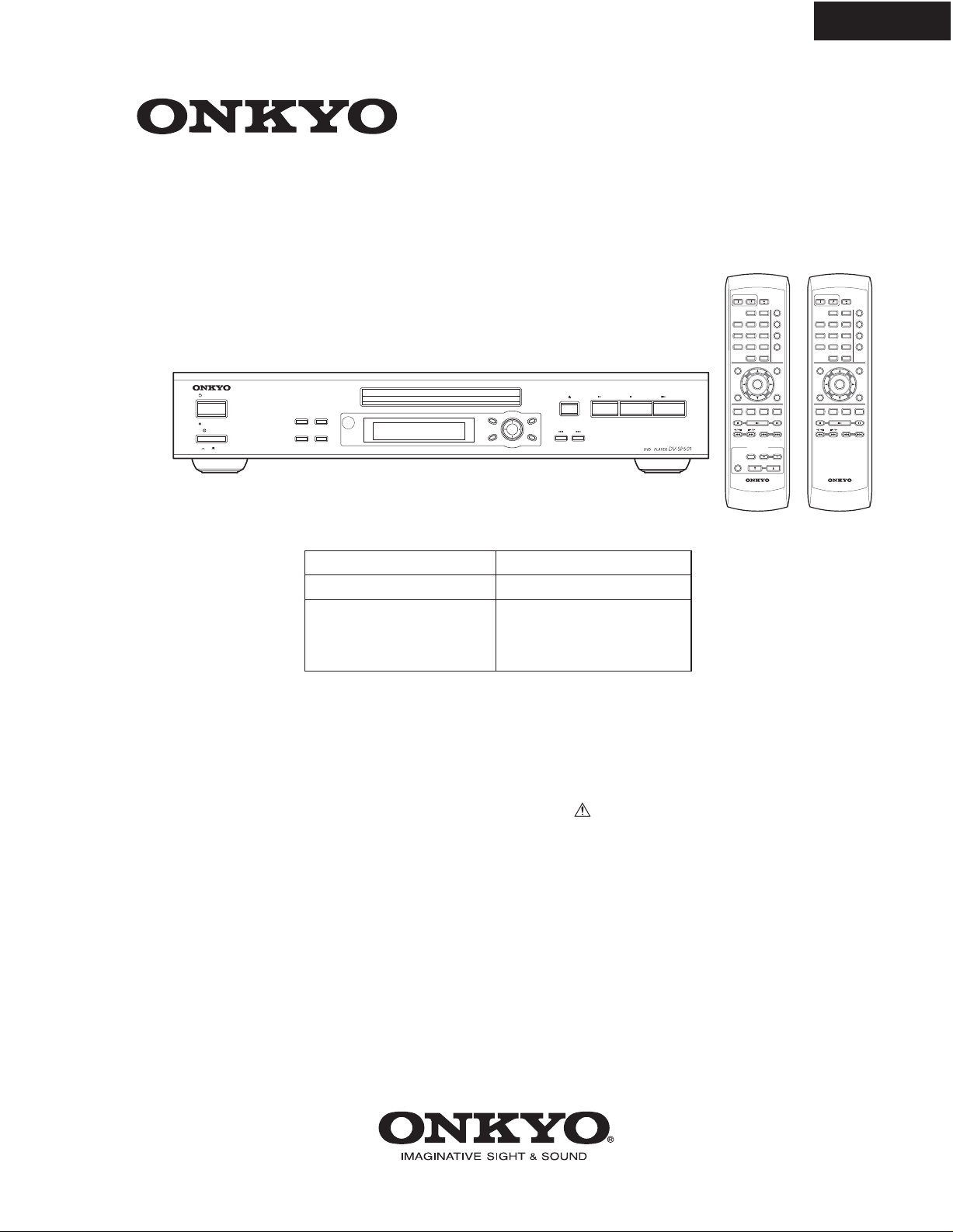
DVD PLAYER
DV-SP501
Ref. No. 3766
072003
STANDBY/ON
STANDBY
POWER
ON
ON STANDBY
OPEN/
MODEL DV-SP501
STOP
PAUSE
DISPLAY PLAY MODE
CLEAR
DIMMER
OFF
TOP MENU MENU
S
O
R
R
U
C
RETURN SETUP
P
U
R
S
E
H
T
N
T
E
O
Black, Silver and Golden models
BMDD1N, BMDC1N
BMUP2P, SMUP2P
120V AC, 60Hz
230-240V AC, 50Hz
PLAY
North American model
REPEAT
123
45
789
TOP MENU
RETURN
AUDIO
ANGLE SUBTITLE ZOOM
TV CONTROL
TV/VIDEO CHANNEL
ON/
STANDBY
RC-524DV
0
RC-524DV
CLOSE
RANDOM
-
A
B
PLAY MODE
DISPLAY
6
DIMMER
CLEAR
ENTER
VOLUME
ON STANDBY
OPEN/
CLOSE
RANDOM
-
A
B
REPEAT
PLAY MODE
123
DISPLAY
6
45
DIMMER
789
CLEAR
MENU
SETUP
0
TOP MENU
ENTER
RETURN
AUDIO ANGLE SUBTITLE ZOOM
RC-523DV
RC-523DV
Other models
MENU
SETUP
BMUS4P, BMUT3P,
GMUK3P, GMUR6P,
110-240V AC, 50/60Hz
GMUT3P, SMUS4P
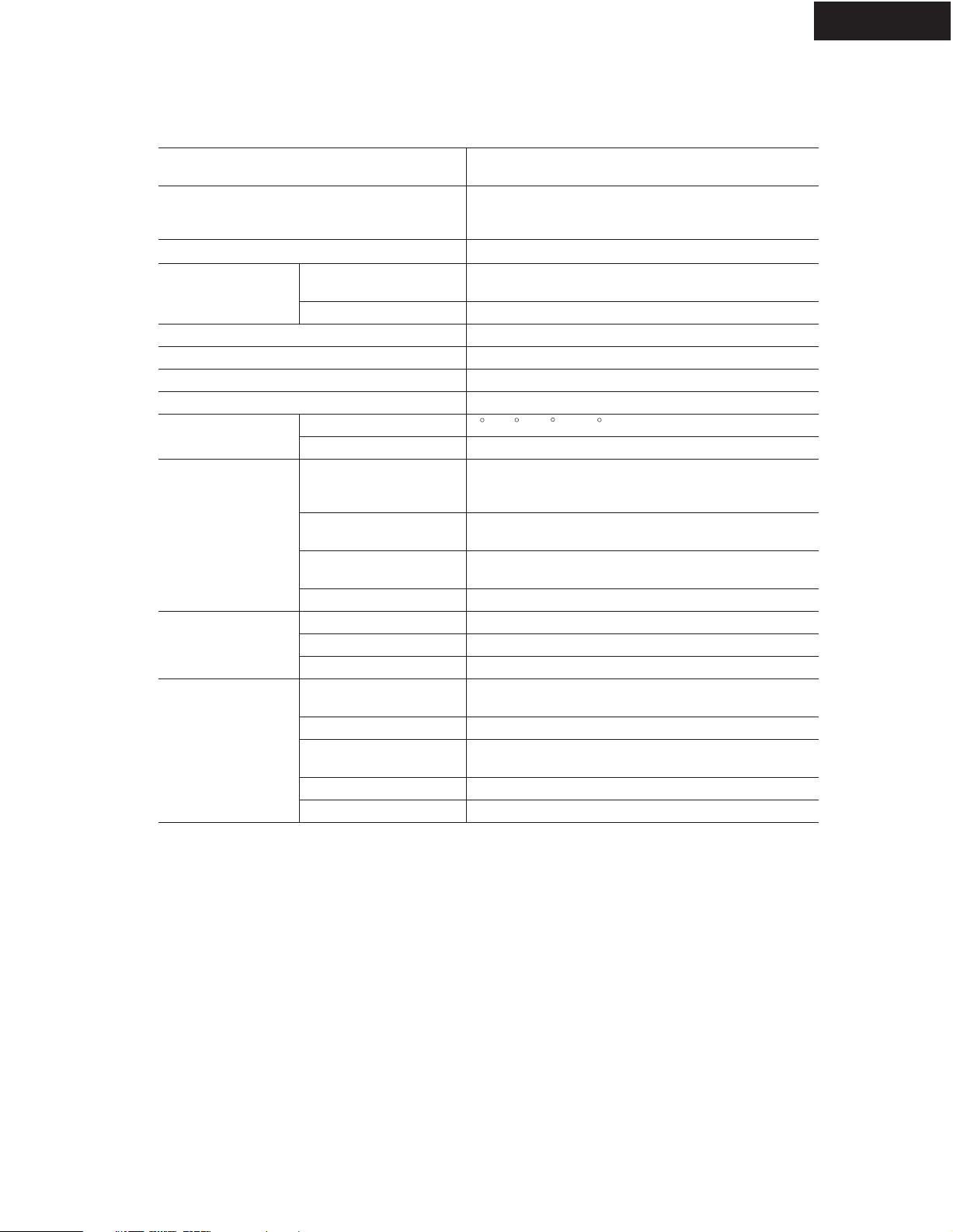
SAFETY-RELATED COMPONENT
WARNING!!
COMPONENTS IDENTIFIED BY MARK ON THE
SCHEMATIC DIAGRAM AND IN THE PARTS LIST ARE
CRITICAL FOR RISK OF FIRE AND ELECTRIC SHOCK.
REPLACE THESE COMPONENTS WITH ONKYO
PARTS WHOSE PART NUMBERS APPEAR AS SHOWN
IN THIS MANUAL.
MAKE LEAKAGE-CURRENT OR RESISTANCE
MEASUREMENTS TO DETERMINE THAT EXPOSED
PARTS ARE ACCEPTABLY INSULATED FROM THE
SUPPLY CIRCUIT BEFORE RETURNING THE
APPLIANCE TO THE CUSTOMER.
Page 2
SPECIFICATIONS
DV-SP501
Video system
Region code
Laser
Frequency response
Signal-to-noise ratio (digital audio) 106 dB
Audio dynamic range (digital audio) 96 dB
Harmonic distortion (digital audio) 0.008%
Wow and Futter Below measurable level (±0.001% (W. PEAK) or less)
Operating conditions
Video outputs
Audio outputs
General
DVD linear audio
CD audio 4 HzÐ20 kHz
Temperature 5 to 35 C (41 F to 95 F)
Installation Install horizontally
COMPONENT VIDEO
(Other than European
models)
AV CONNECTOR (European model only)
S VIDEO (S-Video)
VIDEO (composite video) 1.0 V (p-p), 75 ohm , negative sync, RCA/phono x1
OPTICAL -22.5 dBm, optical connector x1
COAXIAL 0.5 V (p-p), 75 ohm , RCA/phono x1
ANALOG 2.0 V rms, 470 , RCA/phono x1
Power supply
Power consumption 15 W
Power consumption in
Standby mode
Weight 3.3 kg (7.3 lbs.)
Dimensions (W x H x D) 435 X 81 X 307 mm (17-1/8" X 3-3/16" X 12-1/16")
North American model: Standard NTSC
Other models: PAL/AUTO
North American model: 1, European model: 2,
Australian and South American models: 4,
Asian model: 3, Chinese model: 6
Semiconductor laser, wavelength 650 nm (DVD), 780 nm (CD)
4 HzÐ20 kHz @ 48 kHz sampling rate
4 HzÐ44 kHz @ 96 kHz sampling rate
Y: 1.0 V (p-p), 75 ohm, negative sync, RCA/phono x1
B/PR: 0.7 V (p-p), 75 ohm
P
0.7 V (p-p), 75 ohm , Scart x1
Y: 1.0 V (p-p), 75 ohm , negative sync, 4-pin mini DIN x1
C: 0.286 V (p-p), 75 ohm
North American model: 120 V AC, 60 Hz
Other models: 100 - 240 V AC, 50/60 Hz
North American model: 1.6 W
Other models: 2.5 W
Specifications and features subject to change without notice.
Page 3
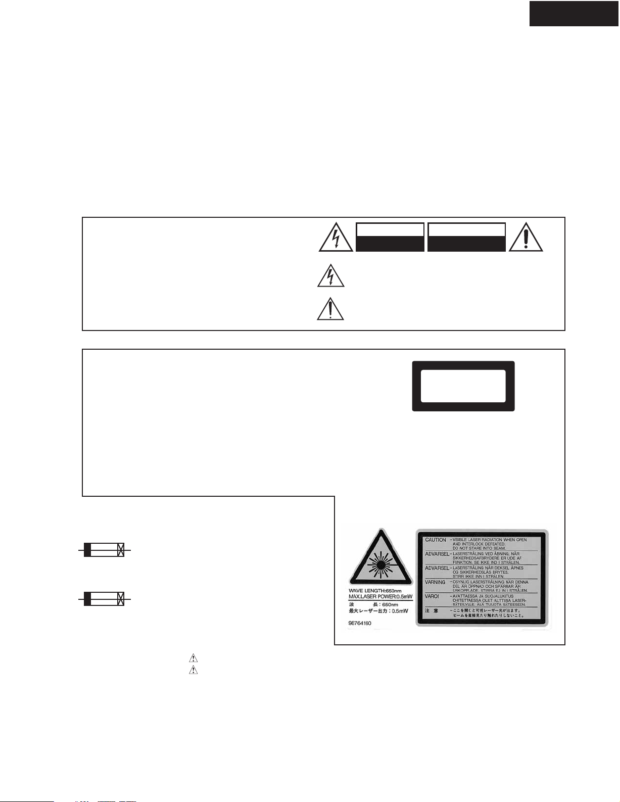
SERVICE PROCEDURES-1
PROTECTION OF EYES FROM LASER BEAM DURING SERVICING
This set employs a laser. Therefore, be sure to follow
carefully the instructions below when servicing.
WARNING!!
SERVICE WARNING : DO NOT APPROACH THE
LASER EXIT WITH THE EYE TOO CLOSELY.
IN CASE IT IS NECESSARY TO CONFIRM LASER
BEAM EMISSION, BE SURE TO OBSERVE FROM
A DISTANCE OF MORE THAN 30cm FROM THE
SURFACE OF THE OBJECTIVE LENS ON THE
OPTICAL PICKUP BLOCK.
WARNING
Laser Diode Properties
Wavelength: 650/780nm (DVD/CD)
DV-SP501
WARNING:
TO REDUCE THE RISK OF FIRE OR ELECTRIC SHOCK,
DO NOT EXPOSE THIS APPLIANCE TO RAIN OR
MOISTURE.
CAUTION:
TO REDUCE THE RISK OF ELECTRIC SHOCK, DO NOT
REMOVE COVER (OR BACK). NO USER-SERVICEABLE
PARTS INSIDE. REFER SERVICING TO QUALIFIED
SERVICE PERSONNEL.
LASER WARNING
This unit contains a semiconductor laser system and is classified
as a "CLASS 1 LASER PRODUCT". So, to use this model
properly, read this Instruction Manual carefully. In case of any
trouble, please contact the store where you purchased the unit.
To prevent being exposed to the laser beam, do not try to open
the enclosure.
CAUTION:
VISIBLE LASER RADIATION WHEN OPEN AND INTERLOCK
FAILED OR DEFEATED. DO NOT STARE INTO BEAM.
CAUTION:
THIS PRODUCT UTILIZES A LASER. USE OF CONTROLS OR
ADJUSTMENTS OR PERFORMANCE OF PROCEDURES
OTHER THAN THOSE SPECIFIED HEREIN MA
HAZARDOUS RADIATION EXPOSURE.
Y RESULT IN
SERVICE PROCEDURE
1. Replacing the fuses
WARNING
RISK OF ELECTRIC SHOCK
DO NOT OPEN
The lightning flash with arrowhead symbol, within an equilateral
triangle, is intended to alert the user to the presence of uninsulated
"dangerous voltage" within the product's enclosure that may be of
sufficient magnitude to constitute a risk of electric shock to persons.
The exclamation point within an equilateral triangle is intended to alert
the user to the presence of important operating and maintenance
(servicing) instructions in the literature accompanying the appliance.
The label on the right
is applied on the rear
panel except for USA
and Canadian
models.
1. This unit is a CLASS 1 LASER PRODUCT and employs a
laser inside the cabinet.
2. To prevent the laser from being exposed, do not remove
the cover. Refer servicing to qualified personnel.
LASER BEAM CAUTION LABEL
AVIS
RISQUE DE CHOC ELECTRIQUE
NE PAS
OUVRIR
"CLASS 1 LASER
PRODUCT"
This symbol located near the fuse indicates that the
fuse used is show operating type, For continued protection against
fire hazard, replace with same type fuse , For fuse rating, refer to
the marking adjest to the symbol.
Ce symbole indique que le fusible utilise est e lent.
Pour une protection permanente, n'utiliser que des fusibles de meme
type. Ce demier est indique la qu le present symbol est apposre.
REF. NO.
F1
PART NO.
252252 or 1.6A-TL/T-ST2 <MDD>,<MDC>
DESCRIPTION
252147 1.6A-TSC
252273 or 1.6A-SE-TL250V Except <MDD,MDC> modelF1
<MDD> : North American model
<MDC> : Canadian model
Page 4
SERVICE PROCEDURES-2
2. Safety-check out
(Only U.S.A. model)
After correcting the original service problem perform the
following safety check before releasing the set to the customer
Connect the insulating-resistance tester between the plug of
power supply cord and terminal GND on the back panel.
Specifications: More than 10M ohm at 500V
INITIALIZING
Factory-shipped condition.
Connect the power cord to inlet terminal.
Push button "ON" (Mechanical SW). Lighting the LED condition.
Press the [STOP] and [STANDBY] same time with NO DISC condition.
Push button "STANDBY".
Pull out the power cord.
DV-SP501
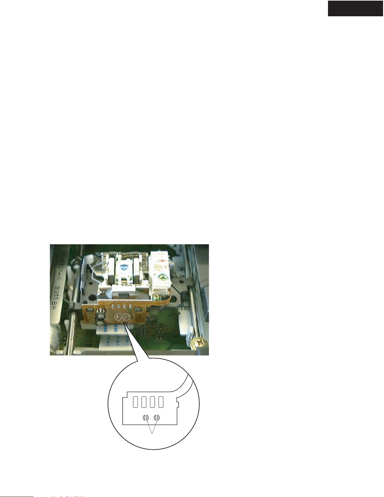
REMOVE THE SOLDER OF LASER DIODE SHORT
When replace the mechanism or DVD main PC board.
Shorting the solder of Shot-circuit land. (2 positions)
Mechanism
Short Land
Page 5
DV-SP501
03
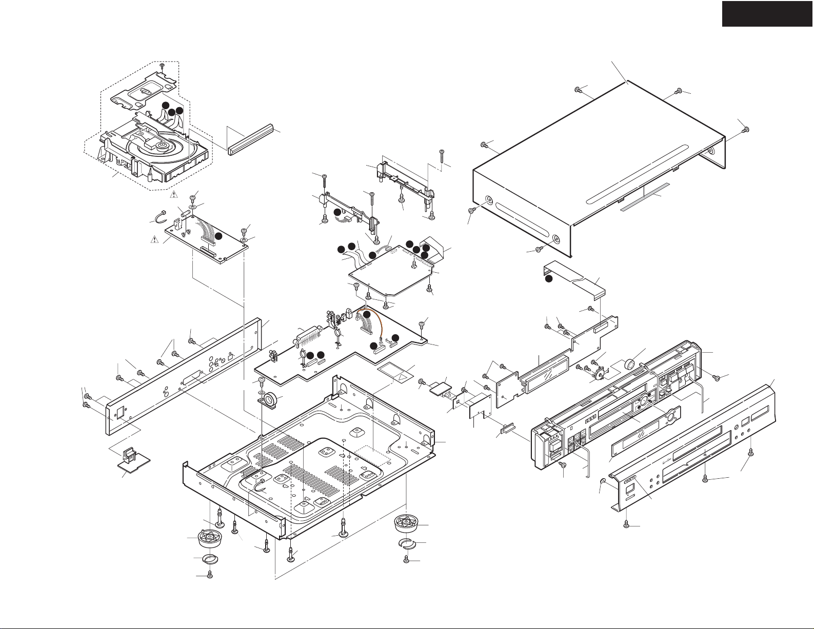
EXPLODED VIEW
a
Z10
P910
U20
A48
A48
A48
b
F1
A55
A56
A56
c
A51
H
T
L PA
A
IT
IG
D
T
A48
A11
A11a
f
Z91A
C
E
IR
D
A11
A11a
A47
M
Z14
Z12
PP only
A16
P901A
Z15
i
P503
A11
h
g
P502
i
A16
Z13
Z14
Z15
h
Z14
Z15
P702
a
d
g
b
c
A56
P501
Z1
A11
f
e
d
A11
A11
U1
A15
U4
A11
A32
A11
A56
A56
U2
e
A11
A11
S731
P701
A27 x 3
A35
A57
03
A19
A23
A56
A11
A41
U5
A3
A11
A13
A5
A10
P910
A12
A13
A3
A5
A11
U6
A1
U3
A30
A11
A23
A22
A44
A43
A46
A46
1
0
5
P
S
-
V
D
R
E
Y
A
L
P
D
V
D
Page 6
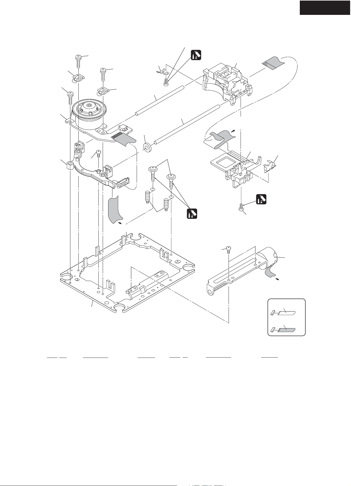
EXPLODED VIEW
DV-SP501
TRAVERSE MECHANISM
17
17
10
13
10
17
1
16
12
8
7
4 (Adjustment screw)
15 (Torque : 0.15 +/- 0.01 N•m)
Silicone Adhesive
GEM1037
6
3
To
DVDM CN101
(Pickup Assy)
14
9
Silicone Adhesive
GEM1037
(Adjustment
spring)
11
To DVDM CN102
(Spindle Motor)
TRAVERSE MECHA ASSY parts List
Mark No. Description Part No.
1 Spindle Motor VXM1099
2 Stepping Motor VXM1101
3 Pickup Assy-S OXX8005
4 Skew Screw VBA1080
5 Skew Spring VBH1335
6 Guide Bar VLL1514
7 Sub Guide Bar VLL1515
8 Leaf Spring VNC1023
5
Screw Tight
GYL1001
15 (Torque : 0.15 +/- 0.01 N•m)
16
Mark No. Description Part No.
9 Joint Spring VNC1019
10
NSP
Support Spring VNC1020
11 Mecha.Chassis VNE2248
12 Damper Sheet VEB1335
13 Spacer VNL1913
14 Joint 03 VNL1949
15 Tapping Screw OBA8016
16 Screw BBZ20P050FZK
17 Screw PMA26P100FMC
2
To
DVDM CN104
(Stepping Motor)
NON-CONTACT
SIDE
CONTACT SIDE
Page 7
EXPLODED VIEW / PARTS LIST
LOADING MECHANISM
DV-SP501
Note :
Refer to
" Application of Lubricant".
Daifree
GEM1036
23
Lubricating Oil
GYA1001
13
22
12
8
Refer to
2
"2.5 TRAVERSE MECHA. ASSY-S".
6
8
8
To DVDM CN101 (Pickup Assy-S)
To DVDM CN104 (Stepping Motor)
To DVDM CN102 (Spindle Motor)
8
20
18
22
16
17
3
A
4
5
19
15
14
22
LOADING MECHA ASSY parts List
Mark No. Description Part No.
NSP 1 LOAB Assy
2 Traverse Mecha. Assy-S VXX2871
3 Loading Motor Assy VXX2872
4 Motor Pulley
5 Motor
6 Flexible Cable (24P) VDA1945
7 Connector Assy 2P VKP2253
8 Floating Rubber VEB1351
9 Belt VEB1330
10 Stabilizer VNE2253
11 Loading Base VNL1917
12 Float Base DVD VNL1918
13 Drive Cam VNL1919
14 Gear Pulley VNL1921
15 Loading Gear VNL1922
16 Drive Gear VNL1923
21
22
7
A
10
11
Lubricating Oil
GYA1001
9
1
No. Description Part No.
Mark
17 SW Lever VNL1925
18 Clamper Plate VNE2251
19 Bridge VNE2252
20 Clamper VNL1924
21 Screw JGZ17P028FMC
22 Screw 801530
23 Tray VNL1920
NSP: Not service parts
Page 8
DV-SP501
OPTICAL_OUT
C360
104Z
L354
BK1608LM182-T
C363
223Z
1
2
3
4
C364
223Z
R411
1.5K
102
102
R412
1.5K
Q351 JFJ3000
3
2
1
R413
22K
C407
22K
C408
P350
P352RI_OUT
22K
R415
5
6
NJM4580M-D
R417
R421
R414
22K
R422
22K
GND_VIDEO
NC
R611
56K
R609
470
C409
NJM4580M-D
Q403
-B
4
C412
R428
10K
R614
RGBSW
68
P292A
TC4053BF
Y11
Z13
Z4
Z05
EN6
VEE7
GND8
1K
R610
100
7
NJM4580M-D
6
5
Q601
2SC2712
Q604
C415
47/50
C413
47/50
R613
1
25
R617
3
HN1A01F-GR
150K
RR461
150K
470
C410
10K
R430
Q404
+B
8
Y Y
P/XI
ASPECT
C C
V
G/Y
B/CB
R/CR
2.2K
R603
1.8K
R601
C602
104Z
C601
-B
Q401
4
R416
VSEL2
R423
7
R419
22K
22K
5
-B
Q402
6
NJM4580M-D
22K
R418
1.5K
NJM4580M-D
1.5K
4
SQUEEZE
4.7K
R606
1
1.5K
7
R420
100/16
8
Q403
R424
1.5K
2.2K
R602
10K
10K
R605
R604
Q602
Q603
DTC114EE
DTC114EE
SW+5V SW+5V
1.2K
22K
R608
R607
Q606
2SA1162
Q605 2SC2712
R429 10K
3
+B
R427
2
10K
6
5
C411 220/6.3
3
4
220/6.3
-B
1
Q404
2
NJM4580M-D
VCC16
X113
X012
10K
V+12V
330 1/2W
R/C.DRV
Q607
R431
470
R432
R443
270
R461
150K
47/50
Y1 5Y02
X1 4
A1 1
B1 0
C9
R615
C419
7
470
R458
P201
P201
G1
1
Y
3
G2
5
C
4
G3
2
7
8
4
2
1
3
S-Video out
G4
SIGNAL
P203
Y
CB
Video out
Except <MUP>
CR
P601
SCART
AUDIO_R1
2
AUDIO_L3
AGND4
VGND15
6
B7
F.SW8
VGND29
10
G11
12
VGND313
VGND414
R/C15
SCART TERMINAL
RGB.SW16
VGND517
VGND618
CV/Y19
20
VGND721
C221
NC
R224 10K
C222 104K
Except <MUP>
C2241000/6.3
C2251000/6.3
C2261000/6.3
B/CB
C603
6
4
Q405
100/16
R453
100
HN1C03F
5
R454
2.2K
C418
NC
3
4
1000/6.3
<MUP> : European model
D601 1SS226
NC
D602
1SS226
NC
D603 1SS226
NC
D604
1SS226
NC
D605 1SS226
NC
R441
D606 1SS226
3
Q407
4
R455
NC
C480
100K
R433
100K
100
C482
RGBSW
Y/V.DRV
NC
Y
V
R/C
Y/V
G/Y
0
R626
R612
330 1/2W
Y/V.DRV
6
1
100
25
R616
4
3
Q608
HN1A01F-GR
Q407
6
HN1C03F
2
1
R452
2.2K
R447 100
HN1C03F
6
HN1C03F
Q405
2
R445
2.2K
5
R449
2.2K
1
C416
470/6.3
C223
470/6.3
<MUP> only
C612
470/6.3
C613
470/6.3
R/C.DRV
C614
470/6.3
C615
470/6.3
R435
100
R221
R222
R223
R618
R619
R620
R621
R231
R229
R227
0
L201
R232
0
L202
R233
0
L203
0
L204
R225
R236
75
0
R622
L601
R623
L602
L604
R624
L603
R625
L205
R235
0
L206
0
0
0
0
75
75
75
75
75
75
75
75
75
NC
C414
47/50
MUTE_R
150K
R459
R446
2
Q406
HN1C03F
R444
270
2.2K
1
6
C417
NC
R450
2.2K
HN1C03F
R448
100
Q406
5
4
R442
100K
NC
3
C481
R434
100
R ch
3
1
L ch
2
4
P401
MONO
Audio out
Page 9
A
BCDEFGH
SCHEMATIC DIAGRAM
Not use
1
To Display circuit PC board NADIS-7998
P701A
1
VSEL1
2
2
3
4
5
VSEL2
3
SQUEEZE
4
LETTER
5
ASPECT
6
P/XI
7
RGB
8
CY/G
9
GND1
10
CB/B
11
GND2
12
CR/R
13
DNG3
From DVD Main circuit PC board
C
14
15
GND4
16
V
17
GND5
Y
18
CN903
1
GND4
2
Y1
3
GND3
4
V
5
GND2
6
C
7
GND1
8
DVDA2
9
DVDL
10
GNDA1
From DVD Main circuit PC board
11
DVDR
CN902
1
CTS
2
RTS
3
RXD
4
TXD
5
XVMUTE
6
DVDMUTE
7
DVDTRKUP
8
VDET
9
GNDD6
10
GNDD5
11
ARK
12
MDATA
13
SDATA
14
SCLK
15
SYS_CS2
16
SYS_CS1
17
XDVDRST
18
DVDPOWER
19
GNDD4
20
GNDD3
21
DOUT
From DVD Main circuit PC board
22
GNDD2
23
GNDD
24
GNDM2
25
GNDM
26
VPR+8M1
27
VPR+8M2
28
VPR+8A1
29
VPR+8A2
30
VDVD+12
CN901
P104
1
TXD
2
RXD
3
DTR
4
CTS
5
V+5D
For Download
1mm Pich FFC
6
GNDD
7
NC
U1 : OUTPUT TERMINAL PC BOARD
-27V
RI
FLAC1
VDET
FLAC2
IRIN
EVER+5V
ACK
GND
DEMO
SYSRESET
RESET
P_ON
XSCK
XRDY
SI
SO
R102 47
VSEL1
R103 47
VSEL2
R104 47
SQUEEZE
R106 47
ASPECT
R107 47
P/XI
R108 47
RGB
G/Y
B/CB
R/CR
CS I
V XSCK
Y
R121 47
R122 47
R125 47
R127 47
CTS VSEL1
DTR
RXD
TXD
R123 0
VDET
ACK
R124 47
SI
R126 47
SO
XSCK
XRDY
SYSRESET
P_ON
DOUT
C909
104Z
C910
1000/16
R135 10K
R134 10K
R137 10K
R136 10K
TXD
RXD
DTR
CTS
R118
DEMO
10K
NAAR-7997
R101 10K
P702B
MUP2P
OTHER
RESET
220/16
C101
104Z
R119
10K
UDZ5B
D101
RGB
P351A
DOUT
GND
SO
NC
MRESET
RGB
R115
0
0
R116
C903
104Z
C907
104Z
1000/16
C914
104Z
C911
100/16
-27V
GND
FLAC1
15 10 5 1
V+12V
FLAC2
From Power supply unit
C902
IC
P105
R115R116
0
--0
10K
R117
C901
104Z
C908
P901
L351 BK1608LM182-T
DVDMUTE
C904
220/6.3
+8V
GND
M+8V
R351
MGND
0
SW+5V
GND
C352 104Z
C905 104Z
R462
1K
P_ON
EVER+5V
C353 100/6.3
C906 220/16
D460
D923
D924
1K
NC
R352
R920
D920
R463
R353 470K
1SS352
1SS352
D921
1SS352
1SS352
+12V
220
C920
UDZS11B
C420
2SC2712
470/6.3
NC
Q352
TC74VHCU04T
Q920
10/16
D922
1SS352
OPTICAL_OUT
C354
C356
020
C357
104K
8
9
101112
13
VCC 14
12345
GND
V+12V V+12V
R902
2.2K
D901
UDZS5.1B
R482
2.2
(1/4W)
220/16
C401
47/16
V+6V
100K
AGND
100K
C402 47/16
Q460
DTA114YKA
Q463
DTC144YKA
GND7
6
BK1608LM182-T
R357 470
+6V
C923 104Z
C922 220/16
C485
1.5K
R401
R457
V+6V
R456
R402
1.5K
330
R354
180
L352
C921
C486
220/16
681
C403
R403
NC
681
C404
180
220
R355
R356
C361
104Z
L353 BK1608LM182-T
SW+5V
V+11V
220/16
2.2
R481
(1/4W)
3
0
R405
2
NC
10K
R407
152
C405
152
C406
R404
0
R406
10K
R408
3
2
C358
C362
220
Q401
C359
100/6.3
NJM4580M-D
8
+B
R409
10K
8
+B
Q402
R410
10K
BK1608LM182-T
AGND
1
NJM4580M-D
1
R411
C363
223Z
C364
223Z
R412
1.5K
L354
1.5K
Page 10
DV-SP501
A
SCHEMATIC DIAGRAM
Not use
1
To Display circuit PC board NADIS-7998
P701A
1
VSEL1
2
2
3
4
5
VSEL2
3
SQUEEZE
4
LETTER
5
ASPECT
6
P/XI
7
RGB
8
CY/G
9
GND1
10
CB/B
11
GND2
12
CR/R
13
DNG3
From DVD Main circuit PC board
C
14
15
GND4
16
V
17
GND5
Y
18
CN903
1
GND4
2
Y1
3
GND3
4
V
5
GND2
6
C
7
GND1
8
DVDA2
9
DVDL
10
GNDA1
From DVD Main circuit PC board
11
DVDR
CN902
1
CTS
2
RTS
3
RXD
4
TXD
5
XVMUTE
6
DVDMUTE
7
DVDTRKUP
8
VDET
9
GNDD6
10
GNDD5
11
ARK
12
MDATA
13
SDATA
14
SCLK
15
SYS_CS2
16
SYS_CS1
17
XDVDRST
18
DVDPOWER
19
GNDD4
20
GNDD3
21
DOUT
From DVD Main circuit PC board
22
GNDD2
23
GNDD
24
GNDM2
25
GNDM
26
VPR+8M1
27
VPR+8M2
28
VPR+8A1
29
VPR+8A2
30
VDVD+12
CN901
P104
1
TXD
2
RXD
3
DTR
4
CTS
5
V+5D
For Download
1mm Pich FFC
6
GNDD
7
NC
U1 : OUTPUT TERMINAL PC BOARD
-27V
RI
FLAC1
VDET
FLAC2
IRIN
EVER+5V
ACK
GND
DEMO
SYSRESET
RESET
P_ON
XSCK
XRDY
SI
SO
R102 47
VSEL1
R103 47
VSEL2
R104 47
SQUEEZE
R106 47
ASPECT
R107 47
P/XI
R108 47
RGB
G/Y
B/CB
R/CR
CS I
V XSCK
Y
R121 47
R122 47
R125 47
R127 47
CTS VSEL1
DTR
RXD
TXD
R123 0
VDET
ACK
R124 47
SI
R126 47
SO
XSCK
XRDY
SYSRESET
P_ON
DOUT
C909
104Z
C910
1000/16
R135 10K
R134 10K
R137 10K
R136 10K
TXD
RXD
DTR
CTS
R118
DEMO
10K
BCDEFGH
NAAR-7997
1
3
5
4
2
7
8
P201
P201
G1
Y
G2
C
G3
S-Video out
G4
SIGNAL
P203
4
Y
2
CB
1
3
3
1
2
4
Video out
Except <MUP>
CR
P601
SCART
AUDIO_R1
2
AUDIO_L3
AGND4
VGND15
6
B7
F.SW8
VGND29
10
G11
12
VGND313
VGND414
R/C15
SCART TERMINAL
RGB.SW16
VGND517
VGND618
CV/Y19
20
VGND721
R ch
L ch
Audio out
MONO
P401
C101
104Z
D101
R119
R101 10K
UDZ5B
C360
104Z
1
2
3
4
102
102
Q351 JFJ3000
3
2
1
R413
22K
C407
22K
C408
P350
P352RI_OUT
22K
R415
5
6
NJM4580M-D
R417
R421
R414
22K
R422
22K
GND_VIDEO
NC
R611
56K
R609
470
C409
NJM4580M-D
Q403
-B
4
C412
R428
10K
R614
RGBSW
68
P292A
TC4053BF
Y11
Z13
Z4
Z05
EN6
VEE7
GND8
1K
R610
100
7
NJM4580M-D
6
5
Q601
2SC2712
Q604
C415
47/50
C413
47/50
R613
1
25
R617
3
HN1A01F-GR
150K
RR461
150K
470
C410
10K
R430
Q404
+B
8
Y Y
P/XI
ASPECT
C C
V
G/Y
B/CB
R/CR
2.2K
R603
1.8K
R601
C602
104Z
C601
100/16
2.2K
R602
10K
10K
R605
R604
SQUEEZE
4.7K
R606
1
NJM4580M-D
1.5K
R424
7
R420
1.5K
Q602
Q603
DTC114EE
DTC114EE
SW+5V SW+5V
1.2K
22K
R608
R607
Q606
2SA1162
Q605 2SC2712
R429 10K
3
8
+B
R427
Q403
2
10K
6
5
C411 220/6.3
3
4
220/6.3
-B
1
Q404
2
NJM4580M-D
-B
Q401
4
R416
VSEL2
R423
7
R419
22K
22K
5
-B
Q402
6
NJM4580M-D
22K
R418
1.5K
1.5K
4
VCC16
10K
V+12V
330 1/2W
R/C.DRV
Q607
R431
470
R443
270
R461
150K
47/50
X113
X012
R432
Y1 5Y02
X1 4
A1 1
B1 0
C9
R615
C419
7
470
R458
Y
V
0
R626
6
4
C414
47/50
MUTE_R
OPTICAL_OUT
C354
+12V
220
C920
UDZS11B
C420
2SC2712
470/6.3
NC
Q352
TC74VHCU04T
Q920
10/16
D922
1SS352
C356
020
C357
104K
8
9
101112
13
VCC 14
12345
GND
V+12V V+12V
R902
2.2K
D901
UDZS5.1B
R482
2.2
(1/4W)
220/16
C401
47/16
V+6V
100K
AGND
100K
C402 47/16
Q460
DTA114YKA
Q463
DTC144YKA
GND7
6
BK1608LM182-T
R357 470
+6V
C923 104Z
C922 220/16
C485
1.5K
R401
R457
V+6V
R456
R402
1.5K
330
R354
180
L352
C921
C486
220/16
681
C403
R403
NC
681
C404
180
220
R355
R356
C361
104Z
L353 BK1608LM182-T
SW+5V
V+11V
220/16
2.2
R481
(1/4W)
3
0
R405
2
NC
10K
R407
152
C405
152
C406
R404
0
R406
10K
R408
3
2
C358
C362
220
Q401
C359
100/6.3
NJM4580M-D
8
+B
R409
10K
8
+B
Q402
R410
10K
BK1608LM182-T
AGND
1
NJM4580M-D
1
R411
C363
223Z
C364
223Z
R412
1.5K
L354
1.5K
L351 BK1608LM182-T
P351A
NC
GND
C352 104Z
C905 104Z
R462
1K
P_ON
EVER+5V
C353 100/6.3
C906 220/16
D460
D923
D924
1K
R352
R920
D920
R463
R353 470K
1SS352
1SS352
D921
1SS352
1SS352
DOUT
R351
0
GND
SO
NC
MRESET
IC
P105
P702B
RGB
0
MUP2P
--0
OTHER
10K
R117
RESET
C902
C901
220/16
C908
P901
10K
RGB
R115
0
R115R116
0
R116
DVDMUTE
C904
C903
104Z
220/6.3
104Z
C907
104Z
1000/16
C914
104Z
C911
100/16
+8V
GND
-27V
GND
M+8V
FLAC1
15 10 5 1
V+12V
FLAC2
From Power supply unit
MGND
SW+5V
1
100
25
R616
3
HN1C03F
HN1C03F
Q405
2
R/C
Y/V
R612
330 1/2W
Y/V.DRV
Q608
HN1A01F-GR
Q407
2
R452
2.2K
R447 100
6
1
R445
2.2K
150K
NC
G/Y
6
1
HN1C03F
R449
R459
HN1C03F
Q405
5
2.2K
C416
Q406
R444
270
B/CB
C603
6
4
NC
R446
R453
R454
2.2K
2
100/16
100
HN1C03F
5
2.2K
C418
NC
3
4
1
6
R224 10K
C222 104K
Except <MUP>
C2241000/6.3
C2251000/6.3
C2261000/6.3
1000/6.3
<MUP> : European model
D601 1SS226
NC
D602
1SS226
NC
D603 1SS226
NC
D604
1SS226
NC
D605 1SS226
NC
D606 1SS226
3
Q407
NC
4
C482
R455
100K
100
R433
NC
C480
R441
100K
C417
NC
Q406
4
R450
HN1C03F
R448
R442
2.2K
5
3
100
Y/V.DRV
100K
NC
C481
RGBSW
C221
470/6.3
C223
470/6.3
<MUP> only
C612
470/6.3
C613
470/6.3
R/C.DRV
C614
470/6.3
C615
470/6.3
R435
100
100
R434
R221
R222
R223
R618
R619
R620
R621
R231
R229
R227
0
L201
R232
0
L202
R233
0
L203
0
L204
R225
R236
75
0
R622
L601
R623
L602
L604
R624
L603
R625
L205
R235
0
L206
0
0
0
0
75
75
75
75
75
75
75
75
75
Page 11
DV-SP501
MJJ MDD MUP MUT/MUK MUS/MUA
Region 643212
0
0
R738
R739
R740
R741
R742
R743
R739R738
R740 R741
R742 R743
INIT1
INIT2
R708 0 NC
R709 NC 0
SYSIN
VDET
SYSOUT
REMO
IRIN
NC
ACK
DEMO -27V
SYSRESET
Q705
REMSENS
R727
REMO
Integra Others
47K
R712
D703
1SS352
Q704
RN2403
K1 K1
R751
2.7K
0
C706
100/6.3
R713
220K
D702
UDZS5.6B
STB_L STB_L
K0 K0
R758
2.7K
2.7K
R766
NC
NC
0
0
NC
NC
NC
0
1KNCNC
NC
R752
390
CLEAR
T.MENU
K2
PAUSE
R753
470
R759
R767
1K
0
NC
0
390
390
S712
PLAY MODE
S704
RETURN
S701
STOP
GND
0
NC
1K
0
NC
R754
820
R760
R768
NC
470
470
S713
S705
S702
R755
DISPLAY
MENU
PLAY
1K
NC
NC
1K
NC
S714
R761
820
R769
820
0
0
S706
S703
R756
1.8K
SETUP
MUR
NC
1K
NC
1K
NC
1K
DIMMER
R762
1K
S707
R770
1K
S715
R763
1.8K
R771
1.8K
DOWN
U3 : STANDBY SWITCH
PC BOARD NADIS-7999
JL703B
R764
3.9K
R772
3.9K
JL703A
S708
R765
10K
UP
OPEN
S709
R773
10K
UP
RIGHT
DOWN
LEFT
S710
P731
R757
3.9K
STANDBY
7
6
5
4
3
2
1
S716
Q708
RN1407
ENTER
S731
NPS-115-S673
R779
D721
470
STANDBY
10K
R701
1M
R711
X701
5.00MHZ
P982A
R710 10K
104Z
P702A
C703
D701
Q703
S-80145
3
4
2
5
1
U5 : INLET TERMINAL
PC BOARD NAPS-8001
P981A
P982BP982A
AC INLET
P981
FLAC1
FLAC2
XRDY
SO
XSCK
PON
SI
RESET
20 10
SYSRESET
GND
DEMO
GND
P701A
ACK
E+5V
IRIN
To Out put terminal PC board NAAR-7997
CAUTION
FOR CONTINUED PROTECTION
AGAINST FIRE HAZARD, REPLACE
ONLY WITH FUSE OF SAME TYPE
VA
AND RATING INDICATED.
ATTENTION
AFIN D'ASSURER UNE PROTECTION
PERMANENTE CONTRE LES RISQUES
D'INCENDIE, REMPLACER UNIQUEMENT
VA
PAR UN FUSIBLE DE MEME TYPE
ET CALIBRATION COMME INDIQUE.
THIS SYMBOL LOCATED NEAR THE FUSE INDICATES
THAT THE FUSE USED IS SLOW OPERATING TYPE
FOR CONTINUED PROTECTION AGAINST FIRE
HAZARD,REPLACE WITH SAME TYPE FUSE. FOR FUSE
RATING REFER TO THE MARKING ADJACENT TO THE SYMBOL.
CE SYMBOLE INDIQUE QUE LE FUSIBLE UTLISE EST
E LENT.POUR UNE PROTECTION PERMANENTE,N'UTILISER
QUE DES FUSIBLES DE MEME TYPE. CE DARNIER EST
INDIQUE LA QU LE PRESENT SYMBOL EST APPOSE.
FLAC1
VDET
FLAC2RI-27V
232BU
SRESET
232RE
232SO
232SI
232SCK
1
Page 12
A
SCHEMATIC DIAGRAM
1
B C DE FG H
U2 : DISPLAY CIRCUIT PC BOARD NADIS-7998
Model Setup
Integra Others
R736 NC 0
R737 1K NC
Q702HNV-13SS12T
P218
P317
P416
P515
10K
R720
41
42
P614
SRESET
10K
R719
STBYLED
R232RES 40
NC543
NC644
42: NC4
NC745
NC846
NC947
NC1048
NC1149
P1550
P1451
P1352
P1253
P1154
P1055
P956
P857
P758
VDD259
VLOAD60
P661
P6P5P4P3P2
P713
P812
MSO_0
MSO_1
39
MSO_0 38
MSO_1 37
FLON_OFF
P364
P463
P562
P911
MSO_2
MSO_2 36
P265
P1010
P10
INIT0
P1
P119
P128
P137
P11
P12
P13
INIT1
INIT2
232SO
R7180
INIT0 35
INIT1 34
INIT2 33
MPD780232GC
OPEN67
P166
13G68
13G
12G
F122
P146
P155
P14
P15
232SCK
232SI
232BU
232RE
SYSOUT
R7170
100
100
R714
R715 100
R716
232SO 32
R232SI 30
232SCK 31
SYSOUT 27
R232REQ 28
R232BUSY 29
Q701
10G71
11G70
12G69
11G
7G74
8G73
9G72
9G8G7G6G5G4G3G2G1G
10G
F11
1G41
2G40
3G39
4G38
5G37
6G36
7G35
8G34
F245
F2244
1G2G3G4G5G6G7G8G9G
2
NC
0
Q707
R726
9G33
10G32
11G31
12G30
13G29
10G
11G
12G
13G
NC
Q706
R725
0
2S
R724
0
FL_ON/OFF ENTER
10K
R723
STB_L K2 RI
P119
P1P2P3P4P5P6P7P8P9
10K
10K
R721
R722
3
R
100KX5
P15 PON
P14 XRDY
P13 SO
P12 SI
P11 XSCK
P10
P9
P8
P7
4
C705
22/50
SYSIN
C704
104Z
+5V 24
VDD0 25
SYSIN 26
DISPKLAYMODE 13
4G77
5G76
6G75
NC
R737R736
0
MSO_0
K0
K1
K0 22
K1 21
VSS0 23
VDET 19
AVSS 18
VCOFF 17
REMO 16
SYSRESET 12
PON 11
XRDY 10
XSCK 7
RESET 6
VSS1 2
VDD1 1
1G80
2G79
3G78
K2 20
IRIN 15
ACK 14
SO 9
X2 4
X1 3
MSO_1
SI 8
IC 5
1K
R733
0
R734
MSO_2
C702
104Z
INIT0
0
R709
R708
R707 0
R706 0
R705 0
R704 0
R703 100
R702 0
C701
100/6.3
R742 R743
INIT1
VDET
REMO
IRIN
NC
ACK
DEMO -27V
SYSRESET
10K
R701
1M
R711
U20 : POWER SUPPLY UNIT
NGPS-0040 AC100-120V 50Hz/60Hz
NGPS-0041 AC100-240V 50Hz/60Hz
AC G
5
FLAC1
FLAC
-27V
NC
GND
EVRE+12V
GND
E+8V
M+8V
NC
GND
SW+5V
GND
EVER+5V
P ON
CN2
To Out put terminal PC board NAAR-7997 CN901
AC H
U4 : POWER SWITCH
CN1
PC BOARD NASW-8000
S991
P982B
C991
103M/250V
Page 13
DV-SP501
A
SCHEMATIC DIAGRAM
1
2
3
4
5
B C DE FG H
U2 : DISPLAY CIRCUIT PC BOARD NADIS-7998
Q702HNV-13SS12T
P218
P317
P416
P515
10K
R720
41
42
P614
SRESET
10K
R719
STBYLED
R232RES 40
NC543
NC644
42: NC4
NC745
NC846
NC947
NC1048
NC1149
P1550
P1451
P1352
P1253
P1154
P1055
P956
P857
P758
VDD259
VLOAD60
P661
P6P5P4P3P2
P713
P812
MSO_0
MSO_1
39
MSO_0 38
MSO_1 37
FLON_OFF
P364
P463
P562
P911
MSO_2
MSO_2 36
P265
P1010
P10
INIT0
P1
P119
P128
P11
P12
INIT1
INIT2
INIT0 35
INIT1 34
MPD780232GC
OPEN67
P166
13G
1G41
F245
F2244
1G2G3G4G5G6G7G8G9G
NC
Q707
2G40
3G39
4G38
5G37
6G36
7G35
8G34
9G33
10G32
11G31
12G30
13G29
10G
11G
12G
13G
NC
Q706
0
R725
0
R726
2S
R724
0
FL_ON/OFF ENTER
10K
R723
STB_L K2 RI
R
100KX5
P15 PON
P14 XRDY
P13 SO
P12 SI
P11 XSCK
P10
P9
P8
P7
P119
P1P2P3P4P5P6P7P8P9
10K
10K
R721
R722
C705
22/50
U20 : POWER SUPPLY UNIT
NGPS-0040 AC100-120V 50Hz/60Hz
NGPS-0041 AC100-240V 50Hz/60Hz
FLAC1
FLAC
-27V
NC
GND
EVRE+12V
GND
E+8V
M+8V
NC
GND
SW+5V
GND
EVER+5V
P ON
CN2
To Out put terminal PC board NAAR-7997 CN901
P137
P146
P155
P13
P14
P15
232SO
232SCK
232SI
232BU
R7170
R7180
100
R715 100
R716
INIT2 33
232SO 32
R232SI 30
232SCK 31
R232BUSY 29
Q701
10G71
11G70
12G69
13G68
9G72
9G8G7G6G5G4G3G2G1G
12G
11G
10G
Model Setup
Integra Others
R736 NC 0
R737 1K NC
F122
F11
MSO_0
232RE
SYSIN
SYSOUT
C704
104Z
100
R714
+5V 24
VDD0 25
SYSIN 26
SYSOUT 27
R232REQ 28
DISPKLAYMODE 13
4G77
5G76
6G75
7G74
8G73
CN1
AC G
AC H
MSO_1
SI 8
IC 5
1K
R733
0
R734
MSO_2
C702
104Z
INIT0
0
R709
R708
R707 0
R706 0
R705 0
R704 0
R703 100
R702 0
C701
100/6.3
R742 R743
INIT1
VDET
REMO
IRIN
NC
ACK
DEMO -27V
SYSRESET
10K
R701
1M
R711
NC
R737R736
0
K0
K1
K0 22
K1 21
VSS0 23
K2 20
VDET 19
AVSS 18
VCOFF 17
REMO 16
IRIN 15
ACK 14
SYSRESET 12
PON 11
XRDY 10
SO 9
XSCK 7
RESET 6
X2 4
X1 3
VSS1 2
VDD1 1
1G80
2G79
3G78
U4 : POWER SWITCH
PC BOARD NASW-8000
S991
P982B
C991
103M/250V
R739R738
R740 R741
INIT2
R708 0 NC
R709 NC 0
SYSIN
SYSOUT
X701
R710 10K
5.00MHZ
P982A
Q705
REMSENS
0
R727
C706
100/6.3
REMO
Integra Others
R713
220K
D702
UDZS5.6B
Q703
S-80145
3
4
2
5
1
Q704
RN2403
104Z
47K
R712
C703
P702A
D703
D701
1SS352
U5 : INLET TERMINAL
PC BOARD NAPS-8001
P981A
P982BP982A
AC INLET
Region 643212
R738
R739
R740
R741
R742
R743
K1 K1
R751
2.7K
STB_L STB_L
K0 K0
R758
2.7K
2.7K
R766
P981
MJJ MDD MUP MUT/MUK MUS/MUA
0
0
0
NC
0
NC
0
NC
K2
R752
390
NC
0
NC
NC
1KNCNC
R753
470
CLEAR
R759
T.MENU
R767
PAUSE
1K
0
NC
0
S712
390
390
FLAC1
FLAC2
S704
S701
GND
R754
PLAY MODE
RETURN
STOP
NC
1K
0
NC
820
R760
R768
0
NC
NC
NC
1K
0
NC
R755
1K
S713
S714
DISPLAY
R761
470
820
MENU
S706
S705
R769
470
820
PLAY
S702
S703
XRDY
SO
XSCK
PON
SI
20 10
To Out put terminal PC board NAAR-7997
MUR
NC
1K
NC
1K
NC
1K
R756
1.8K
S715
DIMMER
R763
R762
1.8K
1K
S707
SETUP
R770
1K
SYSRESET
RESET
VA
THIS SYMBOL LOCATED NEAR THE FUSE INDICATES
THAT THE FUSE USED IS SLOW OPERATING TYPE
FOR CONTINUED PROTECTION AGAINST FIRE
HAZARD,REPLACE WITH SAME TYPE FUSE. FOR FUSE
RATING REFER TO THE MARKING ADJACENT TO THE SYMBOL.
CE SYMBOLE INDIQUE QUE LE FUSIBLE UTLISE EST
E LENT.POUR UNE PROTECTION PERMANENTE,N'UTILISER
QUE DES FUSIBLES DE MEME TYPE. CE DARNIER EST
INDIQUE LA QU LE PRESENT SYMBOL EST APPOSE.
DOWN
R771
1.8K
GND
DEMO
GND
ACK
P701A
CAUTION
FOR CONTINUED PROTECTION
AGAINST FIRE HAZARD, REPLACE
ONLY WITH FUSE OF SAME TYPE
VA
AND RATING INDICATED.
ATTENTION
AFIN D'ASSURER UNE PROTECTION
PERMANENTE CONTRE LES RISQUES
D'INCENDIE, REMPLACER UNIQUEMENT
PAR UN FUSIBLE DE MEME TYPE
ET CALIBRATION COMME INDIQUE.
U3 : STANDBY SWITCH
PC BOARD NADIS-7999
JL703B
E+5V
R764
3.9K
R772
3.9K
IRIN
JL703A
S708
FLAC1
UP
VDET
R765
10K
OPEN
S709
R773
10K
FLAC2RI-27V
UP
RIGHT
DOWN
LEFT
232BU
S710
SRESET
P731
232RE
R757
3.9K
232SO
232SI
STANDBY
7
6
5
4
3
2
1
232SCK
1
S716
RN1407
ENTER
470
R779
D721
STANDBY
Q708
S731
NPS-115-S673
Page 14
DV-SP501
5V Reg.
(D) (D)
(Y)
(C/V)
(C)
(PR/R)
(PB/B)
(CY/G)
2/3
(D)
2/3
(C/V)
(PR/R)
(PB/B)
(CY/G)
(Y)
(C)
(D)
TO OUTPUT TERMINAL PC BOARD CN901
(Y)
(C/V)
(C)
(PR/R)
(PB/B)
(CY/G)
(C/V)
: VIDEO SIGNAL ROUTE (C/V)
(Y)
: S VIDEO SIGNAL ROUTE (Y)
(C)
: S VIDEO SIGNAL ROUTE (Y)
(PR/R)
: VIDEO SIGNAL ROUTE (PR/R)
(CY/G)
: VIDEO SIGNAL ROUTE (CY/G)
(PB/B)
: VIDEO SIGNAL ROUTE (PB/B)
(D)
: AUDIO SIGNAL ROUTE (DIGITAL)
TO OUTPUT TERMINAL PC BOARD CN903
Page 15
A
BCDEFGH
SCHEMATIC DIAGRAM
1
2
1.8V Reg.
1.8V Reg.
2/3
DVD MAIN CIRCUIT PC BOARD (3/3) DB-VPB501/XJ
(D) (D) (D)
3
4
5
Page 16
DV-SP501
A
SCHEMATIC DIAGRAM
1
2
1.8V Reg.
1.8V Reg.
2/3
BCDEFGH
DVD MAIN CIRCUIT PC BOARD (3/3) DB-VPB501/XJ
(D) (D) (D)
5V Reg.
(D) (D)
(D)
2/3
(D)
TO OUTPUT TERMINAL PC BOARD CN901
3
(C/V)
(PR/R)
(PB/B)
(CY/G)
(Y)
(C)
(C/V)
(PR/R)
(PB/B)
(CY/G)
(C)
(Y)
(Y)
(C/V)
(C)
(PR/R)
(PB/B)
(CY/G)
2/3
4
(C/V)
: VIDEO SIGNAL ROUTE (C/V)
(Y)
: S VIDEO SIGNAL ROUTE (Y)
(C)
: S VIDEO SIGNAL ROUTE (Y)
(PR/R)
: VIDEO SIGNAL ROUTE (PR/R)
(CY/G)
5
: VIDEO SIGNAL ROUTE (CY/G)
(PB/B)
: VIDEO SIGNAL ROUTE (PB/B)
(D)
: AUDIO SIGNAL ROUTE (DIGITAL)
TO OUTPUT TERMINAL PC BOARD CN903
Page 17
(AD)
: FE_DATA SIGNAL ROUTE
(RF)
: RF SIGNAL ROUTE
(C/V)
: VIDEO SIGNAL ROUTE (C/V)
(Y)
: S VIDEO SIGNAL ROUTE (Y)
(C)
: S VIDEO SIGNAL ROUTE (C)
(AD)
: AUDIO DATA SIGNAL ROUTE
(D)
: AUDIO SIGNAL ROUTE (DIGITAL)
(DVD)
: AUDIO SIGNAL ROUTE (DVD_L ch)
DV-SP501
3/3
(C) (C)
(C/V) (C/V)
(Y) (Y)
(Y)
(C/V)
(DVD)
(C)
(DVD)
(DVD)
To CN904
3/3
(C)
(C/V)
(Y)
9
10
11
8
(C)
6
(C/V)
(Y)
7
1/3
Page 18
A
BCDEFGH
SCHEMATIC DIAGRAM
1
2
DVD MAIN CIRCUIT PC BOARD (2/3) DB-VPB501/XJ
3
4
(D)
(AD)(AD)
(C)
(C/V)
(Y)
5
Page 19
DV-SP501
A
SCHEMATIC DIAGRAM
1
2
BCDEFGH
DVD MAIN CIRCUIT PC BOARD (2/3) DB-VPB501/XJ
(C) (C)
(AD)
: FE_DATA SIGNAL ROUTE
(RF)
: RF SIGNAL ROUTE
(C/V)
: VIDEO SIGNAL ROUTE (C/V)
(Y)
: S VIDEO SIGNAL ROUTE (Y)
(C)
: S VIDEO SIGNAL ROUTE (C)
(AD)
: AUDIO DATA SIGNAL ROUTE
(D)
: AUDIO SIGNAL ROUTE (DIGITAL)
(DVD)
: AUDIO SIGNAL ROUTE (DVD_L ch)
3/3
(C/V) (C/V)
(DVD)
3
(Y) (Y)
(C/V)
(C)
(DVD)
(DVD)
To CN904
3/3
(Y)
(C)
(C/V)
(Y)
4
(D)
(AD)(AD)
(C)
(C/V)
(Y)
9
10
11
8
(C)
6
(C/V)
(Y)
7
5
1/3
Page 20
(RF)
: RF SIGNAL ROUTE
(F)
: FOCUS SERVO LOOP LINE
(T)
: TRACKING SERVO LOOP LINE
(S)
: STEPPING SERVO LOOP LINE
DV-SP501
(RF)
(RF)
(RF) (RF)
4
5
2
2/3
(RF)
(RF)
(RF)
(RF)
(RF)
(RF)
1
(RF)
(RF)
(RF)
(RF)
(RF)
(RF)
(RF)
(RF)
(RF)
(RF)
(RF)
(RF)
Page 21
A
BCDEFGH
SCHEMATIC DIAGRAM
1
TO CN601
LOAD PCB
(S)
(S)
(S)
2
MOTOR
STEPPING
(S)
DVD MAIN CIRCUIT PC BOARD (1/3)
DB-VPB501/XJ
(S)
(S)
(S)
(S)
3
CLAMP
UNCLAMP
OPENC
CLOSEC
ROT DRV
LOAD DRVC
XDRV MUTE
XDRV MUTE2
(F)
(F)
(T)
(T)
3
SPINDLE MOTOR
4
PICKUP ASSY CN1013
5
(F)
(F)
(T)
(T)
(RF)
(RF)
(RF)
(RF)
(RF)
(RF)
Page 22
DV-SP501
A
SCHEMATIC DIAGRAM
1
TO CN601
LOAD PCB
(S)
(S)
(S)
2
MOTOR
STEPPING
(S)
BCDEFGH
DVD MAIN CIRCUIT PC BOARD (1/3)
DB-VPB501/XJ
(S)
(S)
(S)
(S)
3
CLAMP
UNCLAMP
OPENC
CLOSEC
ROT DRV
LOAD DRVC
XDRV MUTE
XDRV MUTE2
(RF)
(RF) (RF)
(RF)
: RF SIGNAL ROUTE
(F)
: FOCUS SERVO LOOP LINE
(T)
: TRACKING SERVO LOOP LINE
(S)
: STEPPING SERVO LOOP LINE
2/3
4
(RF)
(F)
(F)
(T)
(T)
5
3
SPINDLE MOTOR
4
PICKUP ASSY CN1013
5
2
(F)
(F)
(T)
(T)
(RF)
(RF)
(RF)
(RF)
(RF)
(RF)
1
(RF)
(RF)
(RF)
(RF)
(RF)
(RF)
(RF)
(RF)
(RF)
(RF)
(RF)
(RF)
(RF)
(RF)
(RF)
(RF)
(RF)
(RF)
Page 23
DV-SP501
A
SCHEMATIC DIAGRAM
U20 : POWER SUPPLY UNIT
NGPS-0040-100-120V <MDD/ MDC>
NGPS-0041-100-240V Except <MDD/ MDC>
1
C4: 250WXA68M 16x20 <MDD/MDC>
400WXA68A 18x20 Wxcept <MDD/MDC>
C2
L1
C1
CN1
R1
R2
C31
VS1
F1
2
AC-H
AC-G
3
C22
1
IC1
C8
3
2
D1-D4
C3
R4
R5
C7
BCDE
C28
CN2
C4
PHC1-1
T1
R3
D5
D6: 1SS133 <MDD/MDC>
05NU42 ExcepT <MDD/MDC>
C5
C5
8
7
6
D6
3
2
D7
18
17
D8
C30 R32
15 -16
D9
14
D11
12
11
D12
10
R29
R30
C9
C14
C21
C27
C12
1
IC4
2
L3
PHC1
R14
D14
IC3
D15
D16
3
C13
1
2
R16
L2
R17
C15
R15
C10
SJW1
5-6
Q3
4
7-8 1
Q3
R18
R19
10
EV+12V
P-con
1
GND
D13
3
2
R6
R31
R12
Q1
R9
Q2
D17
R22
Q5
D19
R7
R8
R10
R11
R21
C19
R23
C18
49101.6PAR
CP1
CP2
49101.6PAR
CP3
49101.6PAR
CP4
491.800PAR
11
7
8
9
4
2
6
3
SW+8V
SW+8V
GND
SW+5V
EV+5V
NC
GND
5
NC
12
EV -28V
13
14
15
FLAC
FLAC
D18
C24
C25
R24
R25
R26
C26
4
Page 24
DV-SP501
PC BOARD CONNECTION DIAGRAM
U5: INLET TERMINAL PCB
NAPS-8001
P981A
P981A
NTL
BRN
WHITEBROWN
P982B
WHT
AC-H
AC-G
CN1
U20 :
POWER SUPPLY UNIT
NGPS-0041-100-120V
NGPS-0041-100-240V
P982A
BRN
ASPECT
P/XI
DPS-5.4 ONLY
P801
NAETC-8005
P851B
P802
U1: OUTPUT TERMINAL PCB
NAAR-7997
P702B
P351B
P901
P851A
P105
DV-SP501
DPS-5.4
P701A
R/CR
B/CB
GND
GND
GND
G/Y
P292A
CN903
CN902
CN901
SW+5V
SW+M8V
SW+8V
E+12V
FLAC2
FLAC1
P-ON
E+5V
GND
GND
NC
GND
GND
NC
-27V
P351A
CN2
U4: POWER SWITCH PCB
NASW-8000
S991
BROWN
P982B
P982A
BROWN
U3: STANDBY SWITCH PCB
NADIS-7999
S716
JL703B
DVD MECHANISM
DISPLAY PLAY_MODE
JL703A
S713
S714
S712
S715
DIMMER
CLEAR
Z1: DVD MAIN CIRCUIT PCB
DB-VPB501
U2: DISPLAY CIRCUIT PCB
NADIS-7998
Q702
CN903
CN902
TOP_MENU
S704
RETURN
S705
MENU
S706
SETUP
S707
CN103
P731
CN101
CN104
CN105
CN901
DOWN
S708
OPEN
S710
P702A
UP
S709
PAUSE
S701
S702
P701B
PLAYSTOP
S703
Page 25
R417
L604
L603
R620
Q605
R625
R621
Q607
Q606
R608
R607
R610
R624
R606
R623
1
R1006
R611
R609
R619
R115
D605
D606
D601
L602
R116
1
R617
Q608
R616
D604
R615
R601
C602
R603
R622
D602
R602
L601
D603
R614
R618
Q604
R626
Q601
Q601
DV-SP501
L206
R235
R227
R1019
R224
R234
R225
R222
C222
R241
R244
L207
R1007
R1008
R1009
1
R604
R605
R245
R242
R246
L209
L208
Q602Q603
R1010
R1013
R1011
R1012
R243
R108
R1015
R1016
R106
R1014
R1017
R107
R102 R103
R104
R1018
L204
R254
C253
L205
R1020
R257
R229
R236
R232
L203
L202
R233
R223
R231
L201
R221
L211
R253
R256
L212
R255
R251
L210
R252
Page 26
A
BCDEFGH
PRINTED CIRCUIT BOARD FROM SOLDERING SIDE VIEW
U1 : OUTPUT TERMINAL PC BOARD NAAR-7997
1
R136
R117
R134
R118
R822
R119
D101
C101
R1001
R823
Q806
1
D801
R820
R821
R352
C351
R351
R353
Q352
C352
C355
1
L351
Q352
C901
C354
C367
C356
L352
C907
C360
C361
C909
C903
C358
L354
R356
C357
R355
C359
Q460
Q463
R463
R1003
D460
R455
R462
D922
D921
R354
D924D923
R135
R137
2
3
C482
R420
C363
R452
C483
R418
C364
R454
R460
R357
R453
Q402
Q920
R920
C418
R432
L353
L603
R1005
R442
R434
R435
R446
C481
Q407
R1004
1
Q404
1
R404
R422
D920
R448
C417
R450
R428
C410
Q406
1
R444
D901
R456
R902
R430
R458
R416
R414
R410
R406
R424
R412
R408
R402
R431
R461
R415
R423
R407
R401
R413
R411
R409
R457
R433
R429
C480
R427
R441
C409
1
Q405
Q403
R445
R447
1
R443
R449
C416
R459
Q401
1
R405
C484
R403
R421
R419
L604
R417
C905
C914
Soldering side
R126
4
C912
R127
R122
R125
R121
R1002
R123
R124
R101
5
Page 27
DV-SP501
A
BCDEFGH
PRINTED CIRCUIT BOARD FROM SOLDERING SIDE VIEW
U1 : OUTPUT TERMINAL PC BOARD NAAR-7997
1
R136
R117
R134
R118
R822
R119
D101
C101
R1001
R823
Q806
1
D801
R820
R821
R352
C351
R351
R353
Q352
C352
C355
1
L351
Q352
C901
C354
C367
C356
L352
C907
C360
C361
C909
C903
C358
L354
R356
C357
R355
C359
Q460
Q463
R463
R1003
D460
R455
R462
D922
D921
R354
D924D923
R135
R137
2
3
C482
R420
C363
R452
C483
R418
C364
R454
R460
R357
R453
Q402
Q920
R920
C418
R432
L206
R107
R1018
R102 R103
R235
R227
R1019
R224
R234
R225
R222
C222
L353
L603
R1005
R442
R434
R435
R446
C481
Q407
R1004
1
Q404
1
R404
R422
D920
R448
C417
R450
R428
C410
Q406
1
R444
D901
R456
R902
R430
R458
R416
R414
R410
R406
R424
R412
R408
R402
R431
R461
R415
R423
R407
R401
R413
R411
R409
R457
R433
R429
C480
R427
R441
C409
1
Q405
Q403
R445
R447
1
R443
R449
C416
R459
Q401
1
R405
C484
R403
R421
R419
L604
R417
R620
Q605
R625
R621
Q607
Q606
R608
R607
R610
R624
R606
R623
1
R1006
R611
R609
R619
R115
D605
D606
D601
L602
R116
1
R617
Q608
R616
D604
R615
R601
C602
R603
R622
D602
R602
L601
D603
R614
R618
Q604
R626
Q601
Q601
R1007
1
R244
R1008
L207
R1009
R604
R605
R241
R245
R242
R246
L209
L208
Q602Q603
R1010
R1011
R1013
R1012
R108
R243
R1015
R1016
R106
R1014
R1017
R104
L204
R254
C253
L205
R1020
R257
R229
R236
R232
L203
L202
R233
R223
R231
L201
R221
L211
R253
R256
L212
R255
R251
L210
R252
C905
C914
Soldering side
R126
4
C912
R127
R122
R125
R121
R1002
R123
R124
R101
5
Page 28
DV-SP501
J152
C615
P601
J156
P205
P203
C223
J180
P201
C221
P201
12
C251
C252
30
30
30
J161
C601
C612
J166
J164
17
22
22
C614
C613
J159
7
J160
C603
R613
R612
7
J162
C227
P205
C228
P292A
J173
J176
J175
GND
7
J174
G/Y
C229
GND
B/CB
J177
C229
J171
J172
7
ASPECT
GND
P/XI
R/CR
25
22
25
7
C226
P203
C224
C225
J157
J167
J168
20
J158
J163
22
J165
25
CN902
J169
J178
CN903
20
J179
J170
Page 29

A
BCDEFGH
PRINTED CIRCUIT BOARD FROM SOLDERING SIDE VIEW
U1
: OUTPUT TERMINAL PC BOARD NAAR-7997
1
J109
J108
J107
Q351
Q351
C904
J303
P-ON
E+5V
GND
SW+5V
GND
SW+M8V
SW+8V
GND
E+12V
GND
-27V
FLAC2
FLAC1
P350
P350
C420
J119
7
15
J129
J130
J121
22
30
30
J122
J123
NC
NC
7
C362
J106
J110
7
P901
C910
C908
25
25
25
3
P105
J304
J131
7
12
P352
P352
R482
J305
J128
C485
C419
C920
J139
C906
J135
J307
J142
J308
C921
C911
P401
P401
J133
P402
P402
J144
15
J134
15
C414
27
C402
J140
J138
25
C922
J309
C415
C411C412
J310
17
J136
J137
22
7
C407C408
C405C406
C403C404
J311
J312
25
C413
J151
J150
27
J153
C401
15
J145
12
C486
J154
J149
J148
J147
J152
R481
17
17
J155
Component side
Q356
J101
J103
Q801
C815
C814
P802
Q801
12
P802
P351B
Q356
7
J105
C353
P104
J102
2
P851A
J111
J302
C902
J112
J301
3
25137997C
NCAR-7997
J104
22
7
J116
DV-SP501
DPS-5.4
J115
4
P701A
J117
7
7
J118
P702B
20
J124
J125
J126
P351A
J143
7
CN901
7
J132
J127
7
5
Page 30

DV-SP501
A
BCDEFGH
PRINTED CIRCUIT BOARD FROM SOLDERING SIDE VIEW
U1
: OUTPUT TERMINAL PC BOARD NAAR-7997
1
J109
J108
J107
Q351
Q351
C904
J303
P-ON
E+5V
GND
SW+5V
GND
SW+M8V
SW+8V
GND
E+12V
GND
-27V
FLAC2
FLAC1
P350
P350
C420
J119
7
15
J129
J130
J121
22
30
30
J122
J123
NC
NC
7
C362
J106
J110
7
P901
C910
C908
25
25
25
3
P105
J304
J131
7
12
P352
P352
J128
R482
J305
Q356
J101
J103
Q801
C815
C814
P802
Q801
12
P802
P351B
Q356
7
J105
C353
P104
J102
2
P851A
J111
J302
C902
J112
J301
3
25137997C
NCAR-7997
J104
22
C485
C419
C920
J139
C906
J135
J307
J142
J308
C921
C911
P401
P401
J133
P402
P402
J144
15
J134
15
C414
27
C402
J140
J138
25
C922
J309
C415
C411C412
J310
17
J136
J137
22
7
C407C408
C405C406
C403C404
J311
J312
25
C413
J151
C486
J150
27
15
J145
12
C401
J153
J154
R481
17
17
J155
J149
J148
J147
J152
C615
P601
J156
30
30
30
J161
C601
C612
J166
17
J164
22
J167
J168
J165
25
J169
22
C614
C613
J159
22
7
J160
C603
J163
R613
R612
7
J162
J157
20
J158
C227
CN902
P205
P205
C228
P292A
J170
J178
J173
J176
J175
GND
7
J174
CN903
G/Y
C229
GND
B/CB
J177
20
7
J179
C229
J171
GND
R/CR
7
P203
P201
P201
P203
C226
C224
J172
ASPECT
P/XI
25
22
25
C225
C223
J180
C221
12
C251
C252
Component side
7
J116
DV-SP501
DPS-5.4
J115
4
P701A
J117
7
7
J118
P702B
20
J124
J125
J126
P351A
J143
7
CN901
7
J132
J127
7
5
Page 31

DV-SP501
A
BCD
PRINTED CIRCUIT BOARD FROM BOTTOM VIEW
U3 : STANDBY SWITCH PC BOARD NADIS-7999
1
25137999
JL703B
2
NCDIS-7999
0
Component side
S716
2
4
D721
R757
Q708
Soldering side
R779
U4 : POWER SWITCH PC BOARD
NASW-8000
3
0
P982B
25138000
NCSW-8000
P982A
BROWN
P982B
BROWN
P982A
C991
S991
S991
U5 : INLET TERMINAL PC BOARD
NAPS-8001
0
NTL
P981A
P982A
25138001
NCPS-8001
P981A
WHITE BROWN
P982B
4
5
Page 32

DV-SP501
A
BCDEFGH
PRINTED CIRCUIT BOARD FROM SOLDERING SIDE VIEW
U2 : DISPLAY CIRCUIT PC BOARD
1
P701B
PLAY STOP
2
S702S703
NADIS-7998
PAUSE
J733
S701
12
222
15
J731
15
J729
J732
Q706
15
J730
Q707
7
J728
P702A
UP
S709
OPEN
S710
J727
2
17
J725
2
J726
P731
J723
C701
J724
DOWN
S708
2
15
J722
17
J721
MENU
S706
2
SETUP
S707
2
J717
7
J719
7
J718
J716
TOP_MENU
RETURN
S704
S705
X701
2
2
J715
30
30
R7001
J713
J714
12
27
Q702
J707
J708
J709
J705
25
J706
Q702
J703
J704
J712
7
J711
22
J710
Q705
Q705
C706
C705
J702
NCDIS-7998
25137998
1
S713
2 2
2
S712
CLEAR
DISPLAYPLAY_MODE
S714
J701
2
S715
DIMMER
JL703A
Component side
3
R771
R710
C703
D701
R702
R703
R704
R708
R709
R767 R768
R707
R722
R725
R724
R723
4
R726
R706
R717
R705
R716
R720
R721
R718
Q703
R715
R714
R701
R719
R764
R765
R713
D702
D703
R773
R712
Q704
R772
R762R763
R770
R766
R769
R761
C702
R740
R741
R743
R742
R738 R739
R736
R734
R760
R759
R737
R733
R758
C704
Q701
R711
1
Q701
R727
R751 R752
R753
R755 R756
R754
Soldering side
5
Page 33

A
BCDEFGH
PRINTED CIRCUIT BOARD FROM SOLDERING SIDE VIEW
U2 : DISPLAY CIRCUIT PC BOARD
1
P701B
PLAY STOP
2
NADIS-7998
15
Q706
J730
Q707
PAUSE
S702S703
J733
S701
12
222
15
J731
15
J729
J732
7
J728
P702A
UP
S709
OPEN
S710
J727
2
17
J725
2
J726
2
J724
DOWN
S708
P731
15
J722
17
J721
J723
C701
MENU
S706
2
SETUP
S707
2
J717
7
J719
7
J718
J716
TOP_MENU
S704
2
RETURN
S705
2
X701
3
R771
R710
C703
D701
R702
R703
R704
R708
R709
R767 R768
R707
R722
R725
R724
R723
4
R726
R706
R717
R705
R716
R720
R721
R718
Q703
R715
R714
R701
R719
R764
R765
R713
D702
D703
R773
R712
Q704
R772
R762R763
R770
R766
R769
R761
C702
R740
R741
R743
R742
R738 R739
R736
R734
R760
R759
R737
R733
R758
Q701
C704
5
Page 34

DV-SP501
X701
J715
30
30
R7001
J713
J714
J702
C706
Q705
12
27
Q702
J707
J708
J709
J705
25
J706
Q702
J703
J704
J712
7
J711
22
J710
Q705
C705
NCDIS-7998
25137998
1
S713
2 2
2
S712
CLEAR
DISPLAYPLAY_MODE
S714
J701
2
S715
DIMMER
JL703A
Component side
Q701
R711
1
Q701
Soldering side
R727
R751 R752
R753
R755 R756
R754
Page 35

DV-SP501
PRINTED CIRCUIT BOARD VIEW
LOAB ASSY
SIDE A SIDE B
CN602
12
M
LOADING
MOTOR
ASSY
LOAB
S101
15
CN601
VWG
VNP1910-
5
VWG2426-
1
PYKC F6
GND
51
C102
CN601CN602 CN602CN601
CN103
B
(V+5D)
V+3D
SW2
C101
51
CN601
LOAD+
LOAD-
CN602
12
Page 36

DV-SP501
A
BCD
PRINTED CIRCUIT BOARD VIEW
DVD MAIN CIRCUIT PC BOARD (DB-VPB501/XJ)
1
SIDE A SIDE A
PICKUP ASSY
BOTTOM SIDE
CN104
24
24
23
SIDE
CONTACT
R102
R101
1
IC101
R220
R221
C142
R222
42
C222
R223
C139
C133
C306
B
R621
R638
C362
C705
R365
C708
R367
R368
R366
C702
R1083
C373
R1084
C564
R561
RFOUT
1
R369
100
75
C706
C731
C1563
R135
R364
C357
C623
C605
CN1013
CN101CN104CN105
BOTTOM SIDE
C221
IC201
8
1
5
4
R391
Q390
R390
L390 R392
C394
C392
R310
R301
R396
R394
C391
NP
C388
C382
76
C377
9
CN301
R718
C305
R719
R716
R715
18
916
R742
R712
R713
C703
C707
R734
C732
C1562
R562
R1069
R1082
C561
(ANP7463-B)
1
1
C390
C393
C304
C300
R384
R378
R731
R741
IC701
C734
R732
C733
CN101
2
CN121
LD1
(650)
R202
R204
R111
C383
R300
R383
R382
R385
210
1
Q722
R733
R723
R711
R744
Q726
R726
R725
R2
R1
R3
C103
Q201
Q202
C202
R964
X301
R386
R724
R722
R1081
R4
R214
R203
(L111)
R379
Q723
C717
R191
R937
29
R332
R333
R334
R341
R336
R337
R339
R340
C346
1
C120
C101
R192
R123
C121
C302
D923
R389
D928
R338
R342
Q927
Q928
C301
R398
R397
C664
R675
30
R606
R607
R608
STEPPING
MOTOR
UP SIDE
B
1
4
SIDE
17
CONTACT
C114
C127
R354
53
53
52
208
C335
C651
1
C128
C630
R628
C113
L361
R361
R657
C648
C647
C604
R616
E
C132
IC301
C326
R656
R647
C637
C614
R618
C112
C130
R131
C134
C323
25
26 50
51 75
51
R363
R654
R655
R653
R651
R652
C650
R639
R637
R648
R634
R636
R635
R641
R665
R663
R662
R619
R611
R617
1/2
C
R346
C118
R124
R344
C354
C342
21
C102
C124
C348
C116
22
C126
R658
C652
R609
C636
156
D926
C607
C600
CN921
R984
L194
R932
B
C311
C318
156
R981
8
R934
C151
Q930
105
157
C659
CN607
SPINDLE
MOTOR
UP SIDE
1
12
1
1
SIDE
CONTACT
R961
R960
R983
Q951
R962
R963
R905
R904
R982
1
L191
L192
L193
R196
R933
R199
R197
Q193
Q923
R923
R924
R926
R925
Q922
R935
D922
A
R403
C405
Q401
D402
R402
C406
R938
R939
C307
C303
C312
C315
C308
C309
C310
R612
R696
C681
R613
C690
C694
104
C671
1
2
R688
R689
R694
CN105
CN122
1
Q911
R903
R902
R194
SIDE
CONTACT
Q192
12
CN123
Q921
Q929
R936
C
C684
C698
R603
R695
R664
R602
Output terminal
PCB
CN901
UP SIDE
IC421
2
IC601
Q726
IC701
Q951
Q451
Q723Q725
Q911
Q925
Q926
Q721
Q192
Q211
Q201
Q390
Q724
Q212Q202
3
Q193
Q930
Q923
Q922
Q928
Q929
Q921
Q927
Q927
Q921
Q401 Q929
Q922
Q923
Q930
IC901
IC431
Q722
IC441
Q401
Q928
IC301
IC604
IC101
IC201
IC461
IC411
IC301
IC401
IC401
IC441
C442
R443
R442
R441
Q193
Q202
Q212
Q722
Q724 Q390
Q201
4
Q211
Q192
Q721
Q926
Q925
Q911
Q723 Q725
Q951
Q451
IC411
IC201
IC431
IC461
IC901
IC101
IC604
IC701
C412
C411
L411
C425
Q726
IC601
IC421
5
IC441
R416
C409
R411
C443
D401
L402
C413
C463
A
C451
IC421
Q451
C452
C404
C414
F
30
30
30
D431
R451
R918
C902
C431
7
R444
C433
C441
14
IC431
C432
R401
C403
R400
A
C462
IC411
IC461
L421
C423
C424
5
D432
45
5
C951
R433
R906
R907
C407
C415
C421
C422
IC901
3
1
R421
R951
7
8
IC604
R640
R952
R908
C621
R953
C640
R644
R954
R955
C434
C401
C491
C410
R462
C461
R461
2
CN609
24
X601
C660
R956
1
IC401
R409
R408
C408
8
R957
14
C901
R909
R407
C641
C642
L641
5
5
2
24
CN608
R958
R959
R901
R410
D
(L600)
11
R931
D925
R620
23
4
1
R600
R921
C619
4
1
23
CN901
C921
Q925
CN124
D927
D
C644
C634
R610
IC601
Q926
R922
R151
C622
R626
C649
BOTTOM SIDE
C
5
CN103
1
C231
R201
R965
R966
R969
R967
R968
Q724
Q721
R714
C709
C710
Q725
R717
CONTACT
11
R721
CN923
A
CN601
V+5D
GNDD
R211
LD2
(780)
Q211
R212
R213
C212 Q212
C201
C211
CN904
1
11
1
CN902
18
18
UP SIDE UP SIDE
1
118
CN903
SIDE
D
PCB
Output terminal
CN902
CN903 CN103
PCB
Output terminal
Page 37

DV-SP501
A
BCD
PRINTED CIRCUIT BOARD VIEW
DVD MAIN CIRCUIT PC BOARD (DB-VPB501/XJ)
SIDE B SIDE B
1
1
1
R1011
NORMAL SOLDER
LEAD FREE SOLDER
R109 R110
C214
1
0
R1050
R972
R973
R974
R976
R970
R1012
R1013
C232
R388
C203
C204
C213
R387
CBA
123456789
0
1
123
R1051
C1051
0
0
R1056
C1052
R1057
R1052
R1058
C1053
R1059
R1053
C1054
R1060
R1054
R1061
C1055
R1055
C1056
R1049
C571
R571
R971
R975
C562
IC501
R977
C205
Q977
C215
R1062
R1063
R1064
R1065
R1066
2815
R393
2
3
4
5
R572
R376
R373
R374
C563
C233
R395
CN111
C381
C230
R381
R743
14
C531
R531
C551
R551
C541
R541
1
23
242
R370
C565
R375
C521
R521
C501
R501
C511
R511
R304R303
R399
R380
R702
CONTACT
SIDE
HEAT-RESISITANCE
C135
R106
R103
R107
R104
R108
R105
R306R305
R330
R331
R343
R345
R355
R362
C701
R701
C704
R532
R533
R553
R543
R522
R503
R513
R512
Q521
R9521
Q501
R9501
Q511
R9511
R523
SIDE
R128
C355
R328
R9531
R9551
R9541
R542
CONTACT
R115
R116
R117
R127
R126
R329
R360
R552
R629
R502
(L210)
R143
Q531
Q551
Q541
R210
R666
R118
R119
R120
17
R125
R142
R604
PRE-FLAX
CN112
C210
R144
R100
(L100)
C125
R928
R927
R930
R929
R661
R649
R659
R660
R650
R605
C632
C633
27
28
Q603
C603
R601
R633
R630
R632
C903
R690
R193
D924
R414
2
CN113
R413
D603
R190
Q924
C631
48
R200
Q191
R415
1
C200
1
R412
1
C638 C635
C629
CN931
CONTACT
SIDE
1
R195
R198
R166
C172
R172
R171
R168
R167
C627
UP SIDE
CN941
CN911
CN114
Q194
R165
R164
R163
C171
C167
R174
54
30
R169 R170
13
14
C620
C628
C912
C911
R431
R432
R911
AWM7
UP SIDE
1
1
30
29
R452
Q452
R453
R454
R913
R912
R915
R914
C402
L401
DVDM ASSY
0
0
0
1 1
1
2 2
2
3
3 3
4
44
55
5
6
66
7
77
8
8
8
9
99
R417
R422
Q541
Q551
Q531
Q191
Q194
Q924
IC151
IC151
Q191
Q531
Q551
Q541
Q924
Q194
Q603
IC602
IC911
IC501
Q603Q452
IC603
IC603
Q452
IC501
IC911
IC602
UP SIDE
30
30
2
1
D921
CONTACT
IC911
SIDE
8
R161
R160
R162
C161
C602
1
1
IC602
25
C160
C163
C176
R176
R175
R173
C174
R1623
R627
IC603
R159
R158
R624
R631
R157
C158
27
R623
R622
R156
R155
26
R615
R614
(L623)
C624
R625
C625
C643 C639
R916
R154
C155
R179
R178
R180
25
R642
C177
1
C182
R182
C181
R152
R153
C152
IC151
7
R181
R177
C626
1
814
R917
R405
R406
D403
R183
C913
ICT FC
Q977
Q521
Q501
R645
R646
R643
24
Q511
Page 38

IC BLOCK DIAGRAM / TERMINAL DESCRIPTION
Q532 : TC74VHCU04FT Hex inverter
Pin layout
DV-SP501
1A
1Y
2A
2Y
3A
3Y
GND
1
2
3
4
5
6
7
14 Vcc
13 6A
12 6Y
11 5A
10 5Y
9 4A
8 4Y
Truth table
A
Y
L
H
H
L
Page 39

IC BLOCK DIAGRAM/ TERMINAL DESCRIPTION
Q601 : TC4053B TRIPLE 2 - CHANNEL MULTIPLEXER / DEMULTIPLEXER
PIN LAYOUT
1
1Y
2
0Y
3
1Z
0Z
INH
VEE
VSS
4
5
6
7
8
Z-COM
LOGIC DIAGRAM
INH
16
DD
V
15
Y-COM
14
X-COM
13
1X
12
0X
11
A
10
B
9
C
VDD
16
A
11
B
10
C
9
6
LOGIC LEVEL CONVERTER
8
SS
V
TRUTH TABLE
CONTROL INPUTS
INHIBIT
L
L
L
L
L
L
L
L
H
: Don't Care
7
V
EE
B
L
L
H
H
L
L
H
H
OUT c IN
OUT c IN
OUT c IN
OUT c IN
OUT c IN
OUT c IN
"ON" CHANNEL
A
L
H
L
H
L
H
L
H
0X, 0Y, 0Z
1X, 0Y, 0Z
0X, 1Y, 0Z
1X, 1Y, 0Z
0X, 0Y, 1Z
1X, 0Y, 1Z
0X, 1Y, 1Z
1X, 1Y, 1Z
NONE
X-COMMON
14
0X
12
1X
13
0Y
2
1Y
1
0Z
5
1Z
3
Z-COMMON
4
Y-COMMON
15
DV-SP501
TRUTH TABLE
CONTROL
C
H
L
See Electrical Characteristics
OUT c IN
Impedance Between
IN-OUT
0.5 5 x 10 ohm
9
10 ohm
2
Page 40

IC BLOCK DIAGRAM / TERMINAL DESCRIPTION
DV-SP501
IC301 : STM6316ATXXA
Block Diagram
FRONT END IC
Page 41

IC BLOCK DIAGRAM / TERMINAL DESCRIPTION
IC301 : STM6316AT
.oNmeanNIPonitpircsedilated
1EFRIF k7.21rtapecnereferkcolbgolanA
2AIDNGDNGndggolana
3INFRorticapacckolbnoitaludomedaottupninoitaicossaClangisFR
4UTOFRorticapacckolbgolananamorfgnitsilerutxim4B+3B+2B+1B
518ACCV8V1V1golana
61Butpni1B-UP
A
7MNDNGDNGndggolana
82Butpni2B-UP
B
9MN33CCV3V3V3golana
01FDERupkcipotPUroftuptuo1V2
11MN81CCV8V1V1golana
214Butpni4B-UP
D
31IS81ACCV8V1V1golana
41
C
51IS33ACCV3V3V3golana
61ISADNGDNGndggolana
71SD33CCV3V3V3golana
81SD81CCV8V1V1golana
91SDDNGDNGndggolana
02CutpniCmaeb3-UP
F
12AutpniAmaeb3-UP
E
22ISDLEIHSVDNGndggolana
32DCA81CCV8V1V1golana
42DCADNGDNGndggolana
52DCADLEIHSVDNGndggolana
62ACD33CCV3V3V3golana
72ACDDNGDNGndggolana
82LEDNIPS2)ts(mho065veirdreppetsrofgnitsiltnerrucCAD
92GEDELS1)ts(mho065veirdreppetsrofgnitsiltnerrucCAD
03XTEFER1K02ACDrofecnerefeR
13NDGFERxeferndggolana
23
33CTAF1%mho065uscofrofgnitsiltnerrucCAD
43CTAT1%mho065ngikcartrofgnitsiltnerrucCAD
53ACD81CCV8V1V1golana
63CPG0 F utpnieslupGF
73 PC1 P alngislortnocrevirD
83 PC2 n)epo(1WSyartonitisopNEPOyartroftupniWS
93CPC3 Sl alngislortnocrevirD
04CPC4 onitisopDLSutpniWSedisnI
CADFER
3Butpni3B-UP
%1mho065cenereferCAD
DV-SP501
Page 42

IC BLOCK DIAGRAM / TERMINAL DESCRIPTION
IC301 : STM6316AT
.oNmeanNIPonitpircsedilated
14SSVDNGndglatigid
2433DDVD 3V3V33latigid
34C5P56X/087alngislortnocegnahcDLmn056/mn087
44 PC6 DPednipsveirdeldnipsrofgnitsilMDPlortnoC
54C7PiagcipoalngislortnocniagCIEO
64D7PP20X/UP30nemelttespu-lluP
74SSVDNGndglatigid
8418DDVD 8V1V81latigid
94D6Pg)ubed(stet
05D5Pg)ubed(stet
15D4Pk)lcPSD(stet
25D3Pa)tadPSD(stet
35D2P1)brtsPSD(stet
45
1DP
55D0PveirdMDPyartveirdyartroflangisMDPlortnoC
65SSVDNGndglatigid
7533DDVD 3V3V33latigid
85RRE_TUOORRE_SR/FIATADEB
95IDLAVE_TUOE_RRE_SR/FIATADEB
06SSVDNGndglatigid
16LKC_TUOLCB_SR/FIATADEB
2618DDVD 8V1V81latigid
36IDLAVD_TUOILAVD_SR/IFATADEB
46TAAD_TUOTAD_SR/FIATADEB
56NCYS_TUOSBCCE_SR/IFATADEB
66EPE5 A)MD(LCSutpnidaolnwodenituorEF
76EPE4 A)MD(ADSutpnidaolnwodenituorEF
863 EPE2 CS/FIdnammocEB
96EPE2 DS/IdnammocEB
07EPE1 e)solc(2WSyartonitisopESOLCyartroftupniWS
17EPE0 NIXXDalngisnoitagaporpsutatsEF
27
SSV
373 3DDVD 3V3V33latigid
47FPF1 upllup-K01alnimretgnittesytilicafni-tliuB
57FPF0 wnodllup-K01alnimretgnittesytilicafni-tliuB
67SVSS DNGndglatigid
7718DDVD 8V1V81latigid
87GPG1 OTALUMEotalnimretgnittesytilicafni-tliuB
97GPG0 OTALUMEotalnimretgnittesytilicafni-tliuB
08SETEST wnodllup-K01stet
rotinomrorred)eenddaFPLzHK03(rotinomrorreGKRTroflanimreT
DDNGndglatigid
DV-SP501
Page 43

IC BLOCK DIAGRAM / TERMINAL DESCRIPTION
IC301 : STM6316AT
.oNmeanNIPonitpircsedilated
18_NTESERETSERutpniTESER
28DCASSVDNGndggolana
38DCA81DDV8V1V81golana
48LLPDNGDNGndggolana
58FFOLLPDNGndggolana
68UTOERFl altXM02itucricgnitallicsoKLCMETSYS
78INERFl altXM02itucricgnitallicsoKLCMETSYS
88LLP81CCV8V1V81golana
98DLD1 LDmn056alngisgnivirdDLmn056
09DLD2 LDmn087alngisgnivirdDLmn087
1933ACCV3V3V33latigid
29ELSWTNG/RV_DCD CDroflanimretnoitcnujRVsedoidrotinoM
39D1MLDML/DMLl alnimretnoitcnujegatlovrotinoM
49
2DML
59DLNGDNGndggolana
69PM_TSTnetst
79CEILS_TSTnstet
89DCA_TSTnstet
99CDASFRI_DCASutptuolangisFR
001LTIFGBVorticapac ytilibatsecnereferedisniroflanimretnoitcnujresnednoC
2DML/RV_DVDVDDroflanimretnoitcnujRVsedoidrotinoM
DV-SP501
Page 44

IC BLOCK DIAGRAM / TERMINAL DESCRIPTION
IC601 : STM5589CVA BACK END IC
DV-SP501
.oNmeaNniP.
1SO_PFUTO
2A3TAD_AUTOevreser
3LKCVUTOevreser
4V33_DDVylppusrewoPV3.3
5SSVdnuorG
6TAAD_BT UTOevreser
7LKCB_BT UTOevreser
8AGLF_BT UTOevreser
9OSPYRT
01ZEEEUQSUTO
11
RTS
21ERTTELUTO
31 CTS IN tupnilangisdneSoTraelC)C232-SR(TRAU
41V81_DDVylppusrewoPV8.1
51SSVdnuorG
61TAAD_EFIN
71LKCB_EFIN
81IDLAVD_EFIN
91NCYS_EFIN
02IDLAVE_EFIN
12STBCCE_EFIN
22XP/IUTO
32GBR_DDVylppusrewoPV3.3tiucricBGR
42GBR_SSVdnuorGtiucricBGR
52UTO_BUTOCb/B
62UTO_GUTO/ YG
72UTO_RUTOCr/R
82GBR_FERVINcenereferCADBGR
92GBR_FERIIN cenerefertnerrucCADBGR
03CCY_DDVylppusrewoPV3.3tiucricCY
13CCY_SSVdnuorGtiucricCY
23
33UTO_CUTO
43UTO_VCUTOCV
53CCY_FERVINcenereferCADCCY
63CCY_FERIIN cenerefertnerrucCADCCY
73V81_DDVylppusrewoPV8.1
83SSVdnuorG
TUO_Y
Dir.
-
-
TUOregnahCcsiD5tpecxedetcennoctonsitI
NI
UTOtuptuolangisdneSoTtseuqeR)C232-SR(TRAU
-
-
-
-
-
-
TUO
-
-
.tupniatadlaireS
.tupnikcolclaireS
Y
C
onitcnuFniP
.ecafretniCAD/lenaPtnorF
.tuptuoatadrefsnartlaireS
.regnahCcsiD5ylnO
.tupnieslupnoitatoryarT
.desuebnac0NI_ERUTPAC
.lortnoc2S/1StuptuooediV-SroflangistuptuO
.edomtuptuoezeeuqs:'H'
NOITCNUF(rotcennoc)TRACS(ORUE&lortnoc2S/1StuptuooediV-SroflangistuptuO
.langis)GNIHCTIWS
.edomtuptuoxob-rettel:'H'
.ecafretnimaerts6136LdnE-tnorF
.ecafretnimaerts6136LdnE-tnorF
.ecafretnimaerts6136LdnE-tnorF
.tupnigalfdilavataD
.ecafretnimaerts6136LdnE-tnorF
.tupnigalfezinorhcnyslaireS
.ecafretnimaerts6136LdnE-tnorF
.tilps_SRrofgalfdilavrorrE
.ecafretnimaerts6136LdnE-tnorF
.tilps_SRrofgalftratskcolbCCE
.revirdoedivroftuptuoevissergorP/ecalretnifoegnahcaroflangistuptuO
ecalretni:'H'evissergorp:'L'
Page 45

IC BLOCK DIAGRAM / TERMINAL DESCRIPTION
IC601 : STM5589CVA BACK END IC
.oNmeaNniP. riDir. onitcnuFniP
93TEUMVRDXUO
TUOregnahCcsiD5tpecxedetcennoctonsitI
04ENPO
14SEOLC
24MPALC
34MPALCNU
44NSS_CSID
54E2TUMVRDXUTOedvreser
64-xPTUTOedvreser
74V33_DDVylppusrewoPV3.3
84CMP_DDVylppusrewoPV8.1
94CMP_SSVdnuorG
05SSVdnuorG
15CKB_AUTOckolcCADoiduA
25A0TAD_AUTOtaadR,LtnorFCADoiduA
35A1TAD_AUTOedvreser
45A2TAD_AUTOedvreser
55LKCM_AUTOckolcretsaMCADoiduA
65CKRL_AUTOckolcR/LCADoiduA
75UTOD_AUTOtuptuooidualatigid)85906CEI(FIDP/S
85A4_IMS
95A5_IMS
06A6_IMS
16A7_IMS
26A8_IMS
36A9_IMS
46
56SSVdnuorG
66A3_IMS
76A2_IMS
86A1_IMS
96A0_IMS
070 10A_IMS
171 11A_IMS
272 12A_IMS
373 13A_IMS
8V1_DDV
NI
TUOregnahCcsiD5tpecxedetcennoctonsitI
NI
TUOregnahCcsiD5tpecxedetcennoctonsitI
NI
TUOregnahCcsiD5tpecxedetcennoctonsitI
NI
TUOregnahCcsiD5tpecxedetcennoctonsitI
NI
-
-
-
-
TUOsserddAMARDSIMS
-lyppusrewoPV8.1
-
TUOsserddAMARDSIMS
gnitum:'L'
gnitsixe:'L'
.regnahCcsiD5ylnO
.gnitumrevirdrotomroflangistuptuO
.regnahCcsiD5ylnO
.noitisopyartroflangistupnI
.noitisopNEPOetelpmoc:'H'
.regnahCcsiD5ylnO
.noitisopyartroflangistupnI
.noitisopESOLCetelpmoc:'H'
.regnahCcsiD5ylnO
.noitisoppmalccsidetelpmoc:'H'
.regnahCcsiD5ylnO
.noitisoppmalccsidetelpmoc:'H'
.regnahCcsiD5ylnO
.gnitsixecsidroflangistupnI
DV-SP501
.regnahCcsiD5tpecxedetcennoctonsitI
.noitisoppmalccsidgniwohsroflangistupnI
.noitisoppmalc-nucsidgniwohsroflangistupnI
Page 46

IC BLOCK DIAGRAM / TERMINAL DESCRIPTION
IC601 : STM5589CVA BACK END IC
.oNmeaNniP. Dir. onitcnuFniP
47S0C_IMSUTO'L'tcelespihcMARDSIMS
57S1C_IMSUTOevreser
67ASR_IMSUTOL''SARMARDSIMS
77ASC_IMSUTOL''SACMARDSIMS
87WE_IMSUTOL''elbanEetirWMARDSIMS
97MLQD_IMSUTO
08MUQD_IMSUTO
18V33_DDVylppusrewoPV3.3
28INKLC_IMSIN tupnikcolcMARDSlanretxE
38SSVdnuorG
48D0_IMS
58D1_IMS
68D2_IMS
78D3_IMS
88D4_IMS
98D5_IMS
09D6_IMS
19D7_IMS
29D8_IMS
39D9_IMS
49V81_DDVylppusrewoPV8.1
59UTOKLC_IMSUTOtuptuokcolcMARDS
69SSVdnuorG
7910D_IMS
8911D_IMS
9912D_IMS
00113D_IMS
10114D_IMS
20115D_IMS
301SSORC_KCARTUTOedvreser
401CMPX_DSDUTOedvreser
501STRX_CADUTOedvreser
601LKCMCP_CDAUTOedvreser
701V33_DDVylppusrewoPV3.3
801SSVdnuorG
901
011MTMS IN ceafretnitinUlortnoCcitsongaiD
111DTDO UTOceafretnitinUlortnoCcitsongaiD
211DITI IN ceafretnitinUlortnoCcitsongaiD
311CTCK IN ceafretnitinUlortnoCcitsongaiD
411RVDTORUTO
511OMR_MORF_TOOBIN
611RVD_DAOLUTO
711OE_UPCUTO
TSRTX
-
-
O/ItaaDMARDSIMS
-
-
O/ItaaDMARDSIMS
-
-
NIceafretnitinUlortnoCcitsongaiD
tcelestooB
elbane:'L'
MQDrewoLMARDSIMS
tcelesrewoL:'L'
MQDreppUMARDSIMS
tcelesreppU:'L'
.regnahccsid5ylnO
.noitatoryartroftuptuoMWP
.UCDmorftooB:'L'
.MORmroftooB:'H'
.regnahccsid5ylnO
.evirdesolC/nepOyartroftuptuoMWP
DV-SP501
.erawmrifrofyromemHSALFstibM61roflangisEO
Page 47

IC BLOCK DIAGRAM / TERMINAL DESCRIPTION
IC601 : STM5589CVA BACK END IC
.oNmeaNniP. Dir. onitcnuFniP
811CKDS_UPCUTOerawmrifgniggubedrofMARDSstibM46rofKCOLC
911V81_DDVylppusrewoPV8.1
021LKCXIPIN tupnikcolcmetsyszHM72retsaM
121SSVdnuorG
221LLP_DDVylppusrewoPV8.1tiucricLLPkcolC
321LLP_SSVdnuorGtiucricLLPkcolC
421ETSERXIN
521RQI_DCASINedvreser
621DYRX_PFIN
721NTI_EFIN 6136LdnE-tnorFmorflangistupnitpurretnI
821MLQD_DS,EWX_F_ UTO
921MUQD_DSUTO
031XWR_DSUTO
131ITAW_UPCINutpni'H'tiawUPC
231SHALF_ECUTO'L'elbanEpihCyromemhsalF
331E2C_UPCUTOedvreser
431E1C_UPCUTOedvreser
531ASRX_DSUTO
631V33_DDVylppusrewoPV3.3
731SSVdnuorG
831S1AR_UPCUTOedvreser
931ASCX_DSUTO' L''SACMARDSgubeD
041CSX_DSUTO' L''tceleSpihCMARDSgubeD
141D0_UPC
241D1_UPC
341D2_UPC
441D3_UPC
541D4_UPC
641D5_UPC
741D6_UPC
841D7_UPC
941V81_DDVylppusrewoPV8.1
051SSVdnuorG
151D8_UPC
251D9_UPC
351
45111D_UPC
55112D_UPC
65113D_UPC
75114D_UPC
85115D_UPC
951V33_DDVylppusrewoPV3.3
061SSVdnuorG
01D_UPC
-
-
-
-
.langisTESERmetsysNOrewoP
teser:'L'
.ecafretnilenaPtnorF
.tupniekahs-dnaH
.elbaneetirwyromemhsalF
.MQDrewoLMARS/MARDSgubeD
.tcelesrewoL,elbane:'L'
MQDreppUMARS/MARDSgubeD
tcelesreppu:'L'
etirW/daeRMARDSgubeD
daer:'H',etirw:'L'
'L'SARMARDSgubeD
'L'elbanepihcMARSgubeD
-
-
O/ItaadMARS/MARDSgubeD,HSALF
-
-
O/ItaadMARS/MARDSgubeD,HSALF
-
-
DV-SP501
Page 48

IC BLOCK DIAGRAM / TERMINAL DESCRIPTION
IC601 : STM5589CVA BACK END IC
.oNmeaNniP. riDir. onitcnuFniP
161A1_UPC
261A2_UPC
361A3_UPC
461A4_UPC
561A5_UPC
661A6_UPC
761A7_UPC
861A8_UPC
961A9_UPC
07110A_UPC
171V81_DDVylppusrewoPV8.1
271SSVdnuorG
37111A_UPC
47112A_UPC
57113A_UPC
67114A_UPC
77115A_UPC
87116A_UPC
97117A_UPC
08118A_UPC
18119A_UPC
28120A_UPC
38121A_UPC
481V33_DDVylppusrewoPV3.3
581SSVdnuorG
681PEXEXUTOedvreser
781ORRRE_EFIN
881L1ESVUTO
981L2ESVUTO
091STR_EFUTO
191STRX_DCASUTOedvreser
291TEUMMXUTOedvreser
391NCYS_BUTOedvreser
491DSDA /OI
591
SCL
691
791
891V81_DDVlyppusrewoPV8.1
991SSVdnuorG
002
KLCW_B
TXD
RXD
TUOsserddAMARS/MARDSgubeD,HSALF
-
-
TUOsserddAMARS/MARDSgubeD,HSALF
UTO
TUOedvreser
UTOutptuoatad)C232-SR(TRAU
-
-
IN utpniatad)C232-SR(TRAU
galfrorrECCE
.ecafretnimaerts6136LdnE-tnorF
elbasidtuptuoBGR:'L'
elbanetuptuoBGR:'H'
BGCY=tuptuoBGRV:'L'
BGRV=tuptuoBGRV:'H'
.6136LdnE-tnorF
.tuptuotesererawdraH
teser:'L'
ecafretnidnammoc6136LdnE-tnorF
.enilatadlairessubC2I
ecafretnidnammoc6136LdnE-tnorF
.enilkcolclairessubC2I
DV-SP501
langistuptuo)GNIKNILB(rotcennoc)TRACS(ORUE
.langisC/R,Y/Vrotcennoc)TRACS(ORUE
Page 49

IC BLOCK DIAGRAM / TERMINAL DESCRIPTION
IC601 : STM5589CVA BACK END IC
.oNmeaNniP. riDir. onitcnuFniP
102TEUMAXUTO
202INGIRTIN ceafretnitinUlortnoCcitsongaiD
302UTOGIRTUTOceafretnitinUlortnoCcitsongaiD
402S0CX_CADUTO
502S1CX_CADUTOedvreser
602CKA_PFUTO
702CKS_PFUTO
802SI_PFIN
gnitum:'L'
elbane:'L'
.ecafretniCAD/lenaPtnorF
.'H'tuptuo)egdelwonkca(ekahs-dnaH
.ecafretniCAD/lenaPtnorF
.tuptuokcolcrefsnartlaireS
.ecafretnilenaPtnorF
.tupniatadrefsnartlaireS
DV-SP501
.gnitumeniltuptuooiduagolanaroflangistuptuO
.lortnoclairesCADoiduarofelbanepihC
Page 50

IC BLOCK DIAGRAM / TERMINAL DESCRIPTION
IC101 : M63018FP (BTL DRIVER)-1
Pin Arrangement
DV-SP501
Block Diagram
Page 51

IC BLOCK DIAGRAM / TERMINAL DESCRIPTION
IC101 : M63018FP (BTL DRIVER)-2
Pin Function
DV-SP501
Page 52

IC BLOCK DIAGRAM/ TERMINAL DESCRIPTION
Q401,Q402,Q403,Q404 NJM4580M-D (2-ch Ope. amp.)
DV-SP501
1
8
+
-
2
3
4
(Top view)
+
7
-
6
5
Pin description
1. A OUTPUT
2. A -INPUT
3. A +INPUT
4. V-
5. B +INPUT
6. B -INPUT
7. B OUTPUT
8. V+
Page 53

IC BLOCK DIAGRAM/ TERMINAL DESCRIPTION
Q703: S-80130CLMC-JKM VOLTAGE DETECTOR (13.0V CMOS, Active L: out)
DV-SP501
Pin Layout
45
Top view
123
Block Diagram
VDD
VREF
Detection voltage: 3.0V +/-2%
Delay time: 200ms typ.
Pin Description
No.
*1. NC pin is electrically open.
DELAY CIRCUIT
1
2
3
4
5
Oscillator
counter
timer
Symbol
DS
VSS
NC
OUT
VDD
Description
ON/OFF switch for delay time
GND
*1
Non-connection
Voltage detection output pin
Voltage input pin
OUT
VSS
DS
Page 54

MICROPROCESSOR TERMINAL DESCRIPTION
>
>
>
>
>
>
>
>
>
>
>
>
>
>
>
>
>
>
>
>
>
>
>
>
>
>
>
>
Q701 : MPD780232GC
DV-SP501
VDD1
VSS1
X1
X2
IC
RESET
XSCK
SI
SO
XRDY
PON
SYSRESET
DISPLAYMODE
ACK
IRIN
REMO
VCOFF
AVSS
VDET
ANI2
1G2G3G4G5G6G7G8G9G
-->
-->
-->
-->
-->
-->
80797877767574737271706968676665646362
FIP0
FIP1
FIP2
FIP3
1
VDD1 VLOAD
---
2
VSS1 VDD2
---
3
X1 FIP20
---
4
X2 FIP21
---
5
IC FIP22
--
6
~RESET FIP23
--
7
P27/~SCK1 P30/FIP24
--
8
P26/SI1 P31/FIP25
--
9
P25/SO1 P32/FIP26
<--
10
P24/BUSY P33/FIP27
<--
11
P23 P34/FIP28
<--
12
P22 P35/FIP29
<--
13
P21/SO3 P36/FIP30
--
14
P20/~SCK3 P37/FIP31
--
15
P00/INTP0 P40/FIP32
--
16
P01/INTP1 P41/FIP33
--
17
P02/TI P42/FIP34
<--
18
AVSS P43/FIP35
---
19
ANI3 P44/FIP36
--
20
ANI2 P45/FIP37
--
AVDD
VSS0
ANI1
ANI0
-->
FIP4
FIP5
FIP6
uPD780232GC
P64/FIP52
P63/FIP51
VDD0
-->
-->
FIP7
FIP8
P62/FIP50
P61/FIP49
P60/FIP48
10G
11G
-->
-->
FIP9
FIP10
P57/FIP47
12G
13G
NOT USE (OPEN)P1P2P3P4P5P6
-->
-->
-->
-->
FIP11
FIP12
FIP13
FIP14
P56/FIP46
P55/FIP45
P54/FIP44
P53/FIP43
-->
-->
FIP15
FIP16
P52/FIP42
P51/FIP41
P50/FIP40
-->
-->
FIP17
FIP18
P47/FIP39
-->
61
FIP19
P46/FIP38
60
59
58
57
56
55
54
53
52
51
50
49
48
47
46
45
44
43
42
41
---
---
--
--
--
--
--
--
--
--
--
--
--
--
--
--
--
--
--
--
VLOAD
VDD2
P7
P8
P9
P10
P11
P12
P13
P14
P15
NC
NC
NC
NC
NC
NC
NC
NC
STBYLED
21222324252627282930313233343536373839
<--
<--
---
---
---
<--
-->
<--
<--
<--
-->
-->
<--
<--
<--
<--
<--
ANI1
ANI0
VSS0
AVDD
VDD0
SYSIN
SYSOUT
R232REQ
R232BUSY
R232SI
R232SCK
R232SO
INIT2
INIT1
INIT0
MSO_2
MSO_1
<--
-->
MSO_0
FLON_OFF
40
-->
R232RES
Page 55

MICROPROCESSOR TERMINAL DESCRIPTION
K
D
K
F
N
T
F
No.
PIN NAME SIGNAL I/O DESCRIPTION
1 VDD1 VDD1 Power supply port
2 VSS1 VSS1 Ground port
3 X1 X1 Connect to clock oscillator of main micro processor
4 X2 X2 Connect to clock oscillator of main micro processor
5 IC IC I Connect to VSS1
6 ~RESET ~RESET I System reset input port
7 P27/~SCK1 XSC
8 P26/SI1 SI I Data input port for writing in FLASH ROM
9 P25/SO1 SO O Data output port for writing in FLASH ROM
10
P24/BUSY XRDY O XRDY output port
11
P23 PON O POWER ON/OFF control output port to a system processor. "H": Power ON
12
P22 SYSRESET O System reset control output port
13
P21/SO3 DISPLAY_MO
14
P20/~SCK3 AC
15
P00/INTP0 ~IRIN I IR remote control input port. Active "L": IR mode
16
P01/INTP1 ~REMO I Remote control signal input port. Active "L": Remote control mode
17
P02/TI VCOF
18
AVSS AVSS Ground pin of A/D converter.
19
ANI3 VDET I VDET input port
20
ANI2 ANI2 I Analog input port for A/D converter
21
ANI1 ANI1 I Analog input port for A/D converter
22
ANI0 ANI0 I Analog input port for A/D converter
23
VSS0 VSS0 Ground pin
24
AVDD AVDD Reference analog power supply of A/D converter. VDD1
25
VDD0 VDD0 Power supply pin
26
P64/FIP52 SYSI
27
P63/FIP51 ~SYSOU
28
P62/FIP50 R232REQ I Open pin.
29
P61/FIP49 R232BUSY I Open pin.
30
P60/FIP48 R232SI I Open pin.
31
P57/FIP47 R232SCK O Open pin.
32
P56/FIP46 R232SO O Open pin.
33
P55/FIP45 INIT2 I Initialized setting port of analog input 2
34
P54/FIP44 INIT1 I Initialized setting port of analog input 1
35
P53/FIP43 INIT0 I Initialized setting port of analog input 0
36
P52/FIP42 MSO_2 I Model select input port 2
37
P51/FIP41 MSO_1 I Model select input port 1
38
P50/FIP40 MSO_0 I Model select input port 0
39
P47/FIP39 FLON_OF
40
P46/FIP38 R232RES O Open pin.
41
P45/FIP37 STBYLED O STANDBY LED control output port
42
P44/FIP36 NC O Open pin.
43
P43/FIP35 NC O Open pin.
44
P42/FIP34 NC O Open pin.
45
P41/FIP33 NC O Open pin.
46
P40/FIP32 NC O Open pin.
47
P37/FIP31 NC O Open pin.
48
P36/FIP30 NC O Open pin.
49
P35/FIP29 NC O Open pin.
50
P34/FIP28 P15 O Segment (P15) control output port for FL tube
51
P33/FIP27 P14 O Segment (P14) control output port for FL tube
52
P32/FIP26 P13 O Segment (P13) control output port for FL tube
53
P31/FIP25 P12 O Segment (P12) control output port for FL tube
54
P30/FIP24 P11 O Segment (P11) control output port for FL tube
55
FIP23 P10 O Segment (P10) control output port for FL tube
56
FIP22 P9 O Segment (P9) control output port for FL tube
57
FIP21 P8 O Segment (P8) control output port for FL tube
58
FIP20 P7 O Segment (P7) control output port for FL tube
59
VDD2 VDD2 Power supply port of FIP
60
VLOAD VLOAD Connect to a pull down resistor
61
FIP19 P6 O Segment (P6) control output port for FL tube
62
FIP18 P5 O Segment (P5) control output port for FL tube
63
FIP17 P4 O Segment (P4) control output port for FL tube
64
FIP16 P3 O Segment (P3) control output port for FL tube
65
FIP15 P2 O Segment (P2) control output port for FL tube
66
FIP14 P1 O Segment (P1) control output port for FL tube
67
FIP13 NOT USE
68
FIP12 13G O Grid (13G) control output port for FL tube
69
FIP11 12G O Grid (12G) control output port for FL tube
70
FIP10 11G O Grid (11G) control output port for FL tube
71
FIP9 10G O Grid (10G) control output port for FL tube
72
FIP8 9G O Grid (9G) control output port for FL tube
73
FIP7 8G O Grid (8G) control output port for FL tube
74
FIP6 7G O Grid (7G) control output port for FL tube
75
FIP5 6G O Grid (6G) control output port for FL tube
76
FIP4 5G O Grid (5G) control output port for FL tube
77
FIP3 4G O Grid (4G) control output port for FL tube
78
FIP2 3G O Grid (3G) control output port for FL tube
79
FIP1 2G O Grid (2G) control output port for FL tube
80
FIP0 1G O Grid (1G) control output port for FL tube
I Clock output port for writing in FLASH ROM
I Exhibition mode. Active "L":Exhibition mode
I ACK input port.
O Video circuit off control output port.
I Input port for system buss
O Output port for system buss
O FL filament control output port
O Open pin.
DV-SP501
Page 56

DISASSEMBLY DVD MECHANISM-3
Pickup Assy-S
Dislodge the flexible cable for the pickup from its
1
packaged placement.
Remove the flexible cable for the pickup.
2
DV-SP501
Front Side
1
2
Remove the two adjustment screws and
3
two adjustment springs.
Remove the Pickup Assy-S.
4
Adjustment screw
Pickup Assy-S
Adjustment spring
(Skew spring)
1
Flexible cable for the pickup
Bottom View
(Skew screw)
Adjustment screw
33
(Skew screw)
Adjustment spring
(Skew spring)
4
Page 57

DISASSEMBLY DVD MECHANISM-4
Remove the two screws.
5
Note: The screws are secured with epoxy.
Make sure to apply epoxy after reattaching
the screws.
DV-SP501
Pickup Assy-S
Leaf Spring
Arrangement of the flexible cable
for the spindle motor
: Conductive surface
Front Side
Hook
5
Silicone Adhesive
GEM1037
Joint 03
Arrangement of the flexible cable
for the stepping motor
: Conductive surface
Front Side
Joint Spring
5
Silicone Adhesive
GEM1037
Hook
Bottom View Bottom View
Page 58

DISASSEMBLY DVD MECHANISM-5
Arrangement of the flexible cable for the pickup
: Conductive surface
Note:
Be sure to move the Pickup Assy-S to the innermost perimeter.
Fold the flexible cable inward at the position of
1
the reference line.
Attach the flexible cable of the pickup to the connector.
2
Fold the flexible cable of the pickup with
3
the backing inward.
Reference line
DV-SP501
Pass the flexible cable below the hook, and fold it back.
7
Make sure that the cable does not have any slack
7
2
Backing
Front Side
Pass the flexible cable through the hook not allowing
4
any slack.
Reference line
Bottom View
Make sure there is no slack in the cable
4
Hook
3
97mm +/- 2mm
1
Hook
Fold the flexible cable back at the hook.
8
Make sure that the cable is loose
Hook
8
Fold the flexible cable as indicated in the photo.
5
Hook the part folded in Step 1 to the hook.
6
5
Pass the cable below the hook
6
Reference
line
Hook
Fold the flexible cable along the hook.
9
9
Hook
Page 59

DISASSEMBLY DVD MECHANISM-1
Bonnet
1. Remove the Bonnet by removing the six screws.
How to open the Tray when the power cannot be on
Insert a screwdriver (small) into the slit located
at the bottom of the unit, and slide the
projection of the Drive Gear in the Loading
Mecha. Assy in the direction of the arrow, as
DV-SP501
Projection
Drive Gear
Screwdriver (small)
Slit
Loading Mecha.Assy
Screwdriver (small)
Remove the mechanism assembly
1. Remove three screws (Black 3TT+8B(BC) from bottom side. Remove the front panel.
2. Remove two screws on front bracket. And release the FFC (P71).
3. Remove two screws on the power switch PC board and wire holder.
4. Remove four screw (3SMS8W.SW+14B(BC)) from DVD mechanism.
5. Soldering the short lands. It is required because of static electricity protection.
6. Remove six FFCs and one connector assy.
7. Remove the DVD mechanism assembly.
Page 60

DISASSEMBLY DVD MECHANISM-2
DV-SP501
Traverse Mecha. Assy-S
Dislodge the flexible cables from their factory
1
placement.
Flexible cable
for the spindle motor
Front Side
1
1
1
Remove the four hooks.
2
Remove the Traverse Mecha. Assy-S.
3
Traverse Mecha. Assy-S
Flexible cable
for the pickup
Bottom View
3
Flexible cable
for the stepping motor
2
2
Page 61

Removing the Traverse Mecha. Assy-S and Pickup Assy-S
1
Loading Mecha. Assy
Remove the bridge by removing the one screw.
1
Pull out the tray, then remove it by pressing the hook.
2
Short-circuit two points of C and D by soldering.
3
Note: After replacement, connect the flexible cable,
then remove the soldered joint (open).
Remove the four connectors from the Loading
4
Mecha. Assy.
Remove the four screws that secure the Loading
5
Mecha. Assy to the unit.
Hook
-1
2
Rear View
3
DV-SP501
C D
1
-1
Note : when reinserting the Tray
When reinserting the Tray, first align the triangle
printed on the Loading Base and the pin of the Drive
Cam, then insert the Tray.
Bridge
Tray
-2
2
Drive Cam Pin
-2
1
Loading Base Triangle
Front Side
Page 62

Removing the Traverse Mecha. Assy-S and Pickup Assy-S
2
Traverse Mecha. Assy-S
Dislodge the flexible cables from their factory
1
placement.
Flexible cable
for the spindle motor
DV-SP501
Front Side
1
1
Remove the four hooks.
2
Remove the Traverse Mecha. Assy-S.
3
Traverse Mecha. Assy-S
1
Bottom View
Flexible cable
for the pickup
3
Flexible cable
for the stepping motor
x 2
2
2
x 2
Page 63

Removing the Traverse Mecha. Assy-S and Pickup Assy-S
3
Pickup Assy-S
Note: The Pickup Assy-S can be removed without
removing the Traverse Mecha. Assy-S.
(shown as Step .)
Dislodge the flexible cable for the pickup from its
1
packaged placement.
Remove the flexible cable for the pickup.
2
1
2
DV-SP501
Front Side
Remove the two adjustment screws and two adjustment springs.
3
Remove the Pickup Assy-S.
4
Adjustment screw
Pickup Assy-S
Adjustment spring
(Skew spring)
1
Flexible cable for the pickup
Bottom View
(Skew screw)
Adjustment screw
33
(Skew screw)
Adjustment spring
(Skew spring)
4
Page 64

Removing the Traverse Mecha. Assy-S and Pickup Assy-S
DV-SP501
Remove the two screws.
5
Note: The screws are secured with epoxy.
Make sure to apply epoxy after reattaching
the screws.
Leaf Spring
Silicone Adhesive
GEM1037
5
Pickup Assy-S
Joint Spring
Joint 03
5
Silicone Adhesive
GEM1037
Arrangement of the flexible cable
for the spindle motor
: Conductive surface
Front Side
Arrangement of the flexible cable
for the stepping motor
: Conductive surface
Front Side
Hook
Hook
Bottom View Bottom View
Page 65

Removing the Traverse Mecha. Assy-S and Pickup Assy-S
Arrangement of the flexible cable for the pickup
: Conductive surface
Note:
Be sure to move the Pickup Assy-S to the innermost perimeter.
Pass the flexible cable below the hook, and fold it back.
Fold the flexible cable inward at the position of the reference
1
line.
Attach the flexible cable of the pickup to the connector.
2
Fold the flexible cable of the pickup with the backing inward.
3
Reference line
7
Make sure that the cable does not have any slack
DV-SP501
7
2
Backing
97mm 2mm
Front Side
Pass the flexible cable through the hook not allowing
4
any slack.
Reference line
4
Bottom View
Make sure there is no slack in the cable
Hook
3
+/-
1
Hook
Fold the flexible cable back at the hook.
8
Make sure that the cable is loose
Hook
8
Fold the flexible cable as indicated in the photo.
5
Hook the part folded in Step to the hook.
6
1
5
Pass the cable below the hook
6
Reference
line
Hook
Fold the flexible cable along the hook.
9
9
Hook
Page 66

ENTER
FIRMWARE DOWN LOADING-1
DV-SP501
Confirm the Regional code and Firmware version.
1. Connect the TV monitor to the DV-SP501.
2.Turn ON the power switch and standby switch ON. (No Disc)
3. Press the "SETUP" key on the front panel.
Appear a HOME MENU. (Photo-1)
4. Select "Initial Settings" menu and press "ENTER".
5. Select "Options" menu, and press the "DISPLAY" button.
6. Appear regional code and firmware ROM number.
Confirm the regional cord and firmware version.
When close the menu, press "RETURN" button of
the unit.
(Photo-2)
Regional code
ROM Version
HOME MENU
Audio Settings
Play Mode
Initial Settings
Make advanced settings
Move
Initial Settings
Digital Audio OUT
Video Output
Language
Display
Options
REGION 2
ROM VERSION : 1.146_SgiBsc
Select
ENTER
Parental Lock
PhotoViewer
DVD
Video Adjust
Setup Navigator
(Photo-1)
Disc Navigator
Off(us)
On
Exit
HOME MENU
Move
Select
ENTER
(Photo-2)
Exit
HOME MENU
Page 67

UPGRADE FIRMWARE-2
Using for Window tool
1
Writing the firmware as below.
1. Prepare three data on a hard disk of the personal computer.
UFU witting file
Loader file
UFU setting file
DV-SP501
6. Connect the JIG (0J13), FFC and
connection cable (RS-232C straight type).
7. Turn the power switch and standby "ON" of the DV-SP501.
No disc condition.
8. Press the start key.
2. Start the UFU.exe file.
Double click the UFU.exe.
3. Select "Easy" mode.
4. Select "File Selection" mode.
5. Select a program file and open the file.
dvdfw_ sp501
b2bk1076.sz0
9. Wait for about 10 minutes.
10. Complete the upgrade firmware.
Next step.
Please continue work ID number and ID data set up.
Page 68

ID NUMBER AND DATA SETTING
DV-SP501
Caution:
Note:
It is necessory to enter individual ID number and
ID data to each player when you repair it.
When previous ID number and ID data, such as a factory present
ID number and ID data, are maintained, the unit enters ID
Number Confirmation Mode when the above keys are pressed.
However, if only an ID number is maintained, the unit enters ID Data Input Mode.
Preparations:
1 Remote controller RC-484M
2 TV monitor
3 ID Data DVD Disc. (Part No. 0R118)
A : ID number Input Mode
[ Remote controller RC-484M]
1. Press "DVD" and "1" at the same time.
2. Press "RETURN" key and "STEREO" key.
3. Enter a 9-digit ID number and ID number is also
displayed on the FL display.
4. After entering all 9 digits, when you press the "PLAY" key
the unit enters Compare mode.
Note: When you press the PLAY key before inputting a
9- digit ID number, the unit returns to Step 2.
5. After entering all 9 digits, when you press the "SEARCH"
key, the unit unconditionally sets the input number as the
ID number. Then the unit automatically enters Player's Data
input Mode.
6. This display appears when the "PLAY" key is pressed in
step 4. Enter a 9- digit number to compare.
7. After entering all 9 digits, you press the "PLAY" key.
TV monitor
[Player's ID Number Setting]
ID Number ?
>--------compare
>
*********
<CLEAR> Exit
Input ID Number !
[Player's ID Number Setting]
ID Number ?
>000000001
<PLAY> Compare Mode
<SEARCH> Exit
Input ID Number !
[Player's ID Number Setting]
ID Number ?
>000000001
Compare
>000000001 OK?
<PLAY> Enter
Input ID Number !
[Player's ID Number Setting]
ID Number ?
>000000001
Compare
>
*********
Input ID Number !
Page 69

ID NUMBER AND DATA SETTING
DV-SP501
B : ID DATA Input Mode
[ Remote controller RC-484M]
1. Press "DVD" and "1" at the same time.
2. Press "RETURN" key and "STEREO" key.
3. Enter a 9-digit ID data.
4. After entering all 9 digits, when you press the "PLAY" key,
the unit enters Compare mode.
5. Entering 9- digits again, and press the "PLAY" key.
6. Insert the data disc on the tray of the unit.
7. Writing the data, automatically.
About 2 minutes.
[Player's ID Number Setting]
Rom Write OK !
<CLEAR> Exit
Compete
TV monitor
[Player's ID Number Setting]
ID Number ?
>00151
compare
>
******
<STEREO> ID Data Setting Mode
Input ID Number !
[Player's ID Number Setting]
ID Number ?
>00151
compare
>
*********
<PLAY> Enter
<STOP> Memory Clear
<STEREO> ID Data Setting Mode
Input ID Number !
[Player's ID Number Setting]
****
***
****
OK?
8. Press open the tray of the unit, and take out a disc.
9. Push the power switch off (Mechanical switch) .
Push the power switch, standby switch on and
close the tray.
<CLEAR> Exit
Insert The Data Disc !
Page 70

PACKIN VIEW
EXCEPT <MUP> MODEL
DV-SP501
P6
Tape
P10
P6
P6
P905
North American models:
P5
P902
P912
P913
P915
RC-524DV
P911
Other models:
RC-523DV
P981
P905
P901
P903
P906
P907
P1
P7
P6
P2
MUT3P
P9
3
DV-SP501
P3
Page 71

PACKING VIEW
<MUP> model only
P911
P912
P10
Ta pe
P10
Other models:
RC-523DV
P906
P905
DV-SP501
P902
P901
P915
P6
P7
P12
P6
P6
P903
P981
Packing of accessory
P6
P1
P2
MUP2P
P9
2
DV-SP501
P3
Page 72

EXPLODED VIEW PARTS LIS
T
K
! : Safety part
REF. NO. PART NAME DESCRIPTION PART NO. REMAR
A1 CHASSIS 27100425B
A3 LEG LEG 27175316C
A5 CUSHION 28141494
A10 HOLDER KGLS-10RT 27190428A
A11 SCREW 3TTB+8B 838130088
A11a WASHER W3*10F(BC) 87643010
A12 HOLDER KGLS-18RT 27190657
A13 HOLDER KGLS-22RT 27190772
A15 LABEL(DVD2) 29362648
A16 CLAMP HL-18-0 27301394
A19 F BRACKET
A19 F BRACKET
A19 F BRACKET
A22 CLEAR PLT
A22 CLEAR PLT
A23 TAPE 29110161
A27 SCREW 2.6TTB+8B(BC) 838426088
A30 KNOB
A30 KNOB
A30 KNOB
A32 SCREW 3P+10FN(BC) 82143010
A35 KNOB
A35 KNOB
A51 DOOR
A51 DOOR
A51 DOOR
A55 COVER
A55 COVER
A55 COVER
A56 SCREW
A56 SCREW
A57 CUSHION HIME 0.5*120*10 28141542 N
A41 F PANEL
A41 F PANEL
A41 F PANEL
A41 F PANEL
A41 F PANEL
A41 F PANEL
A43 BADGE
A43 BADGE
A44 FACET 28198906
A46 SCREW 3TTB+8B(BC) 838430088
A47 REAR PANEL
A47 REAR PANEL
A47 REAR PANEL
A47 REAR PANEL
A47 REAR PANEL
A47 REAR PANEL
A48 SCREW
A48 SCREW
F1 FUSE
F1 or FUSE
F1 FUSE
F1 or FUSE
P501 FFC NCFC5-301512 2045301512
P502 FFC NCFC5-110612 2045110612 N
P503 FFC NCFC5-180712 2045180712 N
P701 FFC NCFC5-182012 2045182012
P702 SOCKET AS NSAS-10P1160 20044391025
P901A CORE NFY-25 BLACK 230945
P910 WIRE TIE BINDER(CLAMPER)UL 260208
S731 JOY STICK NPS-115-S673 25035710
Z1 DVD Main circuit PC board assy DB-VPB501 24150042 N
Z10 DVD Mechanism assy DB-VLD501-007 24801018 N
AS, Included konb-cap <B>
AS, Included konb-cap <G>
AS, Included konb-cap <S>
<B>
<G>, <S>
(POWER), <B>
(POWER), <G>
(POWER), <S>
(CRS) <B>
(CRS) <G> <S>
<B>
<G>
<S>
<B>
<G>
<S>
3TTB+8B(BC) <B>
3TTB+8B(UN) <G> <S>
<Except B MUP>
<B MUP>
<G MUT>
<G MUK> <G MUR>
<S MUP>
<S MUS>
<B>
<G> <S>
<B MDD,B MDC>
<B MUT>
<B MUS> <S MUS>
<B MUP> <S MUP>
<G MUT> <G MUK>
<G MUR>
3TTB+8B(BC) Except <B MUP>
<SMUP>
3TTB+8B(BC) <B MUP>
! 1.6A-T/UL-ST2 <MDD> <MDC>
1.6A-TSC 252147
!
1.6A-SE-TL250V Except <MDD>
!
<MDC>
1.6A-SE-EAK IEC 252073
!
27111328A N
27111330A N
27111329A N
28191991 N
28191992 N
28325497A
28325499A
28325547A
28326029
28326030
28148540 N
28148542 N
28148541 N
28184864 N
28184866 N
28184865 N
838430088
838930088
27212522 N
27212524 N
27212526 N
27212526 N
27212525 N
27212523 N
28135244
28135245
27123120A N
27123123A N
27123122A N
27123118A N
27123123A
27123121A N
838430088
838430088
252252
252273
Page 73

Z12 HOLDER (ML) 27191201 N
>
Z13 HOLDER (MR) 27191202 N
Z14 SCREW 3SMS8W.SW+14B(BC) 801433
Z91A SCREW 4TTC+8C(BC) 830440089
U1 Output terminal PC board assy
U1 Output terminal PC board assy
U1 Output terminal PC board assy
U1 Output terminal PC board assy
U1 Output terminal PC board assy
U2 Display circuit PC board assy
U2 Display circuit PC board assy
U2 Display circuit PC board assy
U2 Display circuit PC board assy
U2 Display circuit PC board assy
U3 Standby switch PC board assy
U3 Standby switch PC board assy
U3 Standby switch PC board assy
U3 Standby switch PC board assy
U3 Standby switch PC board assy
U4 Power switch PC board assy
U4 Power switch PC board assy
U4 Power switch PC board assy
U4 Power switch PC board assy
U4 Power switch PC board assy
U5 Inlet terminal PC board assy
U5 Inlet terminal PC board assy
U5 Inlet terminal PC board assy
U5 Inlet terminal PC board assy
U5 Inlet terminal PC board assy
U6 Support PC board
U6 Support PC board
U6 Support PC board
U6 Support PC board
U6 Support PC board
U20 Power supply assy unit
U20 Power supply assy unit
NAAR-7997-1A <MDD> <MDC>
NAAR-7997-1B <MUP>
NAAR-7997-1C <MUT> <MUK>
NAAR-7997-1D <MUS>
NAAR-7997-1E <MUR>
NADIS-7998-1A <MDD> <MDC>
NADIS-7998-1B <MUP>
NADIS-7998-1C <MUT> <MUK>
NADIS-7998-1D <MUS>
NADIS-7998-1E <MUR>
NADIS-7999-1A <MDD> <MDC>
NADIS-7999-1B <MUP>
NADIS-7999-1C <MUT> <MUK>
NADIS-7999-1D <MUS>
NADIS-7999-1E <MUR>
NASW-8000-1A <MDD> <MDC>
NASW-8000-1B <MUP>
NASW-8000-1C <MUT> <MUK>
NASW-8000-1D <MUS>
NASW-8000-1E <MUR>
NAPS-8001-1A <MDD> <MDC>
NAPS-8001-1B <MUP>
NAPS-8001-1D <MUS>
NAPS-8001-1C <MUT> <MUK>
NAPS-8001-1E <MUR>
NAETC-8003-1A <MDD> <MDC>
NAETC-8003-1B <MUP>
NAETC-8003-1C <MUT> <MUK>
NAETC-8003-1D <MUS>
NAETC-8003-1E <MUR>
NGPS-0040-100-120V <MDD>
!
<MDC>
NGPS-0041-100-240V Except
!
<MDD> <MDC
1H505597-1A N
1H505597-1B N
1H505597-1C N
1H505597-1D N
1H505597-1E N
1H505598-1A N
1H505598-1B N
1H505598-1C N
1H505598-1D N
1H505598-1E N
1H505599-1A N
1H505599-1B N
1H505599-1C N
1H505599-1D N
1H505599-1E N
1H505500-1A N
1H505500-1B N
1H505500-1C N
1H505500-1D N
1H505500-1E N
1H505501-1A N
1H505501-1B N
1H505501-1D N
1H505501-1C N
1H505501-1E N
1H505503-1A N
1H505503-1B N
1H505503-1C N
1H505503-1D N
1H505503-1E N
24150040 N
24150041 N
<B>: Black color model
<S>: Silver color model
<G>: Golden color model
<MDD>: North American area
<MDC>: Canadian area
<MUT>: Southeast Asia area
<MUK>: Korea area
<MUS>: South America area
<MUP>: European area
<MUR>: China area
Page 74

PACKING VIEW PARTS LIS
T
K
REF. NO. PART NAME DESCRIPTION PART NO. REMAR
P1 CARTON
P1 CARTON
P1 CARTON
P1 CARTON
P1 CARTON
P2 LABEL
P2 LABEL
P2 LABEL
P2 LABEL
P3 UPC LABEL
P3 EAN LABEL
P3 EAN LABEL
P3 EAN LABEL
P4 LABEL
P5 WRNTY CARD
P6 PAD (AS) 29092099B N
P7 POLY BAG 650 x 500 29100037-1A
P9 PP TAPE W48 OPP TAPE 29110148
P10 POLY BAG
P12 PAD
P901 PIN CORD AS RCA3P(YWR) 2010379
P902 BATTERY R6/AA(UM-3) 3010054
P903 PLUG CORD 3.5-MINI PLUG (RI) 2010200
P905 REMO CON
P905 REMO CON
P906 CORD AS
P906 or CORD AS TPX3000 2010360
P906 RGB CORD
P906 or RGB CORD YAF11-0697 2010368
P907 CV PLUG
P911 INS MANUAL En 29343485 N
P912 INS MANUAL
P913 INS MANUAL
P915 INS MANUAL
P981 AC CORD
P981 AC CORD
P981 AC CORD
P981 or AC CORD
! : Safety part
<B MDD,B MDC,B MUT,B
MUS>
<B MUP>
<G MUT> <G MUR> <G MUK>
<S MUP>
<S MUS>
(RE) <B MDC>
(RE) <B MUT>
(RE) <B MUS>
(RE) <MUK>
<B MDD,B MDC>
<B MUP> <B MUS> <B MUT>
<G MUT> <G MUK> G MUR>
<MUP> <S MUS>
(POP) <B MDD,B MDC>
<B MDD,B MDC>
350*250 <B MUP> <SMUP>
TOP <B MUP> <S MUP>
RC-524DV <MDD> <MDC>
RC-523DV Except <MDD>
MDC>
(S CORD) Except <MUP>
YAF11-1015 <MUP>
! CV-K-2 <MUS> <MUT>
U2FrEs <MDC> <MUS> <MUP>
U2CtCs <MUT> <MUR>
U4ItDeNlSv <MUP>
! AC-UC-2 <MDD> <MDC>
! AS-CEE
! AS-KS <MUK> <MUR>
! AS-CCC <MUK> <MUR>
<MUP> <MUS> <MUT>
29054056 N
29054057 N
29054060 N
29054058 N
29054059 N
29363451 N
29363448 N
29363449 N
29363450 N
29363445 N
29363442 N
29363444 N
29363443 N
29363447 N
29365090A
29100097-1A
29092108A N
24140524 N
24140523 N
2010380
2010411
25055911
29343487 N
29343488 N
29343490A N
253296HIT
253299HIT
253346VOL
253363HIT
<B>: Black color model
<S>: Silver color model
<G>: Golden color model
<MDD>: North American area
<MDC>: Canadian area
<MUT>: Southeast Asia area
<MUK>: Korea area
<MUS>: South America area
<MUP>: European area
<MUR>: China area
Page 75

PRINTED CIRCUIT BOARD PARTS LIS
T
U1 : OUTPUT TERMINAL PC BOARD NAAR-7997
CIRCUIT PART NAME DESCRIPTION PART NO. REMARK
C101 C-CERA C CK725F1E-104Z1 332161040R1
C221 VR C CE04W6.3V-470M(VR) 394624717
C222 C-CERA C CK725B1C-104K1 332121045R1
C223 VR C CE04W6.3V-470M(VR) 394624717
C224 VR C CE04W6.3V-1000M(VR) 394621027
C225 VR C CE04W6.3V-470M(VR) 394624717
C226 VR C CE04W6.3V-470M(VR) 394624717
C352 C-CERA C CK725F1E-104Z1 332161040R1
C353 VR C CE04W6.3V-100M(VR) 394621017
C357 C-CERA C CK725B1C-104K1 332121045R1
C358 C-CERA C CC725CH1H-220J1 342102204R1
C360 C-CERA C CK725F1E-104Z1 332161040R1
C361 C-CERA C CK725F1E-104Z1 332161040R1
C362 VR C CE04W6.3V-100M(VR) 394621017
C363 C-CERA C CK725F1H-223Z1 332152230R1
C364 C-CERA C CK725F1H-223Z1 332152230R1
C401 VX C CE04W16V-47M(VX) 393344707
C402 VX C CE04W16V-47M(VX) 393344707
C403 TF C ECQ-B50V-681J 374726814
C404 TF C ECQ-B50V-681J 374726814
C405 TF C ECQ-B50V-152J 374721524
C406 TF C ECQ-B50V-152J 374721524
C407 TF C ECQ-B50V-102J 374721024
C408 TF C ECQ-B50V-102J 374721024
C409 C-CERA C CC725CH1H-470J1 342104704R1
C410 C-CERA C CC725CH1H-470J1 342104704R1
C411 VR C CE04W6.3V-220M(VR) 394622217
C412 VR C CE04W6.3V-220M(VR) 394622217
C413 VX C CE04W50V-47M(VX) 393384707
C414 VX C CE04W50V-47M(VX) 393384707
C415 VX C CE04W50V-47M(VX) 393384707
C419 VX C CE04W50V-47M(VX) 393384707
C420 VR C CE04W6.3V-470M(VR) 394624717
C485 VR C CE04W16V-220M(VR) 394642217
C486 VR C CE04W16V-220M(VR) 394642217
C601 VR C CE04W16V-100M(VR) 394641017
C602 C-CERA C CK725F1E-104Z1 332161040R1
C603 VR C CE04W16V-100M(VR) 394641017
C612 VR C CE04W6.3V-470M(VR) 394624717
C613 VR C CE04W6.3V-470M(VR) 394624717
C614 VR C CE04W6.3V-470M(VR) 394624717
C615 VR C CE04W6.3V-470M(VR) 394624717
C901 C-CERA C CK725F1E-104Z1 332161040R1
C902 VR C CE04W16V-220M(VR) 394642217
C903 C-CERA C CK725F1E-104Z1 332161040R1
C904 VR C CE04W6.3V-220M(VR) 394622217
C905 C-CERA C CK725F1E-104Z1 332161040R1
C906 VR C CE04W16V-220M(VR) 394642217
C907 C-CERA C CK725F1E-104Z1 332161040R1
C908 VR C CE04W16V-1000M(VR) 394641027
C909 C-CERA C CK725F1E-104Z1 332161040R1
C910 VR C CE04W16V-1000M(VR) 394641027
C911 VR C CE04W16V-100M(VR) 394641017
C914 C-CERA C CK725F1E-104Z1 332161040R1
C920 VR C CE04W16V-10M(VR) 394641007
C921 VR C CE04W16V-220M(VR) 394642217
C922 VR C CE04W16V-220M(VR) 394642217
CN901 SOCKET NSCT-30P2421 25052524 N
Except <MUP>
Except <MUP>
Except <MUP>
<MUP>
<MUP>
<MUP>
<MUP>
<MUP>
<MUP>
<MUP>
Page 76

CN901 or SOCKET NSCT-30P1741 25051954
CN901 or SOCKET NSCT-30P2227 25052330
CN902 SOCKET NSCT-11P2402 25052505 N
CN902 or SOCKET NSCT-11P1822 25051935
CN902 or SOCKET NSCT-11P2208 25052311 N
CN903 SOCKET NSCT-18P2409 25052512
CN903 or SOCKET NSCT-18P1729 25051942
CN903 or SOCKET NSCT-18P2215 25052318
D101 ZENER D UDZS5.1B 224550510R2
D101 or ZENER D UDZ5.1B 224490510R2
D460 C-DIODE 1SS352 223234R2
D460 or C-DIODE 1SS355 223269R2
D601 C-DIODE 1SS226 223266R2
D602 C-DIODE 1SS226 223266R2
D901 ZENER D UDZS5.1B 224550510R2
D901 or ZENER D UDZ5.1B 224490510R2
D920 ZENER D UDZS11B 224551100R2
D921 C-DIODE 1SS352 223234R2
D921 or C-DIODE 1SS355 223269R2
D922 C-DIODE 1SS352 223234R2
D922 or C-DIODE 1SS355 223269R2
D923 C-DIODE 1SS352 223234R2
D923 or C-DIODE 1SS355 223269R2
D924 C-DIODE 1SS352 223234R2
D924 or C-DIODE 1SS355 223269R2
L351 EMIFIL BK1608LM182-T 230958R1
L351 or EMIFIL FBM-10-160808-202T 230968R1
L352 EMIFIL BK1608LM182-T 230958R1
L352 or EMIFIL FBM-10-160808-202T 230968R1
L353 EMIFIL BK1608LM182-T 230958R1
L353 or EMIFIL FBM-10-160808-202T 230968R1
L354 EMIFIL BK1608LM182-T 230958R1
L354 or EMIFIL FBM-10-160808-202T 230968R1
L601 EMIFIL BK1608LM182-T 230958R1
P104 SOCKET NSCT-7P2241 25052344
P104 or SOCKET NSCT-7P1676 25051889
P104 or SOCKET NSCT-7P2425 25052528
P601 SOCKET NSCT-21P2176, SCART 25052279
P601 or SOCKET NSCT-21P2602, SCART 25052706
P701A SOCKET NSCT-18P2409 25052512
P701Aor SOCKET NSCT-18P1729 25051942
P701Aor SOCKET NSCT-18P2215 25052318
P351A SOCKET AS NSAS-4P1147 2009990786UL N
P901 SOCKET AS NSAS-30P1102 2004C193060UL
P201 PIN JACK, S-Terminal NPJ-5PDBY456 25045656
P203 PIN JACK, Video out NPJ-3PDGLR454 25045654
P350 PIN JACK, Coaxial out NPJ-1PDOR369 25045548
P352 PIN JACK , RI NPJ-2PDB400 25045589
P401 PIN JACK, Audio out NPJ-3PDBRW455 25045655
Q351 PHT CP, Optical out TOTX179L 24120102
Q352 IC TC74VHCU04FT 22274004HR2O
Q401 IC NJM4580M-D 22241448R2
Q402 IC NJM4580M-D 22241448R2
Q403 IC NJM4580M-D 22241448R2
Q404 IC NJM4580M-D 22241448R2
Q601 IC TC4053BF 222840531R2O
Q405 TR HN1C03F-B 2216141R2
Q406 TR HN1C03F-B 2216141R2
Q407 TR HN1C03F-B 2216141R2
Q460 TR DTA114YKA 2216480R2
Q460 or TR RN2407 2216360R2
Q460 or TR KRA107S 2216350R2
Q463 TR DTC114YKA 2216470R2
<MUP>
<MUP>
<MUP>
<MUP>
<MUP>
Except <MUP>
<MUP>
Page 77

Q463 or TR RN1407 2216260R2
Q463 or TR KRC107S 2216340R2
Q602 TR KRC102S 2216190R2
Q602 or TR RN1402 2214470R2
Q603 TR KRC102S 2216190R2
Q603 or TR RN1402 2214470R2
Q604 TR KTC3875-Y 2216174R2
Q604 or TR KTC3875-GR 2216175R2
Q604 or TR 2SC2712-Y 2213144R2
Q604 or TR 2SC2712-GR 2213145R2
Q605 TR KTC3875-Y 2216174R2
Q605 or TR KTC3875-GR 2216175R2
Q605 or TR 2SC2712-Y 2213144R2
Q605 or TR 2SC2712-GR 2213145R2
Q606 TR KTA1504-GR 2216185R2
Q606 or TR 2SA1162-Y 2214374R2
Q606 or TR 2SA1162-GR 2214375R2
Q607 TR HN1A01F-GR 2215915R2
Q608 TR HN1A01F-GR 2215915R2
Q920 TR KTC3875-GR 2216175R2
Q920 or TR 2SC2712-GR 2213145R2
R1001 C-CARBON R RN72K1J-000JE 435030004R1
R1002 C-CARBON R RN72K1J-000JE 435030004R1
R1003 C-CARBON R RN72K1J-000JE 435030004R1
R1004 C-CARBON R RN72K1J-000JE 435030004R1
R1005 C-CARBON R RN72K1J-000JE 435030004R1
R1006 C-CARBON R RN72K1J-000JE 435030004R1
R1007 C-CARBON R RN72K1J-000JE 435030004R1
R1008 C-CARBON R RN72K1J-000JE 435030004R1
R1009 C-CARBON R RN72K1J-000JE 435030004R1
R101 C-CARBON R RN72K1J-103JE 435031034R1
R102 C-CARBON R RN72K1J-470JE 435034704R1
R1010 C-CARBON R RN72K1J-000JE 435030004R1
R103 C-CARBON R RN72K1J-470JE 435034704R1
R104 C-CARBON R RN72K1J-470JE 435034704R1
R106 C-CARBON R RN72K1J-470JE 435034704R1
R107 C-CARBON R RN72K1J-470JE 435034704R1
R108 C-CARBON R RN72K1J-470JE 435034704R1
R115 C-CARBON R RN72K1J-000JE 435030004R1
R115 C-CARBON R RN72K1J-000JE 435030004R1
R116 C-CARBON R RN72K1J-000JE 435030004R1
R117 C-CARBON R RN72K1J-103JE 435031034R1
R118 C-CARBON R RN72K1J-103JE 435031034R1
R119 C-CARBON R RN72K1J-103JE 435031034R1
R121 C-CARBON R RN72K1J-470JE 435034704R1
R122 C-CARBON R RN72K1J-470JE 435034704R1
R123 C-CARBON R RN72K1J-000JE 435030004R1
R124 C-CARBON R RN72K1J-470JE 435034704R1
R125 C-CARBON R RN72K1J-470JE 435034704R1
R126 C-CARBON R RN72K1J-470JE 435034704R1
R127 C-CARBON R RN72K1J-470JE 435034704R1
R134 C-CARBON R RN72K1J-103JE 435031034R1
R135 C-CARBON R RN72K1J-103JE 435031034R1
R136 C-CARBON R RN72K1J-103JE 435031034R1
R137 C-CARBON R RN72K1J-103JE 435031034R1
R221 C-CARBON R RN72K1J-750JE 435037504R1
R222 C-CARBON R RN72K1J-750JE 435037504R1
R223 C-CARBON R RN72K1J-750JE 435037504R1
R224 C-CARBON R RN72K1J-103JE 435031034R1
R225 C-CARBON R RN72K1J-750JE 435037504R1
R227 C-CARBON R RN72K1J-750JE 435037504R1
R229 C-CARBON R RN72K1J-750JE 435037504R1
R231 C-CARBON R RN72K1J-000JE 435030004R1
<MUP>
<MUP>
<MUP>
<MUP>
<MUP>
<MUP>
<MUP>
<MUP>
<MUP>
<MUP>
<MUP>
<MUP>
<MUP>
<MUP>
<MUP>
<MUP>
<MUP>
Except <MUP>
<MUP>
Except <MUP>
Except <MUP>
Except <MUP>
Page 78

R232 C-CARBON R RN72K1J-000JE 435030004R1
R233 C-CARBON R RN72K1J-000JE 435030004R1
R234 C-CARBON R RN72K1J-000JE 435030004R1
R235 C-CARBON R RN72K1J-000JE 435030004R1
R236 C-CARBON R RN72K1J-000JE 435030004R1
R351 C-CARBON R RN72K1J-000JE 435030004R1
R353 C-CARBON R RN72K1J-474JE 435034744R1
R354 C-CARBON R RN72K1J-331JE 435033314R1
R355 C-CARBON R RN72K1J-181JE 435031814R1
R356 C-CARBON R RN72K1J-181JE 435031814R1
R357 C-CARBON R RN72K1J-471JE 435034714R1
R401 C-CARBON R RN72K1J-152JE 435031524R1
R402 C-CARBON R RN72K1J-152JE 435031524R1
R405 C-CARBON R RN72K1J-000JE 435030004R1
R406 C-CARBON R RN72K1J-000JE 435030004R1
R407 C-CARBON R RN72K1J-103JE 435031034R1
R408 C-CARBON R RN72K1J-103JE 435031034R1
R409 C-CARBON R RN72K1J-103JE 435031034R1
R410 C-CARBON R RN72K1J-103JE 435031034R1
R411 C-CARBON R RN72K1J-152JE 435031524R1
R412 C-CARBON R RN72K1J-152JE 435031524R1
R413 C-CARBON R RN72K1J-223JE 435032234R1
R414 C-CARBON R RN72K1J-223JE 435032234R1
R415 C-CARBON R RN72K1J-223JE 435032234R1
R416 C-CARBON R RN72K1J-223JE 435032234R1
R417 C-CARBON R RN72K1J-223JE 435032234R1
R418 C-CARBON R RN72K1J-223JE 435032234R1
R419 C-CARBON R RN72K1J-152JE 435031524R1
R420 C-CARBON R RN72K1J-152JE 435031524R1
R421 C-CARBON R RN72K1J-223JE 435032234R1
R422 C-CARBON R RN72K1J-223JE 435032234R1
R423 C-CARBON R RN72K1J-152JE 435031524R1
R424 C-CARBON R RN72K1J-152JE 435031524R1
R427 C-CARBON R RN72K1J-103JE 435031034R1
R428 C-CARBON R RN72K1J-103JE 435031034R1
R429 C-CARBON R RN72K1J-103JE 435031034R1
R430 C-CARBON R RN72K1J-103JE 435031034R1
R431 C-CARBON R RN72K1J-471JE 435034714R1
R432 C-CARBON R RN72K1J-471JE 435034714R1
R433 C-CARBON R RN72K1J-101JE 435031014R1
R434 C-CARBON R RN72K1J-101JE 435031014R1
R435 C-CARBON R RN72K1J-101JE 435031014R1
R441 C-CARBON R RN72K1J-104JE 435031044R1
R442 C-CARBON R RN72K1J-104JE 435031044R1
R443 C-CARBON R RN72K1J-271JE 435032714R1
R444 C-CARBON R RN72K1J-271JE 435032714R1
R445 C-CARBON R RN72K1J-222JE 435032224R1
R446 C-CARBON R RN72K1J-222JE 435032224R1
R447 C-CARBON R RN72K1J-101JE 435031014R1
R448 C-CARBON R RN72K1J-101JE 435031014R1
R449 C-CARBON R RN72K1J-222JE 435032224R1
R450 C-CARBON R RN72K1J-222JE 435032224R1
R452 C-CARBON R RN72K1J-222JE 435032224R1
R453 C-CARBON R RN72K1J-101JE 435031014R1
R454 C-CARBON R RN72K1J-222JE 435032224R1
R455 C-CARBON R RN72K1J-104JE 435031044R1
R456 C-CARBON R RN72K1J-104JE 435031044R1
R457 C-CARBON R RN72K1J-104JE 435031044R1
R458 C-CARBON R RN72K1J-154JE 435031544R1
R459 C-CARBON R RN72K1J-154JE 435031544R1
R460 C-CARBON R RN72K1J-154JE 435031544R1
R461 C-CARBON R RN72K1J-154JE 435031544R1
R462 C-CARBON R RN72K1J-102JE 435031024R1
Except <MUP>
Except <MUP>
Except <MUP>
Page 79

R463 C-CARBON R RN72K1J-102JE 435031024R1
R481 NF CARBON R R25J-2.2 415470224
R482 NF CARBON R R25J-2.2 415470224
R601 C-CARBON R RN72K1J-182JE 435031824R1
R602 C-CARBON R RN72K1J-222JE 435032224R1
R603 C-CARBON R RN72K1J-222JE 435032224R1
R604 C-CARBON R RN72K1J-103JE 435031034R1
R605 C-CARBON R RN72K1J-103JE 435031034R1
R606 C-CARBON R RN72K1J-472JE 435034724R1
R607 C-CARBON R RN72K1J-122JE 435031224R1
R608 C-CARBON R RN72K1J-223JE 435032234R1
R609 C-CARBON R RN72K1J-563JE 435035634R1
R610 C-CARBON R RN72K1J-680JE 435036804R1
R612 METAL O R RS1/2WBJ-330 443523314
R613 METAL O R RS1/2WBJ-330 443523314
R614 C-CARBON R RN72K1J-102JE 435031024R1
R615 C-CARBON R RN72K1J-103JE 435031034R1
R616 C-CARBON R RN72K1J-101JE 435031014R1
R617 C-CARBON R RN72K1J-101JE 435031014R1
R618 C-CARBON R RN72K1J-750JE 435037504R1
R619 C-CARBON R RN72K1J-750JE 435037504R1
R620 C-CARBON R RN72K1J-750JE 435037504R1
R621 C-CARBON R RN72K1J-750JE 435037504R1
R622 C-CARBON R RN72K1J-000JE 435030004R1
R623 C-CARBON R RN72K1J-000JE 435030004R1
R624 C-CARBON R RN72K1J-000JE 435030004R1
R625 C-CARBON R RN72K1J-000JE 435030004R1
R626 C-CARBON R RN72K1J-000JE 435030004R1
R902 C-CARBON R RN72K1J-222JE 435032224R1
R920 C-CARBON R RN72K1J-221JE 435032214R1
R1012 C-CARBON R RN72K1J-000JE 435030004R1
R1013 C-CARBON R RN72K1J-000JE 435030004R1
R1015 C-CARBON R RN72K1J-000JE 435030004R1
R1016 C-CARBON R RN72K1J-000JE 435030004R1
R1017 C-CARBON R RN72K1J-000JE 435030004R1
R1018 C-CARBON R RN72K1J-000JE 435030004R1
R1019 C-CARBON R RN72K1J-000JE 435030004R1
R1020 C-CARBON R RN72K1J-000JE 435030004R1
<MUP>
<MUP>
<MUP>
<MUP>
<MUP>
<MUP>
<MUP>
<MUP>
<MUP>
<MUP>
<MUP>
<MUP>
<MUP>
<MUP>
<MUP>
<MUP>
<MUP>
<MUP>
<MUP>
<MUP>
<MUT>
<MUT>
<MUT>
<MUT>
<MUT>
U2 : DISPLAY CIRCUIT PC BOARD NADIS-7999
CIRCUIT PART NAME DESCRIPTION PART NO. REMARK
Q701 IC MPD780232GC-092-8BT 22242005R3 N
Q703 IC S-80130CLMC-JIP-T2 22241924R2
Q702 FL TUBE HNV-13SS12T 212238
Q704 TR KRA103S 2216230R2
Q704 or TR RN2403 2214540R2
C701 ELECT C CE04W6.3V-100M 355721019
C702 C-CERA C CK725F1E-104Z1 332161040R1
C703 C-CERA C CK725F1E-104Z1 332161040R1
C704 C-CERA C CK725F1E-104Z1 332161040R1
C705 ELECT C CE04W50V-22M 355782209
C706 ELECT C CE04W6.3V-100M 355721019
D701 C-DIODE 1SS352 223234R2
D701 or C-DIODE 1SS355 223269R2
D702 ZENER D UDZS5.6B 224550560R2
D703 C-DIODE 1SS352 223234R2
D703 or C-DIODE 1SS355 223269R2
JL703A WIRE HOL NSCT-4P875 25051088
P701B SOCKET NSCT-18P2436 25052539
P701Bor SOCKET NSCT-18P1687 25051900
P701Bor SOCKET NSCT-18P2252 25052355
P731 SOCKET NSCT-7P2241 25052344
Page 80

P731 or SOCKET NSCT-7P1676 25051889
P731 or SOCKET NSCT-7P2425 25052528
Q705 REMO SENS RPM7138-H9 241348 N
R701 C-CARBON R RN72K1J-103JE 435031034R1
R702 C-CARBON R RN72K1J-000JE 435030004R1
R703 C-CARBON R RN72K1J-101JE 435031014R1
R704 C-CARBON R RN72K1J-000JE 435030004R1
R705 C-CARBON R RN72K1J-000JE 435030004R1
R706 C-CARBON R RN72K1J-000JE 435030004R1
R707 C-CARBON R RN72K1J-000JE 435030004R1
R709 C-CARBON R RN72K1J-000JE 435030004R1
R710 C-CARBON R RN72K1J-103JE 435031034R1
R711 C-CARBON R RN72K1J-105JE 435031054R1
R712 C-CARBON R RN72K1J-473JE 435034734R1
R713 C-CARBON R RN72K1J-224JE 435032244R1
R719 C-CARBON R RN72K1J-103JE 435031034R1
R723 C-CARBON R RN72K1J-103JE 435031034R1
R726 C-CARBON R RN72K1J-000JE 435030004R1
R727 C-CARBON R RN72K1J-000JE 435030004R1
R733 C-CARBON R RN72K1J-102JE 435031024R1
R734 C-CARBON R RN72K1J-000JE 435030004R1
R736 C-CARBON R RN72K1J-000JE 435030004R1
R738 C-CARBON R RN72K1J-000JE 435030004R1
R739 C-CARBON R RN72K1J-102JE 435031024R1
R740 C-CARBON R RN72K1J-000JE 435030004R1
R741 C-CARBON R RN72K1J-102JE 435031024R1
R742 C-CARBON R RN72K1J-000JE 435030004R1
R743 C-CARBON R RN72K1J-102JE 435031024R1
R751 C-CARBON R RN72K1J-272JE 435032724R1
R752 C-CARBON R RN72K1J-391JE 435033914R1
R753 C-CARBON R RN72K1J-471JE 435034714R1
R754 C-CARBON R RN72K1J-821JE 435038214R1
R755 C-CARBON R RN72K1J-102JE 435031024R1
R756 C-CARBON R RN72K1J-182JE 435031824R1
R758 C-CARBON R RN72K1J-272JE 435032724R1
R759 C-CARBON R RN72K1J-391JE 435033914R1
R760 C-CARBON R RN72K1J-471JE 435034714R1
R761 C-CARBON R RN72K1J-821JE 435038214R1
R762 C-CARBON R RN72K1J-102JE 435031024R1
R763 C-CARBON R RN72K1J-182JE 435031824R1
R764 C-CARBON R RN72K1J-392JE 435033924R1
R765 C-CARBON R RN72K1J-103JE 435031034R1
R766 C-CARBON R RN72K1J-272JE 435032724R1
R767 C-CARBON R RN72K1J-391JE 435033914R1
R768 C-CARBON R RN72K1J-471JE 435034714R1
R769 C-CARBON R RN72K1J-821JE 435038214R1
R770 C-CARBON R RN72K1J-102JE 435031024R1
R771 C-CARBON R RN72K1J-182JE 435031824R1
R772 C-CARBON R RN72K1J-392JE 435033924R1
R773 C-CARBON R RN72K1J-103JE 435031034R1
S701 PUSH SW NPS-111-S681 25035718
S702 PUSH SW NPS-111-S681 25035718
S703 PUSH SW NPS-111-S681 25035718
S704 PUSH SW NPS-111-S681 25035718
S705 PUSH SW NPS-111-S681 25035718
S706 PUSH SW NPS-111-S681 25035718
S707 PUSH SW NPS-111-S681 25035718
S708 PUSH SW NPS-111-S681 25035718
S709 PUSH SW NPS-111-S681 25035718
S710 PUSH SW NPS-111-S681 25035718
S712 PUSH SW NPS-111-S681 25035718
S713 PUSH SW NPS-111-S681 25035718
S714 PUSH SW NPS-111-S681 25035718
Except <MUP>
<MUP>
<MUT> <MUS>
<MUP> <MUS>
<MDD> <MDC>
Page 81

S715 PUSH SW NPS-111-S681 25035718
0
U
X701 CERA LOCK CST5.00MGW 3010242
Q702A CUSHION t3*10*25 28141513
U3 : STANDBY SWITCH PC BOARD NADIS-7999
CIRCUIT PART NAME DESCRIPTION PART NO. REMARK
D721 LED SEL4110R, LED 225290
Q708 TR DTC114YKA 2216470R2
Q708 or TR KRC107S 2216340R2
Q708 or TR RN1407 2216260R2
R757 C-CARBON R RN72K1J-392JE 435033924R1
R779 C-CARBON R RN72K1J-471JE 435034714R1
S716 PUSH SW NPS-111-S681 25035718
U4 : POWER SWITCH PC BOARD NASW-800
CIRCUIT PART NAME DESCRIPTION PART NO. REMARK
C991 IS C
S991 PUSH SW
S991 or P SW
JL703B WIRE HOL NSCT-4P875 25051088
RE275V-103M 3500196S
!
NPS-111-L666P 25035703
!
NPS-111-L512P 25035550
!
U5 : INLET TERMINAL PC BOARD NAPS-8001
CIRCUIT PART NAME DESCRIPTION PART NO. REMARK
P981A AC INLET
P981A AC INLET
P982B SOCKET AS NSAS-2P0921 2009990661UL
NPLG-2P956 25056006
!
NPLG-2P977 25056027
!
<MDD,MDC>
<MUP,MUT,MUS,M
<MDD>: North American area
<MDC>: Canadian area
<MUT>: Southeast Asia area
<MUK>: Korea area
<MUS>: South America area
<MUP>: European area
<MUR>: China area
Page 82

Page 83

Page 84

Page 85

Page 86

Page 87

Page 88

Page 89

Page 90

Page 91

R>
Page 92

DV-SP501
ONKYO CORPORATION
Sales & Product Planning Div. : 2-1, Nisshin-cho, Neyagawa-shi, OSAKA 572-8540, JAPAN
Tel: 072-831-8111 Fax: 072-833-5222
ONKYO U.S.A. CORPORATION
18 Park Way, Upper Saddle River, N.J. 07458, U.S.A.
Tel: 201-785-2600 Fax: 201-785-2650 E-mail: onkyo@onkyousa.com
ONKYO EUROPE ELECTRONICS GmbH
Liegnitzerstrasse 6, 82194 Groebenzell, GERMANY
Tel: +49-8142-4401-0 Fax: +49-8142-4401-555 E-mail: info@onkyo.de
ONKYO CHINA LIMITED
Units 2102-2107, Metroplaza Tower I, 223 Hing Fong Road, Kwai Chung,
N.T., HONG KONG Tel: 852-2429-3118 Fax: 852-2428-9039
PN 0Mxxxx D01xx Printed in Japan
HOMEPAGE
http://www.onkyo.co.jp/
 Loading...