

Page 1
SERVICE MANUAL
SERVICE MANUAL
DVD
DVD Player
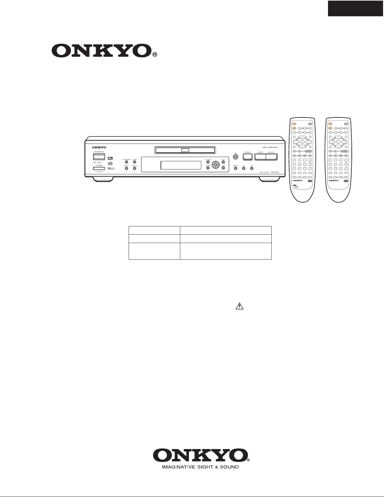
DV-S555
DV-S555
Ref. No.3685
072001
Black, Silver and Golden models
BMDD 120V AC, 60Hz
BMUP, SMUP 230 -240V AC, 50/60Hz
BMUT, BMUS,
GMUT, GMUR
100 - 240V AC, 50/60Hz
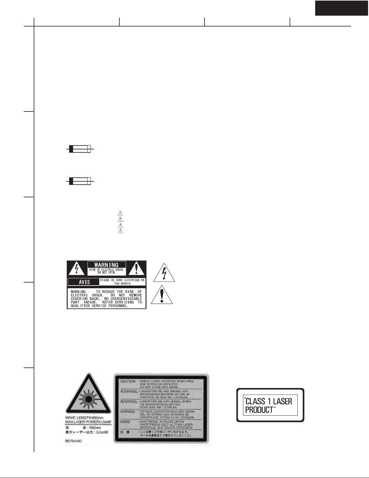
SAFETY-RELATED COMPONENT
WARNING!!
COMPONENTS IDENTIFIED BY MARK ON THE
SCHEMATIC DIAGRAM AND IN THE PARTS LIST ARE
CRITICAL FOR RISK OF FIRE AND ELECTRIC SHOCK.
REPLACE THESE COMPONENTS WITH ONKYO
PARTS WHOSE PART NUMBERS APPEAR AS SHOWN
IN THIS MANUAL.
MAKE LEAKAGE-CURRENT OR RESISTANCE
MEASUREMENTS TO DETERMINE THAT EXPOSED
PARTS ARE ACCEPTABLY INSULATED FROM THE
SUPPLY CIRCUIT BEFORE RETURNING THE
APPLIANCE TO THE CUSTOMER.
ON
OPEN/CLOSE
TV
ON/STANDBY
STANDBY
ANGLE AUDIO
SUBTITLE
LAST M COND.M DIMMER DISPLAY
MENU
TOP MENU
-
CH
+
VOL
ENTER
-
VOL
SETUP
RETURN
TV/VCR
STOPPAUSE
PLAY
DOWN UPFR FF
STEP/SLOW
23
1
456
FUNCTION M
789
CLEAR
SEARCH
+
10
0
PROGRAM
RANDOM REPEAT A-B
-
RC
449
DV
REMOTE CONTROLLER
TVDVD
RC-449DV RC-450DV
U.S.A., Canadian
models only
CH
+
-
+
STANDBY
LAST M COND.M DIMMER DISPLAY
TOP MENU
RETURN
TV/VCR
+
RANDOM REPEAT A-B
REMOTE CONTROLLER
Other models
ON
TV
ON/STANDBY
ANGLE AUDIO
-
CH
+
VOL
ENTER
-
VOL
STOPPAUSE
DOWN UPFR FF
23
1
456
789
SEARCH
10
0
-
RC
450
TVTVDVD
OPEN/CLOSE
SUBTITLE
MENU
+
CH
SETUP
PLAY
STEP/SLOW
+
-
FUNCTION M
CLEAR
PROGRAM
DV
Page 2

SPECIFICATIONS
DVD Player
Power supply North American models: AC 120 V, 60 Hz
Other models: AC 100 - 240 V, 50/60 Hz
Power consumption North American models: 14 W
Other models: 15 W
Weight 3.4 kg, 7.1 lbs.
External dimensions 435 x 91 x 312 mm (W/H/D), 17-1/8" x 3-9/16" x 12-5/16"
Signal system PAL/NTSC
Regional restriction code North American area: 1
Some Asian are: 3
South American area: 4
Chiness area: 6
Laser Semiconductor laser , wavelength 650 nm
Frequency range (digital audio) DVD linear sound: 48 kHz sampling 4 Hz to 22 kHz
96 kHz sampling 4 Hz to 44 kHz
Audio CD: 4 Hz to 20 kHz
Signal-to-noise ratio (digital audio) More than 100 dB
Audio dynamic range (digital audio) More than 96 dB
Harmonic distortion (digital audio) Less than 0.05 %
Wow and flutter Below measurable level (less than +/- 0.001 % (W.PEAK))
Operating conditions Temperature: 5 C to 35 C (41 F to 95 F), Operation status: Horizontal
DV-S555
Outputs
Video output 1.0 V (p-p), 75 ohm , negative sync., pin jack x 1
S-video output (Y) 1.0 V (p-p), 75 ohm , negative sync., Mini DIN 4-pin x 1
(C) 0.286 V (p-p), 75 ohm
Component video output (Y) 1.0 V (p-p), 75 ohm , negative sync., pin jack x 1
(P
B)/(PR) 0.7 V (p-p), 75 ohm <MDD/MUS/MUT/MUR>
RGB signal output, 0.7 V (p-p), 75 ohm , SCART socket x 1
Audio output (digital output Optical) Optical connecter x 1
Audio output (digital output Coaxial) 0.5 V (p-p), 75 ohm , pin jack x 1
Audio output (2-Channel Audio) 2.0 V (rms), 320 ohm , pin jack (L, R, MONO) x 1
Audio output (analog audio)
Specifications and features are subject to change without notice.
2.0 V (rms), 470 ohm, pin jack (L, R. MONO) x 1
<MUP>
Page 3
DV-S555
A
BCD
SERVICE NOTE
PRECAUTIONS
1
2
1.Ground for the work-desk.
Place a conductive sheet such as a sheet of copper (with impedance lower than 10Mohm) on the work-desk and
place the set on the conductive sheet so that the chassis.
2.Grounding for the test equipments and tools.
Test equipments and toolings should be grounded in order that their ground level is the same the ground of the power source.
3. Grounding for the human body.
Be sure to put on a wrist-strap for grounding whose other end is grounded.
Be particularly careful when the workers wear synthetic fiber clothes, or air is dry.
4. Select a soldering iron that permits no leakage and have the tip of the iron well-grounded.
5. Do not check the laser diode terminals with the probe of a circuit tester or oscilloscope.
1. Replacing the fuses
This symbol located near the fuse indicates that the
fuse used is show operating type, For continued protection against
fire hazard, replace with same type fuse , For fuse rating, refer to
the marking adjust to the symbol.
Ce symbole indique que le fusible utilise est e lent.
Pour une protection permanente, n'utiliser que des fusibles de meme
type. Ce demier est indique la qu le present symbol est apposre.
2. Safety-check out
(Only U.S.A. model)
After correcting the original service problem perform the
following safety check before releasing the set to the customer
Connect the insulating-resistance tester between the plug of
power supply cord and terminal GND on the back panel.
Specifications: More than 10M ohm at 500V
REF.NO.
F1
3
TO REDUCE THE RISK OF FIRE OR ELECTRIC SHOCK, DO NOT EXPOSE THIS APPLIANCE TO RAIN
WARNING :
4
OR MOISTURE. DANGEROUS HIGH VOLTAGES ARE PRESENT INSIDE THE ENCLOSURE. DO NOT OPEN THE
CABINET. REFER SERVICING TO QUALIFIED PERSONNEL ONLY.
CAUTION :
TO PREVENT ELECTRIC SHOCK, MATCH WIDE BLADE OF PLUG TO WIDE SLOT, FULLY INSERT.
POUR EVITER LES CHOCS ELECTRIQUE, INTRODUIRE LA LAME LA PLUS LARGE DA LA FICHE DANS LA
ATTENTION :
BORNE CORRESPONDANTE DA LA PRISE ET POUSSER JUSQU' AU FOND.
PART NO.
252152 or
252147
252273 or 1.6A-SE-TL250V or
252077 1.6A-SE-EAK Fuse
NOTE : <MDD> : 120 V model only
<MUP,MUS,MUT,MUR>
DESCRIPTION
1.6A-T/UL-ST2 or
1.6A-TSC, Fuse <MDD>
<MUP,MUS,MUT,MUR>
: 100 - 240 V model only
The lightning flash with arrowhead symbol, within an equilateral triangle, is
intended to alert the user to the presence of uninsulated "dangerous voltage"
within the product's enclosure that may be of sufficient magnitude to constitute
a risk of electric shock to persons.
The exclamation point within an equilateral triangle is intended to alert the user
to the presence of important operating and maintenance (servicing) instruction
in the literature accompanying the appliance.
5
Page 4
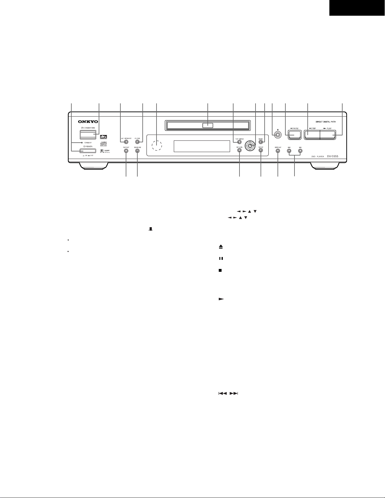
PANEL VIEW
Front panel
DV-S555
1 2 3 4 5
14 15
1. POWER switch and STANDBY indicator
Turns on the main power supply for the DV-S555. The DV-S555
enters standby state and the STANDBY indicator lights up.
Pressing the switch again to the off position ( OFF) shuts down
the main power supply into the DV-S555.
Before turning on the power, make sure all cables are properly
connected.
Turning on the DV-S555 may cause a momentary power
surge that might interfere with other electrical equipment on
the same circuit. If this is a problem, plug the DV-S555 into a
different electrical circuit.
2. STANDBY/ON button
When ST ANDBY/ON button is pressed to ON while the POWER
switch is set to ON, the DV-S555 turns on and the STANDBY
indicator turns off. Pressing the button again returns the DV-S555
to the standby state. This state turns of f the display , disables
control functions.
3.
LAST MEMORY button
You can resume DVD or Video CD playback from the point you
last watched even if the disc is removed from the player. Press
LAST MEMORY during playback to set a Last Memory point.
When you want to resume playback of that disc, press LAST
MEMORY in the stop mode and playback starts from the
memorized point. Last Memory locations can be stored for up to 5
DVDs and 1 V ideo CD.
4.
CLEAR button
Works in conjunction with a number of player functions. Use to
cancel repeat and random playback, and to edit programs.
5. Remote control sensor
Point the remote control toward the remote sensor to operate the
player .
Disc tray
6.
When loading a disc, place discs in the disc tray with the label
side facing up.
7.
TOP MENU button
Press to call up the top menu programmed on the DVD.
Depending on the DVD, the top menu may be identical to the
DVD menu.
6 8 9 10 11 12 13
8. Cursor (
7
16 17 18
) button/ENTER button
/ / /
(
Use to move through the options on menu screens and
to change settings. Use ENTER to implement settings selected
with the cursor buttons or to set items highlighted in a menu.
/ / /
)
19
9. MENU button
Use to display or close the DVD menu or MP3 Navigator screen.
OPEN/CLOSE button
10.
Press to open and close the disc tray.
11.
PAUSE button
Press during playback to pause. Press again to resume playback.
12.
STOP button
Press to stop playback. Pressing once enables playback to
resume from a point shortly before the location where it stopped.
Pressing twice causes the disc to return to the beginning of the
disc if playback starts again.
13.
PLAY button
Press to start or resume playback.
14.REPEAT button
Use to set the repeat mode.
15.RANDOM button
Press to play chapters/tracks in random order
16.
RETURN button
Use to go one menu back (current settings are maintained). Use
RETURN when you do not want to change the option setting in a
menu.
SETUP button
17.
Press when the player is in either play or stop mode to open and
close the Setup screen.
18.
DISPLAY button
Press during playback to display statistical disc information.
Press repeatedly to display different information.
19.
button
/
Press to go back or advance to previous chapters/tracks. Press
and hold to perform fast-reverse/fast-forward playback scanning.
.
Page 5
PANEL VIEW
Display
DV-S555
1 2 3 4 5 6 7 8 9
10 11 12 13
Rear panel
DVD VC D
D
DTS
GUI
/ indicator
1.
Inserted disc indicator
2.
TITLE indicator
3.
Angle icon indicator
4.
TITLE CHAPTER TRACK REMAIN
5. CHAPTER/TRACK indicator
6.
REPEA T indicator
7.
REMAIN indicator
1 2 3 4 5 6 7 8
VIDEO
S VIDEO
VIDEO
OUTPUT
COMPONENT
ANALOG
OUTPUT
MONO
Y
C
B
L
R
C
R
REPEAT
LAST indicator
8.
COND. indicator
9.
10.
11.
12.
13.
D indicator
DTS indicator
GUI indicator
Multifunctional indicator
LAST
COND.
(e.g. operating status and error messages)
DIGITAL
OUTPUT
REMOTE
OPTICAL
COAXIAL
CONTROL
DVD PLAYER
DV-S555
AC INLET
1.
VIDEO OUT VIDEO jack
Connect to the video input on a TV or monitor or AV amplifier or
receiver with video input capability .
2.
VIDEO OUT S-VIDEO OUT jack
If your TV or monitor has an S-video input, clear picture
reproduction is possible by connecting the player to your TV or
monitor via the S-Video jack.
You can switch between [S1] and [S2] S-video output from the
Setup menu.
3.
VIDEO OUT COMPONENT jacks
If your TV or monitor has component video inputs, you can
produce a higher quality picture on your TV or monitor by
connecting to the component video outputs on this unit.
4.
ANALOG OUTPUT jacks
Use to output two-channel audio (analog) to the audio stereo
inputs on a TV or stereo amplifier . If you are connecting to a
receiver that has both digital and analog input jacks for DVD
player connection, it may be beneficial to make both connections.
(North American models rear panel shown)
DIGITAL OUTPUT OPTICAL jack
5.
Use to output the digital audio signal recorded on discs.
output the digital signal via the optical output jack to an AV
amplifier or receiver .
DIGITAL OUTPUT COAXIAL jack
6.
Use to output the digital audio signal recorded on discs.
output the digital signal via the coaxial output jack to an AV
amplifier or receiver .
jack
7.
Use to connect this player to another component bearing the RI
mark. This lets you control this unit as though it were a
component in a system.
8.
AC INLET
Use to connect the power cord to the wall outlet.
ou can
Y
You can
Page 6

PANEL VIEW
Remote controller
DV-S555
TV
ON/STANDBY
ANGLE AUDIO
VOL
ENTER
VOL
STOPPAUSE
23
0
TVDVD
+
-
DOWN UPFR FF
SEARCH
RC
-
PLAY
449
OPEN/CLOSE
SUBTITLE
STEP/SLOW
FUNCTION M
PROGRAM
DV
MENU
SETUP
CLEAR
+
CH
+
-
ON button
1
11
14
1
2
3
4
5
6
7
8
9
ON
STANDBY
LAST M COND.M DIMMER DISPLAY
TOP MENU
-
CH
RETURN
TV/VCR
10
1
12
13
456
789
+
10
RANDOM REPEAT A-B
REMOTE CONTROLLER
Press to switch the player on.
2
STANDBY button
Press to put the player in standby.
3
ANGLE button
Some DVDs are recorded with various camera angle playback
options. Press ANGLE repeatedly to display different camera
angles.
4
LAST MEMORY button
You can resume DVD or Video CD playback from the point you
last watched even if the disc is removed from the player. Press
LAST MEMORY during playback to set a Last Memory point.
When you want to resume playback of that disc, press LAST
MEMORY in the stop mode and playback starts from the
memorized point. Last Memory locations can be stored for up to 5
DVDs and 1 V ideo CD.
COND. M button
5
You can store in memory the settings for up to 15 DVDs. Press
COND. M during DVD playback to memorize the settings.
6
TOP MENU button*
Press to call up the top menu programmed on the DVD.
Depending on the DVD, the top menu may be identical to the DVD
menu.
Cursor buttons (
7
/ / /
)*
VOL +/ buttons (North American models only)
Use to move through the options on menu screens and to change
settings.
8
RETURN button*
TV/VCR button (North American models only)
Use to go one menu back (current settings are maintained). Use
RETURN when you do not want to change the option setting in a
menu.
PAUSE button
9
Press to pause playback of a disc. Press again to resume
playback.
STOP button
10
Press to stop playback. Pressing once enables playback to
resume from a point shortly before the location where it was
stopped. Pressing twice causes the disc to return to the beginning
of the disc when playback starts again .
15
16
18
20
22
23
24
25
26
27
29
31
FR/FF / buttons
11
17
19
21
During playback of DVD and Video CD, press to perform fast
forward scanning or to perform fast reverse scanning of DVD
and Video CD. When a CD or MP3 is loaded, audio scanning is
performed.
Number buttons (1-9, 0, +10)*
12
Use to perform direct title/folder and chapter/track searches, and
to input numerical values.
13
RANDOM button
Press to play chapters/tracks in random order.
REPEAT button
14
Use to set the repeat mode.
OPEN/CLOSE button
15
Press to open or close the disc tray.
SUBTITLE button
16
Press repeatedly to select one of the subtitle languages
28
30
programmed on a DVD or to turn the subtitles off.
AUDIO button
17
Press repeatedly to select one of the audio languages
programmed on a DVD.
For Video CD, CD and MP3, each press changes the audio
output as follows.
Stereo 1L(Left) 2/R(Right)
DISPLAY button
18
Press during playback to display statistical disc information.
Press repeatedly to display different information.
19
DIMMER button
Toggle to control the lightness of the display
20
MENU button*
.
Use to display or close the DVD menu or MP3 Navigator screen.
21
ENTER button*
Use to implement settings selected with the cursor buttons or to
set items highlighted in a menu.
SETUP button*
22
Press when the player is in either play or stop mode to open and
close the Setup screen.
PLAY
23
Press to start or resume playback.
UP/DOWN
24
/
During playback, press to go back to a previous chapter/track
and to advance to the next chapter/track .
STEP/SLOW +/- buttons
25
Press STEP/SLOW + or - during playback to view still frame.
Press and hold STEP/SLOW + or during playback to view slow
-
playback. In still frame, press STEP/SLOW + to advance DVDs
and Video CDs frame by frame and STEP/SLOW to back up a
-
few frames at a time (DVD only).
FUNCTION M button
26
You can store in memory up to 5 settings. Press FUNCTION M to
memorize and recall the settings.
CLEAR button
27
Works in conjunction with a number of player functions. Use to
cancel repeat and random playback, and to edit programs.
SEARCH button
28
Press to perform a title/folder, chapter/track or elapsed time
search.
PROGRAM button
29
You can program titles, chapters, or tracks to play back in a
desired order . Programs can be a maximum of 24 steps.
Additionally, DVD programs for up to 24 discs can be stored in
the player's memory for future use.
A-B button
30
Press at the beginning and end of the section you want to repeat
or to mark a location you want to return to.
31
DVD/TV switch (North American models only)
(Buttons indicated with * are used for menu operation.)
Page 7

EXPLODED VIEW
03
DV-S555
53
53
F1
U10
51
53
53
53
53
E702
U8
E903
Z11
13
Z12
To DVD
Mechanism
U1
Z14
Z13
Z14
Z10
23
15
U5
13
U6
01
D
V
D
23
25
33
U3
31
17
37
U2
23
37
23
54*
35
E701
20
50*
S731
03
: Torque 1.6+/-0.5kgf
*
19
29
27
21
23
37
41
U9
03
05
07
09
11
07
03
05
23
45
49
43
49
Page 8

Page 9

EXPLODED VIEW (LOADING MECHANISM)
A
DV-S555
2
23
Daifree
GEM1036
15
14
Lubricating Oil
12
GYA1001
13
6
To DVDM
CN151
8
8
8
8
20
18
17
16
19
A
10
11
Lubricating Oil
GYA1001
9
1
LOADING MECHANISM ASSY PARTS LIST
REF.NO PART NO.
1 VNP1836 Loading PC board assy
2 VXX2782 Traverse mechanism assy-S
6 VDA1864 Flexible cable 26P
8 VEB1327 Float rubber
9 VEB1328 Belt
10 VNE2253 Stabilizer
11 VNL1917 Loading base
DESCRIPTION
REF.NO. PART NO.
DESCRIPTION
12 VNL1918 Float base DVD
13 VNL1919 Drive cam
14 VNL1921 Gear pulley
15 VNL1922 Loading gear
16 VNL1923 Drive gear
17 VNL1925 SW lever
18 VNE2251 Clamper plate
19 VNE2252 Bridge
20 VNL1924 Clamper
23 VNL1920 Tray
Page 10
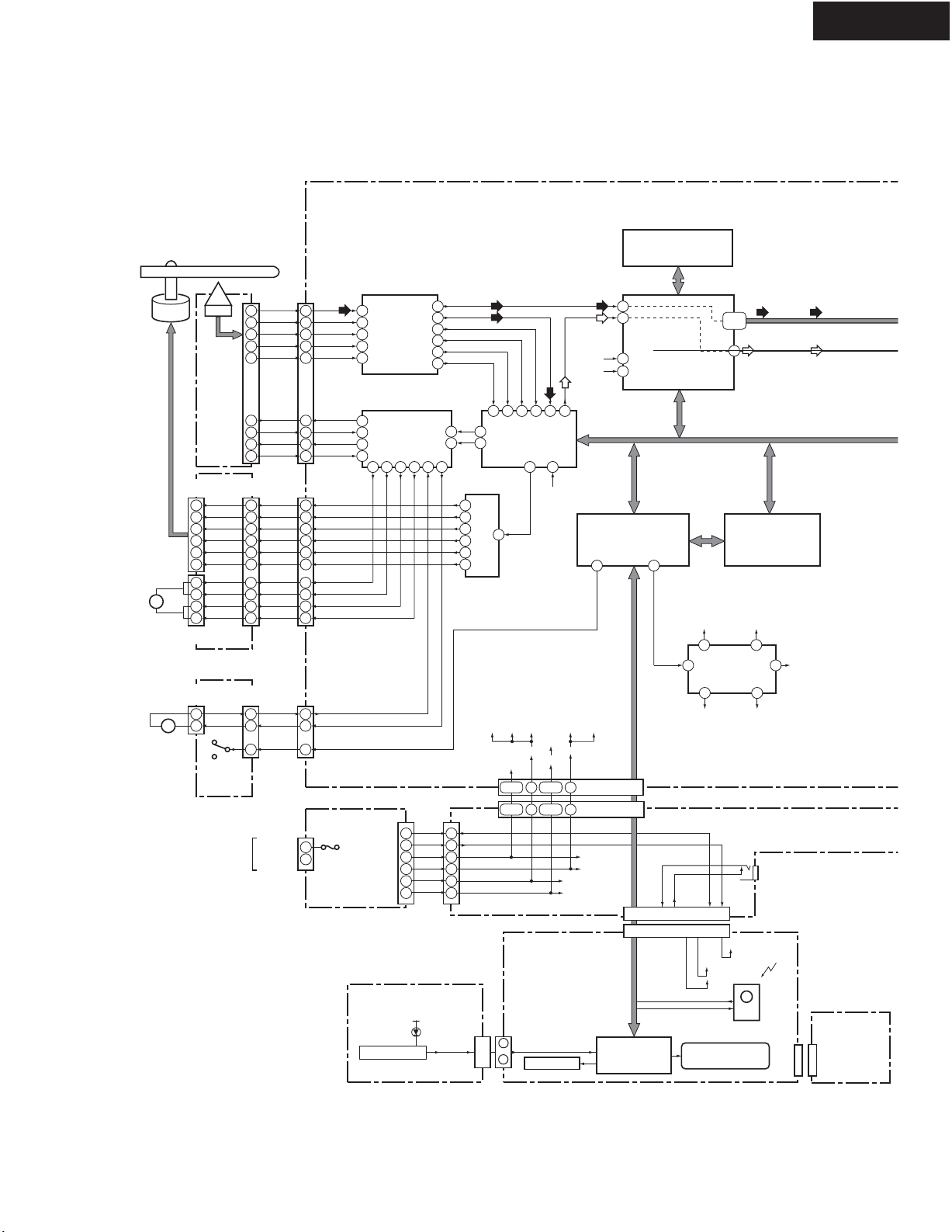
BLOCK DIAGRAM
Overall
DV-S555
Spindle
Motor
M
Stepping
Motor
(Carriage)
SSIB ASSY
CN602
+-
M
Loading
Motor
Assy
LOAB ASSY
Pickup
Assembly
CN1
(12P)
9
8
7
6
5
4
3
4
2
1
CN2
(4P)
(2P)
2
1
Loading
Position
Switch
S101
CN151
(26P)
RF
16
B1
7
B2
6
B3
12
B4
11
T DRV
2
T RTN
3
F DRV
4
F RTN
1
CN61
(17P)
H1+
9
H1-
10
H2+
11
H2-
12
H3+
13
H3-
14
ST1+
1
ST1-
2
ST2+
4
ST2-
5
CN52
(5P)
LOD- LOD-
1
LOD+ LOD+
2
SW2 LODPOS
4
CN1
(2P)
1
LIVE
F1
2
AC IN
(26P)
11
20
21
15
16
25
24
23
26
CN3
(17P)
9
10
11
12
13
14
1
2
4
5
CN601
(5P)
1
2
4
NEUTRAL
Main circuit PCB
DB-VPB301
(RF)
RF
3
B1
B2
B3
B4
T DRV
T RTN
F DRV
F RTN
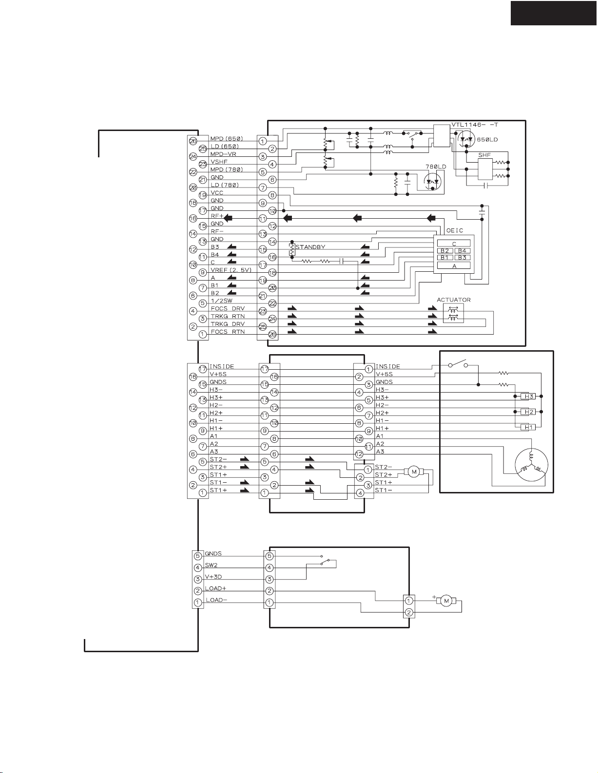
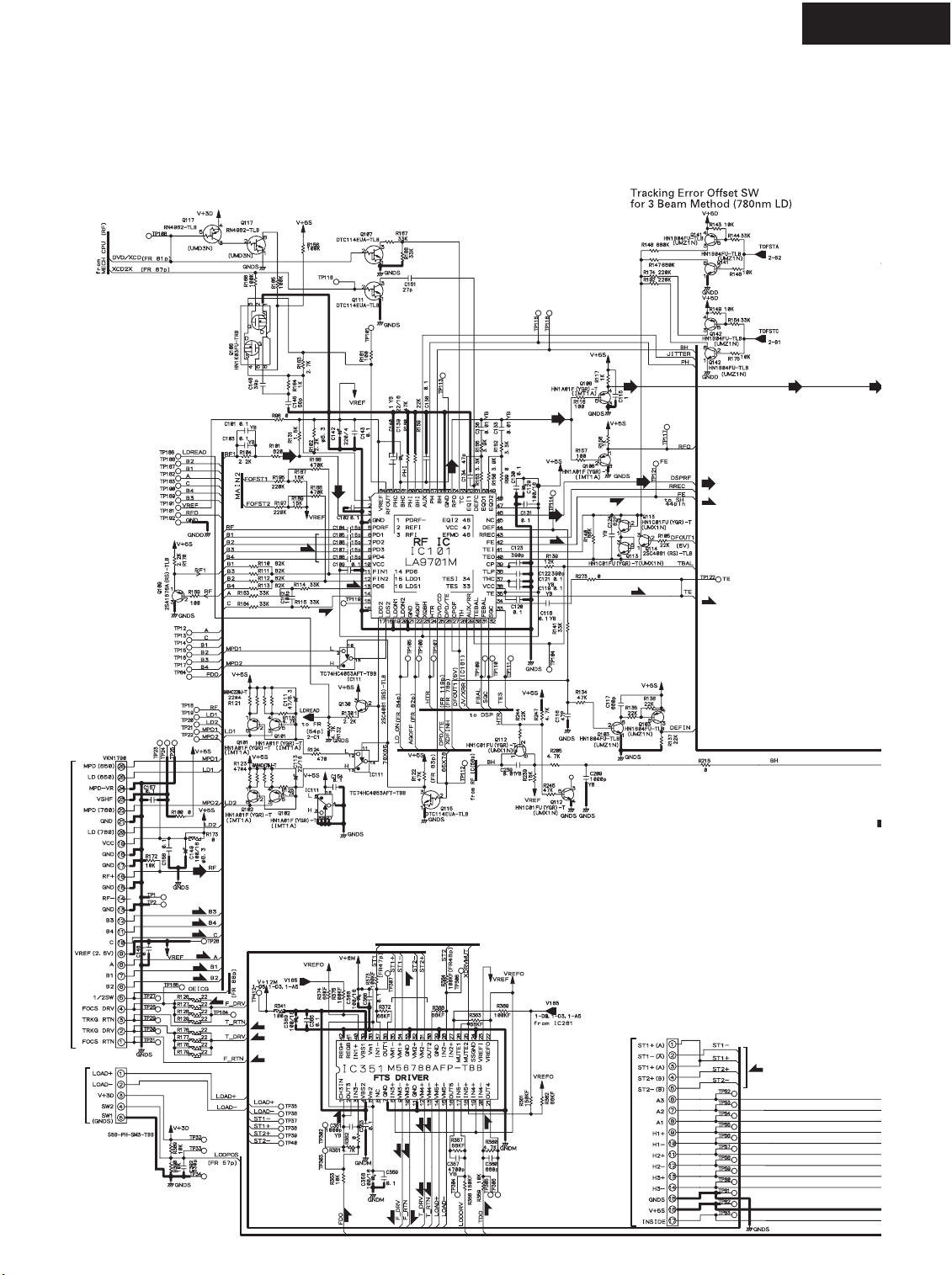
IC101
6
LA9701M
7
RF IC
8
9
12
IC351
13
M56788AFP
9
FTS Driver
10
35 34 31 32 15 14
CN2
(14P)
14
10
8
6
4
2
POWER
SUPPLY
UNIT
Standby PCB
NADIS-7183A
Key switck
-27V
EV+5V
+6V
+12V
+5V
+3.3V
54
46
56
57
42
35
DSP RF
3
20
1
5
7
9
11
13
JL771B
(RF) (RF)
RFO
(RF)
BH
PH
FE
TE
32 33 30 31 39 3
FDO
TDO
9
10
11
12
13
14
IC251
BA6664FM
Spindle
Driver
P902
(14P)
47
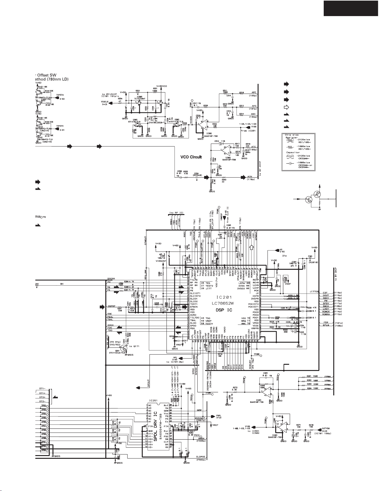
LC78652W
48
Servo DSP IC
SPDO
21
V+6M
28,30 21,23
1,3 8,10
-27V
EV+5V
IC201
46 14
V+5DV+5VV+5S
SW+5
29 22
2
Display circuit
NADIS-7182A
(5P)
JL771A
1
2
(5P)
KEY SW
(RF)
16M
V+3D
V3VD
PCB
ROMXA
(AD)
33M
16M
(AD)
System Control
57
LODPOS
V+12D V+12M
V12M
9
V+6M
V+12V
V+5V
V+3V
P701A
P701B
IC712
MSM51V17805D-60TS
16M DRAM
170
112
IC701
PE5108A
4
DVD Decoder
107
BY Chip
IC601
PD6345A
105
X48/44
X48/44
CONTROLCONTROLCONTROL
CN401 (2/2)
(30P)
CN102 (2/2)
(30P)
(22P)
(22P)
MPD780232GC
FL Control IC
SEL IR
Q701
(VD) (VD)
57-60
63-66
111
8M Flash Memory
27M
(for IC801)
(for IC201, IC701)
3
IC481
14 15
BU2288FV
Clock Generator
10
IR
IR
22/24M
(for IC211)
EV+5V
-27V
E+5V
-27V
FLAC2
FLAC1
Q702
FL Tube
36/16M
(for IC801)
SD0-SD7
CDDATA
IC603
VYW1853
16M
13
9
P354
CONTROL
Q705
Remote
Receiver
Unit
33M
(for IC701)
Jog switch
PCB
(7P)
(7P)
P731
P731
Page 11

CSCO
DV-S555
IC805
MB81F161622C-80FN
16M SDRAM
(VD)
149,150,
152-155,
158,159
48
IC801
M65774BFP
MPEG2 Decoder
AV-1
5564
27M36/16M
74
68
95-98,
100-103
(VD)
93
27M
(RF)
: RF SIGNAL ROUTE
(AD)
: AUDIO DATA SIGNAL ROUTE
: AUDIO SIGNAL ROUTE
(D)
: AUDIO (DIGITAL) SIGNAL ROUTE
(D)
(D)
DOUT0
ADA0A
PD0-PD7
24
2-9
48
28
25
35
33
29
IC861
(VD)
27M
ADV7172KST
Video Encoder
Cr/R
Cb/B
(VD)
: VIDEO DATA SIGNAL ROUTE
: VIDEO SIGNAL ROUTE
(V)
: V SIGNAL ROUTE
(Y)
: Y SIGNAL ROUTE
CN401 (1/2)
(30P)
DOUT0
(D) (D) (D)
CN15
(30P)
22/24M
Q911
Y/G
Q912
V
Q901
Y
C
Q903
Q913
Q902
29
27
25
26
30
28
DOUT
5 26
ADATA0
7
2
Cr/R
Y/G
Cb/B
V
Y
C
CN102 (1/2)
(30P)
CN106
(30P)
7
22/24M
2
Cr/R
29
Y/G
27
Cb/B
25
26
30
28
Q301
PCM1742KE
192kHz, 24bit
2ch DAC
7
2
(R)
(Y)
(B)
V
(V)
(Y)
Y
C
(C)
MM1540BF
Driver with LPF
8
6ch Amp.
16
13
9
11
2
6
4
Q201
(C)
: C SIGNAL ROUTE
(R)
: R SIGNAL ROUTE
(G)
: G SIGNAL ROUTE
(B)
: B SIGNAL ROUTE
(D)
Q601
Q401/402
NJM4565M-D
(V)
V
27
(Y)
Y
23
C
(C)
25
Cr/R
16
Y/G
20
Cb/B
18
AUDIO_L
AUDIO_R
(R)
(G)
(B)
Q352
OPTICAL
COAXIAL
P353
DIGITAL
(D)
JA201
L
AUDIO
R
Mono
(Y)
P201
Y
C
(C)
V
C
Y
R
G
B
S VIDEO
V
COMPOSITE
Composite
P203
(22P)
Video
component
(20P)
h
Output terminal PCB
P250B
(20P) (21P)
AUDIO_L
AUDIO_R
18
V
(V) (V)
7
(Y) (Y)
Y
5
(C)
C
3
13
9
11
1
(R)
R
(G)
G
(B)
B
15
2
Q251
TC4053BF
SCART terminal PCB <MUP> only
NAETC-7187A
NAAR-7181
5
4
3
(R/C)
(V) (V)
(G)
(B)
Q251
TC4053BF
(V/Y)
(R/C)
(G)
(B)
(R/C)
P251
(V/Y)
(G)
Scart
terminal
316
1
19
15
11
7
L OUT
R OUT
V/Y OUT
R/C OUT
G OUT
B OUT
P250A
Audio
Page 12
BLOCK DIAGRAM
Mechanism section
CN120
DV-S555
PICKUP ASSY-S
(RF) (RF) (RF) (RF)
CN251
DVDM ASSY
CN52
(F)
(F)
(T)
(T)
(F)
(F)
(F)
(T)
(T)
(F)
CN1
VKN1272
(S)
(S)
(S)
(S)
CN3
VKN1277
(S)
(S)
(S)
(S)
VKN1264
(F)
(T)
(T)
(F)
CN2
(F)
(F)
(T)
(T)
(F)
(F)
(F)
(T)
(T)
(F)
STEPPING MOTOR
(CARRIAGE)
: VXM1090
SPINDLE MOTOR
: VXM1088
SSIB ASSY
(VWG2292)
S101
: VSK1011
CN601
S5B-PH-K
LOAB ASSY
CN602
S2B-PH-K
LOADING
MOTOR
ASSY
: VXX2505
Page 13
SCHEMATIC DIAGRAM (Page 1)
To Spindle motor
Main circuit PC board
DV-S555
Page 2
Page 2
CN151
Page 2
(RF)
(V) (V)
(V)
(RF)
(F)
(T)
(T)
(V)
(A)
(F)
(A)
(F)
(T)
(A)
(F)
(T)
(V)
(A
PICKUP ASSY
CN601
CN52
Load PCB
For Mecha
connector
(RF)
(F)
(F)
(T)
(T)
(F)
(F)
Page 2
(F)
(T)
(T)
(F)
(F)
(F)
(S)
(S)
To Spindle motor
(T)
(T)
(F)
(F)
(T)
(T)
(F)
(F)
(T)
(T)
Page 14
Page 2
T
10
Page 2
Page 3
0.01
TC7SZU04F
IC304
470
100k
DV-S555
(RF)
: RF SIGNAL ROUTE
(V)
82k
15p
1k
3.3k
10k
22k
: RF (VIDEO) SIGNAL ROUTE
(A)
: RF (AUDIO) SIGNAL ROUTE
(AD)
: AUDIO DATA SIGNAL ROUTE
(F)
: FOCUS SERVO LOOP LINE
(T)
: TRACKING SERVO LOOP LINE
(S)
: SLIDER SERVO LOOP LINE
(V)
(V)
Page 3
)
F)
(V) (V)
DF OUT
From DSP IC
V+5V
3V to 5Volt
Q171
RN4982-TLB
4
(UMD3N)
5
6
54p
1
3
2
Page 1
to RF IC (IC 101)
28p
Page 2
)
Page 2
(AD)
From FR CPU
Page 3
(T)
(F)
(A)
(T)
(F)
5
(A)
Page 2
FR CPU
(F)
(T)
Page 3
BY CHIP
(F)
(T)
8 9
To Q171
(S)
7
Page 2
FR CHIP (IC601)
Page 3
BY CHIP (IC701)
162p
111110
Page 3
Page 15
SCHEMATIC DIAGRAM (Page 2)
VYW1853
DV-S555
Page 3
Page 1
Page 1
470k
Page 1
Page3
Page3
page 4
To CN15
CN512
MECHA
Page1
To CN15
Page 4
Video encoder
IC861 45p
page 4
page 1 IC201
Page 16
Page 2
T
10
Page 2
Page 3
0.01
TC7SZU04F
IC304
470
100k
DV-S555
(RF)
: RF SIGNAL ROUTE
(V)
82k
15p
1k
3.3k
10k
22k
: RF (VIDEO) SIGNAL ROUTE
(A)
: RF (AUDIO) SIGNAL ROUTE
(AD)
: AUDIO DATA SIGNAL ROUTE
(F)
: FOCUS SERVO LOOP LINE
(T)
: TRACKING SERVO LOOP LINE
(S)
: SLIDER SERVO LOOP LINE
(V)
(V)
Page 3
)
F)
(V) (V)
DF OUT
From DSP IC
V+5V
3V to 5Volt
Q171
RN4982-TLB
4
(UMD3N)
5
6
54p
1
3
2
Page 1
to RF IC (IC 101)
28p
Page 2
)
(AD)
Page 2
From FR CPU
Page 3
(T)
(F)
(A)
(T)
(F)
5
(A)
Page 3
BY CHIP
(F)
(T)
Page 2
FR CPU
(F)
(T)
8 9
To Q171
(S)
7
Page 2
FR CHIP (IC601)
Page 3
BY CHIP (IC701)
162p
111110
Page 3
Page 17

SCHEMATIC DIAGRAM (Page 3)
DV-S555
(VD)
***
C742
C705
***
(VD)
(V)
220/4
IC712
4M MSM51V17805D-60TS (SOP)
To SCRUT 7,21, 68, 188P
to CN15 page 4
Page 1 IC201
Page 1
R334
to CN401
Page 2/ IC601
Page 2/ IC601
Page 2/ IC601
Page 3 IC 801
Page 1 IC 201
(AD)
(AD)
Page 2 IC 601
(V)(V)
Page 1
to Page 1
Page 18
SCHEMATIC DIAGRAM (Page 3)
PAL model only
IC806
(V)
: RF (VIDEO) SIGNAL ROUTE
(VD)
: VIDEO DATA SIGNAL ROUTE
(AD)
: AUDIO DATASIGNAL ROUTE
: AUDIO SIGNAL ROUTE
(D)
: AUDIO (DIGITAL) SIGNAL ROUTE
DV-S555
(VD)
from AV1 88p IC801
(VD) (VD)
DCS2
Page 2
IC801
(VD)
(D)
(D)
from Clock generator Page 2
MAIN/ADDRESS/DATA from FR30 Page 2 IC601
from Clock generator Page 2
from SCRUT Page 3 IC701
Page 2 IC601
Page 19
SCHEMATIC DIAGRAM (Page 4)
DV-S555
from AV 1 MPEG decoder
(IC801)
page 3
(VD) (VD)
Page 2
FR CPU 101p
(V) (V)
(Y)
(C) (C)
(V)
(Y)
(C)
(V)
(Y)
(C)
(R)
(B)
(Y)
(R)
(G)(G)
(B)
Page 2
Page 20

(VD)
: VIDEO DATASIGNAL ROUTE
(V)
: V SIGNAL ROUTE
(Y)
: Y SIGNAL ROUTE
(C)
: C SIGNAL ROUTE
(R)
: R SIGNAL ROUTE
(G)
: G SIGNAL ROUTE
(B)
: B SIGNAL ROUTE
: AUDIO SIGNAL ROUTE
DV-S555
(V)
(V)
(Y) (Y)
(C)
(R)
(G)
(G)
(B)
page 2
FR CPU
(V)
(R)
(R)
(G)
page 3
(Y)
(R)
(C)
(G)
(V)
(B)
(B)
(R)
(G)
(Y)
(C)
(V)
(B)
CN15
CN106
Page 21

DV-S555
DV-S555
A
BCDEFGH
SCHEMATIC DIAGRAMS
P701A
SCK
22
232SO
21
SI
1
2
P/XI[VSEL2]
3
232SCK
SO
232SI
XRDY
232BU
PON
232RE
RESET
RI
LT1
GND2
VCOFF
GND1
EVER+5V
-27V
FLAC1
FLAC2
NC
SRESET
CN106
GND1
MCLK
BCK
GND2
LRCK
XCSDF
ADATA0
XSCK
ADATA1
XSI
ADATA2
6CH/X2CH
ADATA3
XMUTE
VSEL1
LFE_ON
GND3
PRG_CR
GND4
PRG_CB
GND5
PRG_Y
GND6
B/CB
G/Y
R/CR
20
19
18
17
16
15
14
13
12
11
10
9
8
7
6
5
4
3
2
1
1
2
3
4
5
6
7
8
9
10
11
12
13
14
15
16
17
18
19
20
21
22
23
24
25
V
26
27
C
28
29
Y
30
CN102
M+6V1
1
SW5V
2
M+6V2
3
GND1
4
GNDM1
5
GND2
6
GNDM2
7
+3.3V1
8
9
+12VM
+3.3V2
10
GND3
11
+2.5V1
12
+2.5V2
13
GND4
4
GND5
MICON2
MICON1
CTS
LT1
DTR
XRESET
RXD
S[FTOM]
TXD
S[MTOF]
AODAI
SCK
SQUEEZE
XREADY
LETTER
14
15
16
17
18
19
20
21
22
23
24
25
26
27
28
29
30
P104
1
5
TXD
RXD
DTR
CTS
V+5D
GNDD
NC
2
3
4
5
6
7
Output Terminal PC board
SCK
232SO
SI
232SCK SW+5V
SO
232SI
XREADY
232BU
P_ON SQUEEZE
232RE
XRESET
RI
LT
GND
VCOFF
GND
EVER+5V
-27V
FLAC1
FLAC2
232RESET V V+8V
R102
47
MCLK
47
R103
BCK
R104
47
LRCLK Y
R105
47
XCSDF
R106
47
ADATA0
R107
47
XSCK
R108
47
XSI
R109
47
XMUTE
R110
47
VSEL1
47
R111
VSEL2 R/CR
R112
47
B/CB C1
R113
47
V
47
R114
R115
R116
R117
R118
R119
R120
R121
R122
R123
R124
R125
R126
R127
R128
R129
R130
G/Y Y1
47
C
47
R/CR V1
47
Y
47
47
47
47
XRESET
47
47
47
47
47
DOUT
47
47
SQUEEZE
47
XREADY
47
LETTER
10K
10K
10K
R134 10K
R133
R132
R131
1mm Pich FFC
For Download
NAAR-7181
10K
R101
DOUT
R135
R136
R137
R138
Q902
025EZ5M
VOUT
GND
C915
104Z
5NC4
3
C901
104Z
C903
104Z
C905
CTS
LT
DTR
RXD BCK MCLK
SO ADATA0 XCSDF
TXD LRCLK XSCK
SI XSI
SCK
TXD
RXD
DTR
CTS
C101
104Z
104Z
C907
104Z
P351BP351A
232SO
ON/OFF2VIN
1
-27V
FLAC1
232SCK
C902
220/16
C904
220/6.3
C906
220/16
C908
220/6.3
FLAC2
232SI
P_ON
L351
R357
0
C351
232BU
GND
EVER+5V
BK1608LM182-T
104Z
C352
P710B
SI
GND
M+5V
MGND
V+12V
470K
100/6.3
R351 100K
C353
R352
GND
for FL Micon DL
SO
SCK
P711
C909
104Z
C910
220/6.3
GND
GND
SW+5V
+3.3V
P902
Q351
TC74VHCU04T
GND
EVER+5V
C361
020
13
VCC14
12345
R901
C301
100/6.3
9
101112
6
0
XMUTE
C302
104Z
C303
100/6.3
C304
104Z
C354
R353
8
GND7
C362
020
232RE
330
104K
R354
L352
BK1608LM182-T
C911
100/16
BCKIN1
MCLK
DATA2
LRCKIN3MC
GND4
ZEROL
VDD5
VCC6
ZEROR
VOUTL7
VCOM
VOUTR8
AGND
Q301
PCM1742KE
232BU
232SI
232SO
232SCK
232RESET
P751A
180
I
ML
MD
R355
R356
470
Q901
78M08
G
16
15
14
13
12
11
10
9
220
180
C355
C356
104Z
223Z
C359
BK1608LM182-T
O
C912
R433
1K
R434
C357
C358
C360
L353
R902
10K
100/16
RN 1407
R301
220
RN1407
100/6.3
223Z
Q302
Q303
3
2
1
V+12V
D901
UDZS5.1B
C305
2
3
SW+5V
100/6.3
C913
P353
COAXIAL_OUT
OPTICAL_OUT
GP1FA551RZ
Q352
P354
C914
47/16
D401
1SS352
AGND
C306
104Z
D402
1SS352
RI_OUT1
104Z
V+6A
MUTE+12V
V+12V
MUTE+12V
C401
22/50
C402
22/50
1.8K
C452
R431
NC
R435
R403
R404
R436
RN1407
R401
2.2K
R402
2.2K
RN1407
Q419
C403
C404
Q410
LETTER
C201
R405
15K
R406
15K
C
G/Y
B/CB
100/16
R437
C405
C406
R438
C202
R407
10K
221
221
R408
10K
104Z
Q411
2SA1162
R409
33K
2
3
R411
R412
3
2
R410
33K
4.7K
Q412
2SA1162
C203
104Z
C204
104K
C205
C206
104K
C207
104K
C208
C209
104K
C210
10/6.3
C211
104K
C212
C213
104K
C214
C417
C407
330
NJM4565M-D
+B
8
0
100/16
0
100/16
8
+B
NJM4565M-D
C408
330
102
C418
C225
C215
Q401
C409
C410
Q402
104Z
R289
R290
47/16
1
1
Q202
RN1407
100K
100K
104Z
C216
R MP OTHERS
R224 0 NC
R225 0 NC
R226 0 NC
R227 0 NC
R228 0 NC
R229 0
R415
C411
220
22/50
HN1C03F
Q403
100K
R413
100K
R414
Q404
HN1C03F
C412
R416
22/50
220
5
2.2K
C413
102
C414
102
2.2K
5
20
3
4
4
3
Q451
RN1407
R203
Q403
HN1C03F
Q404
HN1C03F
Q205
RN2403
0
R423
1K
R424
1K
Q204
RN1407
Q203
RN2403
1.5K
R201
1K
R202
VCC11VCC228
VIN2VOUT27
PS126
YCMIX3
CIN4
COUT25
VEE624
CLP5
YIN16
YOUT123
Q201MM1540BF
MUTE17
VEE522
MUTE28
VEE421
YIN29
YOUT2
GND10
VEE319
CBIN11 CBOUT18
DUAL12
PS217
CRIN13 CROUT16
VEE114 VEE215
NC
R419
220
6
2
R421
1
2.2K
R417
R418
2.2K
1
R422
2
6
R420
220
R452
R451R432
R224
R225
6
5
5
6
R453
R226
-B
-B
R227
4
4
2SA1162
C220
R211
470/6.3
C221
R214
470/6.3
C222
R219
470/6.3
R229
R228
R441
1K
R425
7
Q401
NJM4565M-D
Q402
NJM4565M-D
R426
7
R442
1K
C451
Q452
R206
10K
C218
470/6.3
C219
104K
C217
470/6.3
0
0
0
470
470
R212
75
R215
100
R220
100
R217
R222
C415
22/50
R207
R209
R204
470
470
75
75
75
R208
L202
L
L
R210
L
R205
R213
L204
L
R216
L205
L
560
R218
R221
L206
L
560
R223
R428
100K
HN1C03F
Q405
2
R454
220
R429
2.2K
L203
L201
1
HN1C03F
6
R430
Q405
5
R455
220
2.2K
P201
1
3
5
4
2
6
7
8
4
2
1
3
V+12V
VSEL1
VSEL2
GND
G1
B1
R1
SQUEEZE
4
3
2
1
3
3
1
2
4
P203
P250A
V+12V
1
VSEL1
2
C
3
VSEL2
4
5
Y
GNDV1
6
V7
GNDV2
8
G
9
GNDV3
10
B11
GNDV4
12
R
13
GNDV5
14
15
+5V
AUDIO_L
16
GNDA
17
AUDIO_R
18
SQUEEZE
19
V+8V
20
P402
P401
G1
Y
G2
C
G3
SW
G4
SIGNAL
Y
CB
GND
CR
L
R
MONO
L
R
Page 22

DV-S555
A
BCDEFGH
SCHEMATIC DIAGRAMS
P701A
SCK
22
232SO
21
SI
1
2
P/XI[VSEL2]
3
232SCK
SO
232SI
XRDY
232BU
PON
232RE
RESET
RI
LT1
GND2
VCOFF
GND1
EVER+5V
-27V
FLAC1
FLAC2
NC
SRESET
CN106
GND1
MCLK
BCK
GND2
LRCK
XCSDF
ADATA0
XSCK
ADATA1
XSI
ADATA2
6CH/X2CH
ADATA3
XMUTE
VSEL1
LFE_ON
GND3
PRG_CR
GND4
PRG_CB
GND5
PRG_Y
GND6
B/CB
G/Y
R/CR
20
19
18
17
16
15
14
13
12
11
10
9
8
7
6
5
4
3
2
1
1
2
3
4
5
6
7
8
9
10
11
12
13
14
15
16
17
18
19
20
21
22
23
24
25
V
26
27
C
28
29
Y
30
CN102
M+6V1
1
SW5V
2
M+6V2
3
GND1
4
GNDM1
5
GND2
6
GNDM2
7
+3.3V1
8
9
+12VM
+3.3V2
10
GND3
11
+2.5V1
12
+2.5V2
13
GND4
4
GND5
MICON2
MICON1
CTS
LT1
DTR
XRESET
RXD
S[FTOM]
TXD
S[MTOF]
AODAI
SCK
SQUEEZE
XREADY
LETTER
14
15
16
17
18
19
20
21
22
23
24
25
26
27
28
29
30
P104
1
5
TXD
RXD
DTR
CTS
V+5D
GNDD
NC
2
3
4
5
6
7
Output Terminal PC board
SCK
232SO
SI
232SCK SW+5V
SO
232SI
XREADY
232BU
P_ON SQUEEZE
232RE
XRESET
RI
LT
GND
VCOFF
GND
EVER+5V
-27V
FLAC1
FLAC2
232RESET V V+8V
R102
47
MCLK
47
R103
BCK
R104
47
LRCLK Y
R105
47
XCSDF
R106
47
ADATA0
R107
47
XSCK
R108
47
XSI
R109
47
XMUTE
R110
47
VSEL1
47
R111
VSEL2 R/CR
R112
47
B/CB C1
R113
47
V
47
R114
R115
R116
R117
R118
R119
R120
R121
R122
R123
R124
R125
R126
R127
R128
R129
R130
G/Y Y1
47
C
47
R/CR V1
47
Y
47
47
47
47
XRESET
47
47
47
47
47
DOUT
47
47
SQUEEZE
47
XREADY
47
LETTER
10K
10K
10K
R134 10K
R133
R132
R131
1mm Pich FFC
For Download
NAAR-7181
10K
R101
DOUT
R135
R136
R137
R138
Q902
025EZ5M
VOUT
GND
C915
104Z
5NC4
3
C901
104Z
C903
104Z
C905
CTS
LT
DTR
RXD BCK MCLK
SO ADATA0 XCSDF
TXD LRCLK XSCK
SI XSI
SCK
TXD
RXD
DTR
CTS
C101
104Z
104Z
C907
104Z
P351BP351A
232SO
ON/OFF2VIN
1
-27V
FLAC1
232SCK
C902
220/16
C904
220/6.3
C906
220/16
C908
220/6.3
FLAC2
232SI
P_ON
L351
R357
0
C351
232BU
GND
EVER+5V
BK1608LM182-T
104Z
C352
P710B
SI
GND
M+5V
MGND
V+12V
470K
100/6.3
R351 100K
C353
R352
GND
for FL Micon DL
SO
SCK
P711
C909
104Z
C910
220/6.3
GND
GND
SW+5V
+3.3V
P902
Q351
TC74VHCU04T
GND
EVER+5V
C361
020
13
VCC14
12345
R901
C301
100/6.3
9
101112
6
0
XMUTE
C302
104Z
C303
100/6.3
C304
104Z
C354
R353
8
GND7
C362
020
232RE
330
104K
R354
L352
BK1608LM182-T
C911
100/16
BCKIN1
MCLK
DATA2
LRCKIN3MC
GND4
ZEROL
VDD5
VCC6
ZEROR
VOUTL7
VCOM
VOUTR8
AGND
Q301
PCM1742KE
232BU
232SI
232SO
232SCK
232RESET
P751A
180
I
ML
MD
R355
R356
470
Q901
78M08
G
16
15
14
13
12
11
10
9
220
180
C355
C356
104Z
223Z
C359
BK1608LM182-T
O
C912
R433
1K
R434
C357
C358
L353
100/16
Page 23

223Z
C357
C358
C360
L353
R902
10K
100/16
RN 1407
R301
220
RN1407
100/6.3
223Z
Q302
Q303
3
2
1
V+12V
D901
UDZS5.1B
C305
2
3
SW+5V
100/6.3
C913
P353
COAXIAL_OUT
OPTICAL_OUT
GP1FA551RZ
Q352
P354
C914
104Z
47/16
D401
1SS352
AGND
C306
104Z
D402
1SS352
RI_OUT1
V+6A
MUTE+12V
V+12V
MUTE+12V
1.8K
C452
C401
22/50
C402
22/50
R431
NC
R435
R403
R404
R436
RN1407
R401
2.2K
R402
2.2K
RN1407
Q419
C403
C404
Q410
LETTER
C201
R405
15K
R406
15K
C
G/Y
B/CB
100/16
R437
C405
C406
R438
C202
R407
10K
221
221
R408
10K
104Z
Q411
2SA1162
R409
33K
2
3
0
R411
0
R412
3
2
R410
33K
4.7K
Q412
2SA1162
C225
C203
104Z
C204
104K
C205
C206
104K
C207
104K
C208
C209
104K
C210
10/6.3
C211
104K
C212
C213
104K
C214
C215
C417
C407
330
NJM4565M-D
Q401
+B
8
C409
100/16
C410
100/16
8
+B
Q402
NJM4565M-D
C408
330
102
C418
104Z
Q202
RN1407
R289
100K
R290
100K
47/16
R MP OTHERS
R224 0 NC
R225 0 NC
R226 0 NC
R227 0 NC
R228 0 NC
R229 0
C411
22/50
1
1
C412
22/50
Q204
RN1407
Q203
RN2403
1.5K
R201
1K
R202
VCC11VCC228
VIN2VOUT27
YCMIX3
CIN4
CLP5
YIN16
MUTE17
MUTE28
YIN29
GND10
CBIN11 CBOUT18
DUAL12
CRIN13 CROUT16
VEE114 VEE215
104Z
C216
NC
R415
220
6
HN1C03F
Q403
2
1
100K
R413
2.2K
R417
R418
2.2K
1
100K
R414
2
Q404
HN1C03F
6
R416
220
R451R432
PS126
COUT25
VEE624
YOUT123
Q201MM1540BF
VEE522
VEE421
YOUT2
20
VEE319
PS217
R419
220
5
R421
2.2K
C413
102
C414
102
R422
2.2K
5
R420
220
RN1407
R452
R203
3
4
4
3
Q451
Q205
RN2403
0
R225
R224
6
R423
5
1K
Q403
HN1C03F
Q404
HN1C03F
R424
5
1K
6
R226
R453
R227
-B
-B
C220
470/6.3
C221
470/6.3
C222
470/6.3
R229
R228
R441
1K
7
Q401
4
NJM4565M-D
Q402
NJM4565M-D
4
7
R442
1K
C451
2SA1162
Q452
R206
10K
C218
470/6.3
C219
104K
C217
470/6.3
R211
0
R214
0
R219
0
R425
470
R426
470
R212
75
R215
100
R220
100
R217
R222
C415
22/50
R207
75
R209
75
R204
75
470
470
R208
L202
L
L
R210
L
R205
R213
L204
L
R216
L205
L
560
R218
R221
L206
L
560
R223
R428
100K
HN1C03F
Q405
2
R454
220
R429
2.2K
L203
L201
1
HN1C03F
6
R430
Q405
5
R455
220
2.2K
P201
1
3
5
4
2
6
7
8
4
2
1
3
V+12V
VSEL1
VSEL2
GND
G1
B1
R1
SQUEEZE
4
3
2
1
3
3
1
2
4
P203
P250A
V+12V
1
VSEL1
2
C
3
VSEL2
4
5
Y
GNDV1
6
V7
GNDV2
8
G
9
GNDV3
10
B11
GNDV4
12
R
13
GNDV5
14
15
+5V
AUDIO_L
16
GNDA
17
AUDIO_R
18
SQUEEZE
19
V+8V
20
P402
P401
G1
Y
G2
C
G3
SW
G4
SIGNAL
Y
CB
GND
CR
L
R
MONO
L
R
DV-S555
Page 24

DV-S555
DV-S555
A
SCHEMATIC DIAGRAMS
Display circuit PC board
1
2
3
4
5
NADIS-7182A
VOF_L
STB_L
MSO_0
FL_ON/OFF ENTER
40
39
2S
Q724
R780
VLED
192LED
41
96LED
42
PLYLED
43
STPLED
44
OPCLED
45
LEDO
46
NC5
47
NC6
48
NC7
49
P15
50
P14
51
P13
52
P12
53
P11
54
P10
55
P9
56
P8
57
P7
58
VDD2
59
VLOAD
60
P6P5P4P3P2
FL_ON/OFF
MSO_038MSO_137MSO_2
STBYLED
61
F1 48
.
THE COMPONENTS IDENTIFIED
REPLACE ONLY
.
VOLTAGE (MEASURED WITHVOLTMETER) IS
.
.
.
.
.
192_L K2
96_L INIT1
PLY_L SYSOUT
STP_L VCOFF
OPC_L LT1
R785
P15 PON
P14 XRDY
P13 SO
P12 SI
P11 XSCK
P10
P9
P8
P7
Q723
0
R552
2S
R781
BCDEFGH
Destination
MJJ2N
MDD1N
MUP2P
MUT3P
MUS4P
MUR6P
R790
10K
R789
10K
MSO_1
MSO_2
232SO
SRESET
R759
R713
0
0
36
34
35
32
33
NC3
NC4
TEST
R232SO
Q701
MPD780232GC
P1
P265P364P463P562P6
67
66
P1
14G
13G
12G
P15
P14
P13
P12
P11
P10
P10 39
P11 40
P12 41
P13 42
P14 43
P15 44
NOTE
ELECTROLYTIC CAPACITORS (
ALL CAPACITORS ARE IN pF/50WV UNLESS OTHERWISE NOTED.
EX) 030 3pF 330 33pF 331 330pF
ALL RESISTORS ARE IN OHMS 1/4WATTS
THE THICK LINES ON PC BOARD ARE THE PRINTING SIDE OF THE PARTS.
EX) PRINTING SIDE
CIRCUIT IS SUBJECT TO CHANGE FOR IMPROVEMENT.
R721R720
0
-
10K 56K
5.6K8.2K
33K
5.6K
68K
27K
5.6K33K
232SI
232BU
232RE
232SCK
R712
R7110
0
31
R232SCK
11G
10G
P9P8P7P6P5P4P3P2P1
38
P9
WITH PART
SYSIN
SYSOUT
R788
10K
R709
R710
0
0
29
28
30
R232SI
10G7111G7012G6913G6814G
P8 37
26
27
25
VDD0
SYSIN
SYSOUT
R232REQ
R232BUSY
9G
73
72
9G8G7G6G5G4G3G2G1G
P3 32
P4 33
P5 34
P6 35
P7 36
MARKBY
NUMBER SPECIFIED.
1K
R725
R727R726
0
K0
24
23
K022K1
+5V
VSS0
VCOFF
SYSRESET
RESET
P1 30
P2 31
MSO_0
K1
21
K2
INIT1
GND2
LT1
IRIN
NC2
NC1
PON
XRDY
SO
SI
XSCK
GND1
X1
X2
VSS1
VDD1
1G802G793G784G775G766G757G748G
Q702
0
20
19
18
17
16
15
14
13
12
11
10
9
8
7
6
5
4
3
2
1
R724
MSO_1
104Z
C702
14G
13G
12G
11G
12G16
13G17
14G18
FL tube
MSO_2
R708
R707
R706
R705
R704
R703
R702 0
C701
9G8G7G6G5G4G3G
10G
10G14
11G15
ARE CRITICAL FOR SAFETY.
DCVOLTAGE.
u
ARE IN F/WV.
)
333 0.033uF
UNLESS OTHERWISE NOTED.
(NO INPUT SIGNAL)
R722 R723
0
0
0
0
0
0
100/6.3
8G 12
9G 13
INIT1
7G 11
REMO
RESET
R701
6G 10
R721R720
1M
5G 9
4G 8
R786 R787
SYSIN
3G 7
2.7K
R719
K0K1K2
RN2403
X701
5.00MHZ
10K
2G
1G
1G 5
2G 6
2.7K
R718
Q704
C706
R782
2.7K
R717
223Z
Q705
Remote
Sensor
REMO
47K
D701
1SS352
P710A
Q703
BMR-0101D
O
G
F2' 1
C704
100/6.3
R716 220KR715
UDZS5.6B
R714
4.7K
I
Q706
NC
D702
24531
RI
C703
22/50
BD4742G
K0
STB_L
VOF_L
K1
K2
R747
390
CLEAR
R733
390
T.MENU
R740
390
PAUSE
R751
232RE
S712
RANDOM
S701
MENU
S709
STOP
R752
232BU
R748
R749
470
S713
REPEAT
R734
470
S702
SETUP
R741
470
PLAY
S710
R753
232SI
SRESET
21
22
NC
SRESET
R750
820
1K
S715
S714
MEMORY
R735
820
S703
RETURN
R742
820
S711
-27V
FLAC2
FLAC1
19
20
18
-27V
FLAC1
FLAC2
To Out put terminal PC board
R736
1K
S704
R743
1K
GND
E+5V
17
E+5V
GND116GND2
R737
1.8K
DISPLAY
R744
1.8K
VCOFF
R754
GND
VCOFF
14
15
VCOFF
DOWN
S705
RI
LT1
RESET
100
LT1_1RIRESET
13
11RI12
LT1
RESET
Standby LED PC board
NADIS-7183A
R772
R771
1.8K
3.9K
R773
S721
S722
V_OFF
DIMMER
JL771B
JL771A
R738
3.9K
R739
10K
UP
OPEN
S707
S706
R745
3.9K
PON
232RE
100
R755
PON
232RE_1
10
232RE
232BU
R756
232BU_1
9
PON
8
232BU
R746
10K
XRDY
100
XRDY
7
XRDY
232SI
100
R757
232SI_1
6
232SI
SO
SO
S708
DOWN
UP
RIGHT
LEFT
SI
232SCK
R758
SI_1
232SCK
4
232SCK
P731
232SO
100
232SO
2
232SO
XSCK
XSCK
1SI3SO5
SCK
7
6
5
4
3
2
1
P701B
CAUTION
FOR CONTINUED PROTECTION
AGAINST FIRE HAZARD, REPLACE
ONLY WITH FUSE OF SAME TYPE
VA
AND RATING INDICATED.
ATTENTION
AFIN D'ASSURER UNE PROTECTION
PERMANENTE CONTRE LES RISQUES
D'INCENDIE, REMPLACER UNIQUEMENT
VA
PAR UN FUSIBLE DE MEME TYPE
ET CALIBRATION COMME INDIQUE.
THIS SYMBOL LOCATED NEAR THE FUSE INDICATES
THAT THE FUSE USED IS SLOW OPERATING TYPE
FOR CONTINUED PROTECTION AGAINST FIRE
HAZARD,REPLACE WITH SAME TYPE FUSE. FOR FUSE
RATING REFER TO THE MARKING ADJACENT TO THE SYMBOL.
CE SYMBOLE INDIQUE QUE LE FUSIBLE UTLISE EST
E LENT.POUR UNE PROTECTION PERMANENTE,N'UTILISER
QUE DES FUSIBLES DE MEME TYPE. CE DARNIER EST
INDIQUE LA QU LE PRESENT SYMBOL EST APPOSE.
S723
D721
STANDBY
ENTER
STANDBY
Q721
RN1407
S731
NPS-115-S673
Jog Switch
To P902 (Output terminal PC board)
CN2
POWER SUPPLY UNIT
24150020 <MDD/MJJ> only
24150021 <MUP/MUT/
MUS/MUR> only
AC inlet terminal
PC board
P982A (BROWN) P982B (WHITE)
P981A
NAPS-7212
P981
MDD: 120V VC, 60Hz
MUP: 230-240V AC, 50/60Hz
MUT,MUS,MUR: 100-240V AC, 50/60Hz
CN1
P982A (BROWN)
P982B (BROWN)
C991
S991
NASW-7186
Power switch
PC board
Page 25

DV-S555
A
SCHEMATIC DIAGRAMS
Display circuit PC board
1
2
3
NADIS-7182A
VOF_L
STB_L
MSO_0
FL_ON/OFF ENTER
40
39
192_L K2
96_L INIT1
PLY_L SYSOUT
STP_L VCOFF
OPC_L LT1
R785
P15 PON
P14 XRDY
P13 SO
P12 SI
P11 XSCK
P10
P9
P8
P7
192LED
41
96LED
42
PLYLED
43
STPLED
44
OPCLED
45
LEDO
46
NC5
47
NC6
48
NC7
49
P15
50
P14
51
P13
52
P12
53
P11
54
P10
55
P9
56
P8
57
P7
58
VDD2
59
VLOAD
60
VLED
MSO_038MSO_137MSO_2
STBYLED
61
P6P5P4P3P2
Destination
MJJ2N
MDD1N
MUP2P
MUT3P
MUS4P
MUR6P
R790
10K
R789
10K
MSO_1
MSO_2
SRESET
R759
R713
0
0
36
34
35
33
NC3
NC4
TEST
MPD780232GC
P1
P265P364P463P562P6
67
66
P1
14G
13G
R721R720
0
-
10K 56K
5.6K8.2K
33K
5.6K
68K
27K
5.6K33K
232SO
232SI
232BU
232RE
232SCK
R709
R710
R712
R7110
0
0
0
29
28
31
30
32
R232SI
R232SO
R232SCK
R232REQ
R232BUSY
Q701
10G7111G7012G6913G6814G
9G
73
72
9G8G7G6G5G4G3G2G1G
12G
11G
10G
BCDEFGH
SYSIN
SYSOUT
R788
10K
26
27
SYSIN
SYSOUT
24
25
+5V
VDD0
MSO_0
K0
K1
21
23
K022K1
K2
VSS0
INIT1
GND2
VCOFF
LT1
IRIN
NC2
NC1
SYSRESET
PON
XRDY
SO
SI
XSCK
RESET
GND1
X1
X2
VSS1
VDD1
1G802G793G784G775G766G757G748G
Q705
Remote
Sensor
1K
R725
R727R726
0
0
20
19
18
17
16
15
14
13
12
11
10
9
8
7
6
5
4
3
2
1
MSO_1
C702
104Z
R724
MSO_2
R708
R707
R706
R705
R704
R703
R702 0
C701
R722 R723
INIT1
0
0
0
0
0
0
100/6.3
REMO
RESET
R701
R721R720
1M
R786 R787
SYSIN
2.7K
R719
K0K1K2
RN2403
X701
5.00MHZ
10K
2.7K
R718
Q704
C706
R782
2.7K
R717
223Z
REMO
47K
D701
1SS352
P710A
Q703
BMR-0101D
O
G
C704
100/6.3
R716 220KR715
UDZS5.6B
R714
4.7K
I
D702
RI
C703
22/50
K0
STB_L
VOF_L
K1
K2
R747
390
CLEAR
R733
390
T.MENU
R740
390
PAUSE
R751
232RE
S712
RANDOM
S701
MENU
S709
STOP
R752
232BU
R748
470
S713
REPEAT
R734
470
S702
SETUP
R741
470
PLAY
S710
R753
232SI
SRESET
21
22
NC
SRESET
R749
820
R735
820
R742
820
FLAC2
FLAC1
20
FLAC2
Q706
BD4742G
2S
4
Q723
2S
R781
0
R552
Q724
R780
FL_ON/OFF
F1 48
P15
P14
P13
P14 43
P15 44
P9P8P7P6P5P4P3P2P1
P12
P11
P10
38
P9
P10 39
P11 40
P12 41
P13 42
14G
13G
P1 30
P2 31
P3 32
P4 33
P5 34
P6 35
P7 36
P8 37
Q702
14G18
FL tube
12G
11G
11G15
12G16
13G17
9G8G7G6G5G4G3G
10G
6G 10
7G 11
8G 12
9G 13
10G14
2G
1G
1G 5
2G 6
3G 7
4G 8
5G 9
NC
24531
F2' 1
NOTE
.
THE COMPONENTS IDENTIFIED
REPLACE ONLY
.
VOLTAGE (MEASURED WITHVOLTMETER) IS
.
5
ELECTROLYTIC CAPACITORS (
.
ALL CAPACITORS ARE IN pF/50WV UNLESS OTHERWISE NOTED.
EX) 030 3pF 330 33pF 331 330pF
.
ALL RESISTORS ARE IN OHMS 1/4WATTS
.
THE THICK LINES ON PC BOARD ARE THE PRINTING SIDE OF THE PARTS.
EX) PRINTING SIDE
.
CIRCUIT IS SUBJECT TO CHANGE FOR IMPROVEMENT.
WITH PART
MARKBY
NUMBER SPECIFIED.
ARE CRITICAL FOR SAFETY.
DCVOLTAGE.
u
ARE IN F/WV.
)
333 0.033uF
UNLESS OTHERWISE NOTED.
(NO INPUT SIGNAL)
Page 26

4.7K
R278
R279
1K
R280
1K
RN1402
Q258
DV-S555
NAVD-7187
Q259
2SD655
Q260
2SD655
P251
SCART
150
R287
Q261
2SA933
G1
B2
G2
R288
150
R/C
V/Y
Q262
2SA933
R263
75
C255
470/6.3
C256
470/6.3
C257
470/6.3
C258
470/6.3
3
D251
2
R251
BK1608LM182-T
75
R253
BK1608LM182-T
75
R255
BK1608LM182-T
75
R257
BK1608LM182-T
75
1SS226
R252
L251
R254
L252
R256
L253
R258
L254
21
AUDIO_R1
2
AUDIO_L3
AGND4
VGND15
6
B7
F.SW8
VGND29
10
G11
12
VGND313
VGND414
R/C15
RGB.SW16
VGND517
VGND618
CV/Y19
20
VGND7
E201
C261
104Z
R264
1 2
D251
1SS226
Page 27

PC BO ARD CONNECTION DIAGRAM
NAPS-7212
Inlet terminal
P982B
WHT
PC board
CN52
To CN102
Pickup
Main circuit PC board
CN120
IC701
IC712
CN401
IC601
IC805
DB-VPB301
IC201
IC801
BRN
BRN
WHT
CN1
NGPS-0020/0021
Power supply
PC board
BRN
P982A
DV-S555
NAAR-7181
P104
NC
TXD
CTS
DTR
RXD
V+5D
GND
P902
+3.3V
GND
SW+5V
GND
V+12V
MGND
M+5V
GND
EVER+5V
P ON
FLAC2
FLAC1
-27V
GNDD
P351A
CN251CN3
IC351
CN15
To CN106
Output terminal PC board
GND
DOUT
P351A
SQUEEZE
P250A
V+12V
VSEL1
C
VSEL2
Y
GNDV1
V
GNDV2
G
GNDV3
B
GNDV4
R
GNDV5
+5V
AUDIO L
GNDA
AUDIO R
V+8V
P751A
P751A
NAVD-7181 <MP> model only
SCART
P250B
GND
+3.3V
GND
CN2
SW+5V
GND
V+12V
MGND
M+5V
GND
EVER+5V
P ON
FLAC2
FLAC1
-27V
NASW-7186
Power switch
PC board
P982CP982D
DVD mechanism
CN601
NADIS-7183
Standby LED
PC board
Standby
JL771A
JL771B
CN102
NADIS-7182
Display circuit PC board
CN106
P701B
P711
P710B
Cursor button
(Jog dial)
RESET
GND
P710
P731
-
Left
GND
Right
EnterUpDown
7
22
SRESET
P701B
SI
RI
NC
-27V
E+5V
FLAC2
FLAC1
SO
LT1
GND1
GND2
VCOFF
SCK
PON
232SI
XRDY
232BU
232RE
232SO
RESET
232SCK
Page 28

PRINTED CIRCUIT BOARD VIEW
DV-S555
CN102 PICKUP ASSY
Bottom pattern and bottom silk
CN3CN601CN106
Page 29

PRINTED CIRCUIT BOARD VIEW
DV-S555
Top pattern and top silk
Page 30

J
J
A
PRINTED CIRCUIT BOARD VIEWS
1
U2:Display circuit PC board (NADIS-7182)
BCD
STOPPLAY
S710S711
7
J701
2
3
Display circuit PC board (NADIS-7182)
Q709
Q710
R750
R780
R719
R747
4
R748
R749
R788
Q704
R715
D701
P701B
PAUSE
S709
R728
R729
R552
R781
R726
R727
R790
R713
R716
R551
D702
J704
J706
P731
27
OPEN
D703D704D705
S708
DISPLAY
S705S706S707
J710
27
J709
J707
J708
17
J703
J702
15
20
J705
C703
RWFF
J712
RETURN
SETUP
S703
S704
P710A
Q703B
J713
J721
J724
J725
TOP-MENU
S701
7
J723
J722
15
15
S702
MENU
C701
J727
15
J726
J728
J731
7
J730
J729
7
J732
17
25
12
J718
J711
7
7
22
J720
7
7
7
7
J714
J716
J715
J719
J717
Component side view
R558
R559
R756
R752
R724
R725
R722
R723
R789
R712
R711
R759
R710
Q701
Q701
80
1
C706
R702
R703
R555
R553
C702
R782
R704
R705
R706
R707
R708
R701
R554
R754
R758
R718
R733
R720
R786
R734
R717
R557
R556
R721
R787
R755
R709
R751
Soldering side view
5
Page 31

EFG
DV-S555
TOP-MENU
S701
S702
MENU
C701
J727
D707
D706
20
J748
7
Q724
Q723
12
J735
X701
Q702A
30
30
20
7
J728
J730
J731
J729
7
J732
17
J733
25
J734
15
J726
Q702A
Q706
R714
R560
R743
R744
R785
J737
J736
7
J739
J740
R745
R746
J738
12
25
J742
Q705
J745
Q705
J743
J741
7
J744
J747
7
J746
J750
J749
C704
R731
J751
CLEAR
S712
S713 S714
NCDIS-7182
25137182
JL771A
LAST_MEMORY
S715
REPEATRANDOM
R730
1
R558
R559
R752
R753
R756
R755
R758
R720
R717
R557
R556
R721
R787
R709
R718
R786
R734
R751
R733
R757
Q706
R735
R732
R739
R736
R737
R738
R740
R742
Q707
R741
Q708
Page 32

PRINTED CIRCUIT BOARD VIEWS
U8: SCART terminal PC board <MUP> only
E201B
DV-S555
E201A
P251
J318
C261
R264
R263
C259
R260
D251
C260
C254
J302
J301
R259
Q253
R262
Q254
R261
L254
R571
R286
J304
J305
R258
Q251
C258
J303
R257
7
L253
1
Q261Q262
C253
R285
Q251
C257
J306
J307
12
12
J308
R287
R288
Component side view
R254
R256
R255
L252
R253
R278
R280
R572
C256
Q260
7
J309
7
J310
1
R279
C255
12
J311
7
25137187
NCVD-7187
R252
L251
R251
R573
R273
R274
J312
R275
R574
15
J313
C251
J314
15
Q259
J315
J316
P250B
J319
7
J317
15
Q252
Q252
R265
1
R266
R270
Q258
R268
C263
R267
Q255
Soldering side view
C264
R276
R277
D252
Q256
C252
R575
C262
Page 33

A
PRINTED CIRCUIT BOARD VIEWS
1
U1:Output terminal PC board (NAAR-7181A)
DV-S555
15mm
BCD
P351A
20mm
MAIN_MCON_DL
P104
J226
J227
P354
P354
J225
2
P353
P353
J223
J224
C358
P402
J222
P401
P751A
P351B
17
J212
17
J211
7
J221
7
J220
17
J217
7
J218
J219
P250A
15
25
P203
J216
J202
C
P201
J215
7
Q352
Q352
3
P401
P402
P203
4
P201
J228
J209
C221
C222
12
C220
C218
C217
C910
C904
J213
12
J214
C353
C411
7
J229
C412C415
J205
12
J206
J207
CB
CR
J201
Y
J194
15
Y
CV
J203
15
20
J210
12
J208
J199
8
J204
V+12V
VSEL1
VSEL2
17
J193
17
J191
12
EVER+5V
C409
C410
J197
15
C205
Q901
J195
J196
C201
CV
P902
C902
C906 C908
C911
C913
J189
J190
J187
V+12V
G/Y
J177
J172
C452
J186
J183
V+6V
17
J182
J184
J185
J179
J178
C401C402
15
12
J173
12
J155
20
7
7
7
J171
GND
7
J169
7
J168
GND
C212
C215
B/CB
D902
12
12
C912
J200
J198
J192
C208
GND
ZEROL
XMUTE
12
Y
C210
17
17
J188
15
J180
J181
MUTE+12V
GND
AGND
+3.3V
GND
C305
VOUTL
J160
17
AGND
VOUTR
ZEROR
J174
ZEROL
J175
J176
17
12
J153
J166
J167
J170
12
V+8V
VSEL2
EVER+5V
NCAR-7181
25137181A
C214
R/CR
J163
J164
J165
GND
J162
22
17
VSEL1
P351C
M+6V
MGND
V+12V
12
J159
J157
LRCLK
ADATA0
XCSDF
7
XMUTE
J154
SQUEEZE
LETTER
J152
M+6V
MGND
V+12V
J161
25
J156
C301
BCK
MCLK
XSCK
15
J130
J132
J134
J135
22
J121
22
J122
22
J123
22
J124
22
J125
J120
J133
7
7
J148
7
J149
7
J150
GND
7
J151
J147
22
J146
J158
C303
20
J143
20
J144
20
J145
20
J138
20
J139
20
XSI
1
J140
20
J141
20
J142
20
J136
20
J137
15
J118
12
J117
J119
J131
J116
J129
7
J127
J115
J126
J128
J111
J114
J112
J113
J110
CN102
CN102
J105
P001
7
J104
P002
J102
J103
CN106
CN106
J107
J108
J109
17
J106
FL_MCON_DL
P711
P701A
J101
P710B
Component side view
5
Page 34

EFG
Output terminal PC board
R119
R121
R123
R125
R127
R129
DV-S353
R132
C901
C907
R118
R120
R122
R124
R126
R128
R130
R112
R114
R116
C915
R502
Q902
R103
R104
R106
R110
R111
R102
R105
R107
R108
R109
C304
1
R901
C302
C306
R401
R405
R407
R411
C403
C405
R403
Q301
Q301
R301
Q303
R402
R406
R408
R412
D402
R434
C408
R410
C905
D901
C914
R902
D401
R433
Q302
C407
R409
1
R506
C404
C406
R404
1
Q410
Q412
C418
R432
R436
R438
Q204
Q205
R504
C225
R201
Q202
Q203
C909
C903
Q419
R431
R435
R437
Q401
1
R424
Q402
Q451
R202
R203
L351
Q411
C417
R423
R413
R425
R441 R442
R505
R426
C451
R451
R452
R453
R428
Q452
R211
R134
R356
C361
R351
L352
C352
R357
Q351
C351
R352
Q351
R417
R419
R421
1
C413
R415
R509
Q403
1
R454
R508
Q405
1
R455
R429
R430
R212
R213
L204
C101
R131
R133
C359
L353
C360
C355 C356
C357
R354
R355
C354
R353
1
C362
C414
R414
R416
R510
Q404
R418
R420
R422
R216
R217
R218
L205
R214
R215
R222
R223
R219
R220
R221
L206
R113
R117
R115
R101
R501
C211
C213
R503
Q201
Q201
C216
C209
C203
C202
1
R289
R290
C204
C206
C207
R207
R208
L202
R204
R205
L201
R206
R507
R136
R138
C219
R209
R210
L203
R135
R137
Soldering side view
Page 35

PRINTED CIRCUIT BOARD VIEWS
U3:Standby LED PC board
D722
DV-S555
S721S722
JL771B
25137183
S723
D721
NCDIS-7183
1
Component side view
U6: Power switch PC board
BROWN
P982A P982B
C991
BROWN
S991
1
NCSW-7186
25137186
S991
Q722
R774
R773
R541
Q721
Soldering side view
U9: AC inlet terminal PC board
WHITE BROWN
P982B
P981A
R771
R772
NTL
P981A
P982A
0
25137212
NCPS-7212
Component side view
Component side view
Page 36

PRINTED CIRCUIT BOARD PARTS LIST
Output terminal PC board (NAAR-7181B-1A/1B/1C/1D/1)
CIRCUIT NO. PART NO. DESCRIPTION CIRCUIT NO. PART NO. DESCRIPTION
ICs Sockets
Q201
Q251 222840531R2O TC4053BF <UP> P104 25052344 NSCT-7P2241 or
Q252 222740007R2O TC74HCT00AF <UP> 25051889 NSCT-7P16761 or
Q301
Q351
Q401,Q402 22240581R2 NJM4565M or 25051827 NSCT-20P1614 or
Q901
Q902
Q202,Q204 2216340R2 or KRC107S or P351A 200BB190415NSAS-4P0816
Q203,Q205 2216230R2 or KRA103Sb or P201 25045656 NPJ-5PDBY456, S-Video
Q253,Q255, 2216174R2 or KTC3875-Y or out <UP,UT,US,UR>
Q256 2213144R2 or 2SC2712-Y or P353 25045548 NPJ-1PDOR369, Coaxial
Q254 2214374R2 or 2SA1162-Y or P401 25045655 NPJ-3PDBRW455, Analog out
Q258 2216190R2 or KRC102S or Metal oxide <UP>
Q259,Q360 2211705 or 2SD655-E or C201,C409 354741019 100uF,16V,Elect.
Q261,Q262 2213354 or 2SA933S-R or C215,C913 354744709 47uF,16V,Elect.
Q303,Q410 2216340R2 or KRC107S or C220 354721029 1000uF,6.3V,Elect. <MD/UT/US>
Q403-Q405
Q412 2214373R2 2SA1162-O or C255-C258 354724719 470uF,6.3V,Elect. <UP>
Q352
D251,D252
D402 223234R2 or 1SS352 or C910
D403 223163 1SS133 E201B 27150455 <UP>
D901
L201-L203,
L351-L353
L204,L205,
L206
L251-L254 230958R1 BK1608LM182-T <UP>
22241623R2 MM1540BF CN102,CN106 25052610 NSCT-30P-2507
22241617R2 DB-VCP301(PCM-1742KE) 25052528 NSCT-7P2425
22274004HR2O TC74VHCU04FT P250A,P250B 25052216 NSCT-20P2113 or
22241383R2 NJM4565M-D 25052029 NSCT-20P1816 <UP>
222780085 78M08HF P251 25052279 NSCT-21P2176
22241515R2 PQ025EZ5MZP Sockets AS
Transistors P902
2216260R2 RN1407 Jacks
2214540R2 RN2403 P203
2213145R2 or 2SC2712-GR or P354 25045330 NPJ-2PDBL184 or
2216175R2 KTC3875-GR <UP> 25045481 NPJ-2PDBL299, RI remote
2214375R2 or 2SA1162-GR or Resaistors
2216185R2 KTA1504-GR <UP> R287 443521514 150 ohm+/-5%, 1/2W,
2214470R2 RN1402 <UP> Capacitors
2211706 or 2SD655-F or C410, C911,
2216002 KTC2874-B <UP> C912,C210
2213355 or 2SA933S-S or C217,C218, 354724719 470uF,6.3V,Elect.
2215995 KTA1267-GR <UP> C221,C222
2216260R2 RN1407 C251,C253
2216141R2 HN1C03F-B C254 354721019 100uF,6.3V,Elect.<UP>
2214374R2 2SA1162-Y or C301,C303, 354721019 100uF,6.3V,Elect.
2216183R2 KTA1504-O or C305,C353 ,
2216184R2 KTA1504-Y or C358
2216185R2 KTA1504-GR C401,C402,
Photo coupler C411,C412,
24120093 JFJ3000 C415
Diodes C902,C906 354742219 220uF,16V,Elect.
223266R2 1SS226 <UP> C904,C908, 354722219 220uF,6.3V,Elect.
223269R2 1SS355 Shield plate
224550510R2 UDZS5.1B, Zener
Coils
230958R1 BK1608LM182-T
230958R1 BK1608LM182-T
<MD,UT,US,UR>
2002A39281
25045654 NPJ-3PDGLR454, Component
354741019 100uF,16V,Elect.<UP>
354782209 22uF,50V,Elect.
5NSAS-28P0742
DV-S555
Page 37

PRINTED CIRCUIT BOARD PARTS LIST
DV-S555
Display circuit PC board (NADIS-7182B-1A/1B/1C/1D/1E)
CIRCUIT NO. PART NO. DESCRIPTION
ICs
Q701
Q706 22241713R2 BD4742G
Q702A 212219 14-BT-68GNK
Q704
Q705
C701
C703
C704
X701
D701 223234R2 or 1SS352 or
D702 224550560R2 UDZS5.6B, Zener
P701A 25052322 or NSCT-22P2219 or
P701B 25052359 or NSCT-22P2256 or
P731 25052344 or NSCT-7P2241 or
JL771A 25051089 NSCT-5P876
S701-S715
Q702B 27191141
22241727R3 MPD780232GC-045-8BT
FL tube
Transistors
2216230R2 KRA103S or
2214540R2 RN2403
Remote sensor
241336 PIC-37043TH2 or
241329 PIC-26043TH2
Capacitors
355721019 100uF,6.3V,Elect.
355782209
355721019
Resonator
3010242 CST5.00MGW
Diodes
223269R2 1SS355, Chip
Sockets
25051946 or NSCT-22P1733 or
25052516 NSCT-22P2413
25051904 or NSCT-22P1691 or
25052543 NSCT-22P2440
25051889 or NSCT-7P1676 or
25052528 NSCT-7P2425
Switches
25035699
FL holder
NPS-111-S662
AC inlet terminal PC board (NAPS-7212B-1A/1B/1C/1D/1B)
CIRCUIT NO. PART NO. DESCRIPTION
Terminal
P981A 25056006 NPLG-2P956, inlet <MD>
25056027 NPLG-2P977, inlet
<UP,UT,US,UR>
Socket AS
P982B 2009990661
Power switch PC board (NASW-7186B-1A/1B/1C/1D/1E)
CIRCUIT NO. PART NO. DESCRIPTION
Capacitor
C991 3500196S RE275V-103M
Switch
S991 25035703 NPS-111-L666P or
25035550 NPS-111-L512P, Power SW
Power supply unit (NGPS-0020, NGPS-0021)
CIRCUIT NO. PART NO. DESCRIPTION
Resistor
R38 443621014 Metal oxide, 100 ohm 1W,
Capacitor
C12 354721029 1000uF 6.3V, Elect
NOTE: THE COMPONENTS IDENTIFIED BY MARK
ARE CRITICAL FOR RISK OF FIRE AND
ELECTRIC SHOCK. REPLACE ONLY WITH
PART NUMBER SPECIFIED.
UL NSAS-2P0921
+/-I96I985% <MDD,MJJ>
Standby LED PC board (NADIS-7183B-1A/1B/1C/1D/1E)
CIRCUIT NO. PART NO. DESCRIPTION
Transistors
Q721
D721 225290T SEL4110R, Standby ind.
S723
JL771B 25055626 NPLG-5P588
2216340R2 KRC107S or
2216260R2 RN1407
LED
Switch
25035699
Plug
NPS-111-S662, Standby
Page 38

Disassembly of the Traverse Mechanism Assy
DV-S555
Remove the top cover and Tray Panel.
1
Remove the Tray panel and Front Panel.
2
Remove the Bridge (Screw 1).
3
Pull out the Tray and remove it while unhooking a Hook.
4
Turn the Short SW to Short side.
5
Remove three connectors.
6
-1
4
Hook
Bridge
-2
3
-1
3
6
6
6
-2
4
DVD main PC board assy
RearView
Remove the Loading Mechanism Assy (Screws 4).
7
Remove a screw.
8
Cautions:
Screw is locked with Silicone Adhesive.
Please lock it with Silicone Adhesive when installs it.
Remove the FFC Holder with the state which Flexible Cable
9
was attached.
8
Traverse Mechanism
Assy
Silicone Adhesive
GEM1037
9
FFC
Holder
Bottom View
DVD main
PCB side
Short
Open
5
Short SW
Caution in the tray insertion
In the Tray insertion, insert it after matching a triangle mark
of the Loading Base and a position of pin of the Drive Cam.
Triangle mark
Loading Base
Drive CamPin
When Removing The Traverse Mechanism Assy
Remove the Pickup Flexible Cable
10
Unhook ( 4)
11
Remove the Traverse Mechanism Assy
12
11
2
12
10
2
11
Exchange
Traverse Mechanism
Assy
Page 39

FL TUBE VIEW
DTS
GUI
5.1ch
DVD-AUDIO
VCD
PBC3D3D
PAL
RANDOM
MEMORY
ALL
REPEAT
1A-B
CHAPTER
TRACK
TEXT
TOTAL
REMAIN
DISC
TITLE
GROUP
LS
RS
LFE
LAST
D.MIX
COND.
DTS
GUI
5.1ch
COND.
LAST
D.MIX
LFE
RS
LS
RANDOM
MEMORY
ALL
REPEAT
TEXT
TRACK
TOTAL
CHAPTER
REMAIN
DVD
AUDIO
DISC
CD
TITLE
PBC
3D
GROUP
PAL
Pin connection
DV-S555
DVD-AUDIO
DISC
D
DTS
GUI
5.1ch
484746454443424140393837363534333231302928272625242322212019181716151413121110987654321
F2NXNPNPP15P14P13P12P11P10P9P8P7P6P5P4P3P2P1NXNXNXNXNXNXNXNXNXNXN
ANODE CONNECTION
3G
a
h
j
k
b
f
m
g
c
e
r
p
n
d
a
h
j
k
b
f
m
g
c
e
e
p
n
d
co
P1
P2
P3
P4
P5
P6
P7
P8
P9
P10
P11
P12
P13
P14
P15
1G
a
h
k
b
m
g
c
e
p
n
d
2G
l
f
r
11G
VCD
TITLE
PBC
GROUP
e
4G
a
h
j
k
b
f
m
g
c
e
r
p
n
d
PAL
RANDOM
CHAPTER
9G 8G 7G
a
f
b
g
c
d
[ 14G ]
5G
a
h
j
k
b
f
m
g
c
e
r
p
n
d
co
12G
MEMORY
ALL
TRACK
TEXT
6G 5G 4G 3G
h
f
g
r
e
p
d
6G
7G
a
h
k
b
m
g
c
e
p
n
d
a
h
j
j
k
b
f
f
m
g
c
e
r
r
p
n
d
13G
REPEAT
1A-B
L C
R
LFE
LAST
SLS
RS
TOTAL
REMAIN
a
j
b
k
col
m
[5G,3G]
n
c
[ 10G - 1G]
X14G13G12G11G10G9G8G7G6G5G4G3G2G1GNPNPNX
8G
9G
a
h
k
b
f
m
g
c
e
r
p
n
d
a
h
j
j
k
b
f
m
g
c
e
r
p
n
d
10G
a
h
j
k
b
f
m
g
c
e
r
p
n
d
D.MIX
COND.
1G2G14G 10G
11G 12G
PAL
3D
GROUP
PBC
TITLE
CD
V
DISC
-
AUDIO
DVD
RANDOM
MEMORY
ALL
REPEAT
1
A
-
B
TEXT
TRACK
CHAPTER
TOTAL
REMAIN
F
1
13G 14G
L
C
R
LS
S
RS
LFE
D.MIX
LAST
COND.
a
D
DTS
GUI
b
f
5.1ch
g
c
e
d
Page 40

MICROPROCESSOE TERMINAL DESCRIPTION
MPD780232GC-041-8BT
Pin No. Symbol Function I/O Description Pin No. Symbol Function I/O Description
1 Vdd1
2 Vss1
3X2 X
4X1 X
5IC
6 ~RESET
7 P27/~SCK1
8 P26/SI1
9 P25/SO1
10 P24/BUSY
11 P23
12 P22
13
P21/SO3 Not used 53 P31/FIP25 P12 O FL segment (P12) control output pin
P20/~SCK3 Not used 54 P30/FIP24 P11 O FL segment (P11) control output pin
14
15 P00/INTP0
16 P01/INTP1
17 P02/TI
18 AVss
19 ANI3
20 ANI2
21 ANI1
22 ANI0
23 Vss0
24 AVdd
25 Vdd0
26 P64/FIP52
27 P63/FIP51
28 P62/FIP50 R232REQ I REQ input pin from microprocessor of RS-232C driver 68 FIP12
29 P61/FIP49 R232BUSY I BUSY input pin from microprocessor of RS-232C driver 69 FIP11
30 P60/FIP48 R232SI I SI input pin from microprocessor of RS-232C driver 70 FIP10
31 P57/FIP47 R232SCK O SCK input pin from microprocessor of RS-232C driver 71 FIP9
32 P56/FIP46 R232SO O SO input pin from microprocessor of RS-232C driver 72 FIP8
33 P55/FIP45 TEST I Testing pin 73 FIP7
34 P54/FIP44
35 P53/FIP43
36 P52/FIP42 MS0_2 I Model select input pin 2 76 FIP4
37 P51/FIP41 MS0_1 I Model select input pin 1 77 FIP3
38 P50/FIP40 MS0_0 I Model select input pin 0 78 FIP2
39 P47/FIP39
40 P46/FIP38
Vdd1 Power supply, +5V 41 P45/FIP37
Vss1 Ground pin 42 P44/FIP36
2 Main clock input pin (5MHz) 43 P43/FIP35
1 Main clock input pin (5MHz) 44 P42/FIP34
GND Ground pin 45 P41/FIP33
RESET Reset pin of microprocessor 46 P40/FIP32
XSCK
SI
SO
XRDY
PON
SYSRESET
~IRIN
LT1
VCOFF
GND Ground pin for D/A converter 58 FIP20 P7 FL segment (P7) control output pin
INIT1 Initializing input pin (Analog signal) 59 Vdd2 Vdd2 Power supply pin (+5V)
K2 Key input pin 60 Vload Vload FIP control pin to connect pull down resistor
K1 Key input pin 61 FIP19 P6 FL segment (P6) control output pin
K0 Key input pin 62 FIP18 P5 FL segment (P5) control output pin
Vss0 Ground pin 63 FIP17 P4 FL segment (P4) control output pin
+5V Power supply pin of D/A converter, +5V 64 FIP16 P3 FL segment (P3) control output pin
Vdd0 Power supply, +5V 65 FIP15 P2 FL segment (P2) control output pin
~SYSIN
~SYSOUT
R232RES
FLON_OFF
STBYLED
VCOFFLED
Clock output pin for writhing of flash ROM 47 P37/FIP31 O Not used
Data input pin for writhing of flash ROM 48 P36/FIP30 O Not used
Data output pin for writhing of flash ROM 49 P35/FIP29 O Not used
XRDY output pin 50 P34/FIP28 P15 O FL segment (P15) control output pin
Power ON control signal output pin (Power ON: "H") 51 P33/FIP27 P14 O FL segment (P14) control output pin
Reset control output pin 52 P32/FIP26 P13 O FL segment (P13) control output pin
Remote control1 signal input pin. 55 FIP23
LT1 data input pin 56 FIP22
Video circuit off control output pin 57 FIP21
I System buss input pin 66 FIP14
O System buss output pin 67 FIP13
O Reset control output pin to microprocessor of RS-232C driver 74 FIP6
O FL filament on/off control output pin 75 FIP5
O Standby LED control output pin 79 FIP1
O Video circuit off LED control output pin 80 FIP0
SMP192LED
SMP96LED
PLYLED
STPLED
OPCLLED
LED0
P10 FL segment (P10) control output pin
P9 FL segment (P9) control output pin
P8 FL segment (P8) control output pin
P1 FL segment (P1) control output pin
14G FL grid (G14) output pin
13G FL grid (G13) output pin
12G FL grid (G12) output pin
11G FL grid (G11) output pin
10G FL grid (G10) output pin
9G FL grid (G9) output pin
8G FL grid (G8) output pin
7G FL grid (G7) output pin
6G FL grid (G6) output pin
5G FL grid (G5) output pin
4G FL grid (G4) output pin
3G FL grid (G3) output pin
2G FL grid (G2) output pin
1G FL grid (G1) output pin
O Sampling rate 192 LED control pin
O Sampling rate 96 LED control pin
O Play LED control output pin
O Stop LED control output pin
O Open/ close LED control pin
O General LED control pin
DV-S555
Page 41

P A CKING VIEW
DV-S555
5
11
13
5
16
1
Front side
26
2
25
<UT,US,UR>
20
10,21
RC-449DV <D>
RC-450DV
<MUP/MUT/
MUS/MUR>
12
17 <MUP>
21,22,
23,24
15
1
7
3
DV-S555
8
Page 42

PACKING PARTS LIST
DV-S555
REF.
PART NO. DESCRIPTION
NO.
1 29091986 Pad ass'y
2 29100037-1A Poly bag, 650 x 500
3 29110098 Tape, W50 3M NO 371
5 29100097-1A Polybag, 320 x 250
7 29053753 Caton box <MDD> <B>
29053754 Caton box <MUP> <B>
29053755 Caton box <MUT> <B>
29053756 Caton box <MUS> <B>
29053757 Caton box <MUP> <S>
29053758 Caton box <MUT> <G>
29053759 Caton box <MUS> <G>
29053760A Caton box <MUR> <G>
8 29362887 UPC label <B>
29362885 EAN label <MUP/MUT/MUS>
<B>
29362888 EAN label <MUP> <S>
29362886 EAN label <MUT/MUS/MUR>
<G>
10 29365090 Warranty card <MDD>
11 2010379 Audio video cable
12 3010054 BATTERY UM-3
13 2010200 RI cord
14 29092034 Pad, Top <MUP>
15 24140449 RC-449DV, Remote controller <MDD>
24140450 RC-450DV, Remote controller
<MUP/MUT/MUS/MUS>
REF.
PART NO. DESCRIPTION
NO.
16 2010380 S cord
17 2010368 or YAF11-0697 or TPX3000
2010360 RGB cord <MUP>
20 253296HIT AC-UC-2, Power cord <MDD>
253299HIT AS-CEE, Power cord <MUP/MUT/MUS>
253309HIT AS-CCEE, Power cord <MUR>
21 29343107A Instruction manual E <MDD/MUT/MUS/MUR>
29343108 Instruction manual E <MUP>
22 29343114 Instruction manual U2FS <MUP/MUS>
29343109 Instruction manual CS <MUR>
23 29343195 Instruction manual U2CtCs <MUT>
29343113 Instruction manual CT <MUR>
24 29343194 Instruction manual U6 <MUP>
25 25055911 Conversion plug <MUT/MUS/MUR>
26 2909234 Pad, Top <MUP>
<B>: Black color model
<G>: Golden color model
<S>: Silver color model
<MD>: North American area (Regional restriction code- 1)
<MUP>: European area (Regional restriction code- 2)
<MUT>: Some Asian area (Regional restriction code- 3)
<MUS>: South American area (Regional restriction code- 4)
<MUR>: Chinese area (Regional restriction code- 6)
Page 43

UPGRADE FIRMWARE
1. Data writing for DVD main board
1-1. Writing the F/W data in DVD main board
1-1-1 Set the DVD main board on the unit.
1-1-2 Connect the FFC and Jig between the DVD main board and Personal Computer.
(Using the F/W upgrade Jig board and FFC cable to P104)
1-2-3 Then the power and standby switches are turn on.
1-1-4 Run the data writing program.
EX) Save the program above in C:DV-S555 folder. The program name are
B1BK1048.SZ0, Down.bat, down, ok_down.exe, ok_down
Open the DOS window
Key input "cd DV-S555" and then push the ENTER key.
Turn thepower switch on and push the STANDBY switch.
Key input the " down b1bk1048.szo" and push ENTER.
Push the ENTER again.
Key input "MO"and ENTER.
Key input "SZL"and ENTER.
The program of a computer running automatically.
<Display of Computer>
000000000000000000000000000
Turn off the power switch, and disconnect the upgrade kit. (Finish)
Space
FW file name .sz0
zero
DV-S555
MS-DOS prompt
Page 44

UPGRADE FIRMWARE
2. Setting the Region code.
2-1 Turn on the power switch and standby switch is turned on.
2-2 Select a regional code. (Using the remote controller RC-449DV Part number 24140449)
* MDD1N and MJJ2N are automatically chosen. (Automatically witting)
Destination RC-449DV (Slide SW: TV position) Transmission Code Region
MDD1N * * 1
MJJ2N * * 2
MUP2P 2 D22F 12 2
MUT3P 3 D22F 13 3
MUS4P 4 D22F 14 4
MUR6R 6 D22F 16
: automatically chosen
*
UPGRADE JIG
6
DV-S555
STOPPAUSE
PLAY
DOWN UPFR FF
STEP/SLOW
SEARCH
-
RC
449
FUNCTION M
PROGRAM
DV
+
-
CLEAR
23
1
456
789
+
10
0
RANDOM REPEAT A-B
REMOTE CONTROLLER
TVDVD
RC449DV Remote controller
Parts No. 24140449 (U.S.A
remote controller)
RS-232C cable (D-Sub 9pin to
D-Sub 25pin)
female
male
Upgrade jig Part No. GGF1348
Flexible flat cable Part No. GGD1231
3. Confirm the program
3-1 Press the [SETUP] key.
3-2 Select the "Setup Menu Mode", in the "General" menu". And select "BASIC".
3-3 Push the [DISPLAY] Button. The Region and FW Version information will appear
on the TV Display.
<MDD/MUP/MUS/MUR>
[SETUP]
Setup Navigator Start
Auto Start Off
[ENTER]
Setup Menu Mode
[DISPLAY]
EX) "Region * / Ver:1.048 / AV:6.0/0.3"
Page 45

IC BLOCK DIAGRAM / TERMINAL DESCRIPTION
TC4053BF
Triple 2-Channel multiplexer / demultiplexer
DV-S555
1Y 1
0Y 2
1Z 3
Z-COM 4
0Z 5
INH 6
V
EE 7
V
SS 8
Truth table
CONTROL
C
H
L
I / O O / IC
Impedance Between
0.2 5 x 10 ohm
I / O O / I
9
10 ohm
2
16 VDD
15 Y-COM
14 X-COM
13 1X
12 0X
11 A
10 B
9 C
INH
16
VDD
X-COMMON
14
A
11
B
10
C
9
LOGIC LEVEL CONVERTER
6
8
V
I / O O / IC
I / O O / IC
I / O O / IC
I / O O / IC
I / O O / IC
I / O O / IC
7
EEVSS
12
13
2
1
5
3
4
15
0X
1X
0Y
1Y
0Z
1Z
Z-CPMON
Y-COMON
Page 46

IC BLOCK DIAGRAM / TERMINAL DESCRIPTION
ADV7172KST (Video Encoder : IC861)
DV-S555
CSO_HSO
HSYNC
FIELD/
VSYNC
BLANK
RESET
TTX
TTXREQ
P0-P7
(COLOR
DATA)
VAA
V
GND
CLOCK
GND
VAAVSO
RESET
ALSB
BLANK
PAL_NTSC
48
47 46 45 44 43 42 41 40 39 38 37
1
2
P0
P1
3
4
P2
P3
5
6
P4
7
P5
8
P6
9
P7
10
11
AA
12
13 14 15 16 17 18 19 20 21 22 23 24
GND
HSYNC
FIELD/VSYNC
CLOCK
PAL_NTSC
43
VIDEO TIMING
GENERATOR
TELETEXT
8 8
VCrCb
TO
8
YUV
MATRIX
8
10
14
15
16
44
41
40
2
9
|
POLATOR
48
INSERTION BLOCK
4:2:2 TO
4:4:4
INTER-
ESET1
TTXREQ
SCRESET/RTC
R
ESET2
R
SDATA
COMP2
GND
CLAMP
TTX
AA
V
SCLOCK
CSO_HSO45VSO14CLAMP
BRIGHTNESS AND
CONTRAST CONTROL
Y
U
8
8
V
ADD SYNC
INTERPOLATOR
SATURATION CONTROL
ADD BURST
INTERPOLATOR
VREF
COMP1
36
35
DAC A
AA
34
V
DAC B
33
V
AA
32
GND
31
V
AA
30
DAC C
29
DACD
28
AA
27
V
GND
26
DAC E
25
DAC F
SCLOCK21SDATA
20
I2C MPU PORT
REAL-TIME
CONTROL CIRCUIT
39
17
PROGRAMMABLE
10
FILTER
SHARPNESS
FILTER
10
PROGRAMMABLE
CHROMA
10
FILTER
ALSB
LUMA
1
SCRESET/RTC GND
VAA
11192730323446
MODULATOR
12,13,18,26,31,47
YUV TO
RGB
MATRIX
YUV
LEVEL
CONTROL
BLOCK
HUE
CONTROL
10 10
SIN/COS
DDS SLOCK
10
10
10
10
10
10
10
10BIT
DAC
10
10BIT
DAC
10
10BIT
MULTI-PLEXER
DAC
DAC
CONTROL
BLOCK
10
10BIT
DAC
10
10BIT
DAC
MULTI-PLEXER
10
10BIT
DAC
DAC
CONTROL
BLOCK
35
33
29
37
22
23
25
24
28
38
36
DAC A
DAC B
DAC C
VREF
RESET2
COMP2
DAC E
DAC F
DAC D
RESET1
COMP1
Page 47

.oNemaNO/IonitcnuFniP
64P
75P
86P
97P
01OSH_OSCO langiScnyStuptuOLTTOSHroOSCnoitcnuflauD
AA
11V
21DNGGniPdnuorG
31DNGGniPdnuorG
41CNYSHO/I
51CNYSV/DLEIFO/I
61KNALBO/I .lanoitposilangissihT."0"levelcigolsisihtnehwderongierastupnilexipehT.langiSlrtnoCgniknalBoediV
71BSLAI .sserddaUPMehtfoBSLehtpusteslangissihT.tupnIsserddALTT
81DNGGniPdnuorG
AA
91V
02KCOLCSI tupnIkcolCecafretnIlaireStroPUPM
12ATADSO/ItuptuO/tupnIataDlaireStroPUPM
222TESRI
322PMOCO 1.0atcennoC.FdnaE,dsCADrofniPnoitasnepmoCm.AAVotPMOCmorfroticapaCF
42FCADO .tuptuoAm66.8gnidivorpfoelbapacsiCADsihT.tuptuOgolanAV/CoediV-S/DER
52ECADO .tuptuoAm66.8gnidivorpfoelbapacsiCADsihT.tuptuOgolanAU/YoediV-S/EULB
62DNGGniPdnuorG
AA
72V
82DCADO .tuptuoAm66.8gnidivorpfoelbapacsiCADsihT.tuptuOgolanAY/etisopmoC/NEERG
92CCADO .tuptuoAm66.43gnidivorpfoelbapacsiCADsihT.tuptuOgolanAV/CoediV-S/DER
03V
AA
13DNGGniPdnuorG
23
AA
V
33BCADO .tuptuoAm66.43gnidivorpfoelbapacsiCADsihT.tuptuOgolanAU/YoediV-S/EULB
AA
43V
53ACADO .tuptuoAm66.43gnidivorpfoelbapacsiCADsihT.tuptuOgolanAY/etisopmoC/NEERG
631PMOCO
FER
73V
831TESRI
93CTR/TESERCSI
04QERXTTO .refsnartatadtxeteletlortnocotdesulangistupnitseuqeRataDtxeteleT
14XTTO .niPtupnIataDtxeteleT
24PMALCO .slangisoedivllafognipmalcelbaneotyrtiucriclanretxeotlangiStuptuOLTT
34CSTN_LAPI .LAPstceles"1"cigoLottesnip,noitarepofoedomCSTNroLAPtcelesotlangistupnI
44TESERI
54OSVO langiScnyStuptuOLTTOSV
AA
64V
74DNGGniPdnuorG
84KCOLCI
I BSLehtstneserper0P)0P-7P(troPlexiPbCrCYdexelpitluM2:2:4tib-8
P)V5+otV3+(ylppuSrewoP
.slangiscnyS)edoMevalS(tpeccadna
P)V5+otV3+(ylppuSrewoP
.)sCAD"llams"eht(FdnaE,DsCADmorfslangiS
P)V5+otV3+(ylppuSrewoP
P)V5+otV3+(ylppuSrewoP
P)V5+otV3+(ylppuSrewoP
P)V5+otV3+(ylppuSrewoP
.Fm2.2
O/I )V532.1(tuptuOecnerefeRegatloVrosCADroftupnIecnerefeRegatloV
.)sCAD"egral"eht(CdnaB,AsCADmorfslangiS
.tuooediV-Sdna
P)V5+otV3+(ylppuSrewoP
(
DV-S555
tupninasaro)edoMretsaM(tuptuootderugifnocebyamnipsihT.langiSlortnoC)2dna1sledoM(CNYSH
tuptuootderugifnocebyamnipsihT.langiSlortnoC)2edoM(CNYSVdna)1edoM(DLEIFnoitcnuFlauD
.slangislortnocesehttpeccadna)edoMevalS(tupninasaro)edoMretsaM(
oediVehtfosedutilpmaelacs-lluflortnocotdesusiDNGotnipsihtmorfdetcennocrotsisermho006A
1.0atcennoC.CdnaB,AsCADrofniPnoitasnepmoCmmumitpOroF.AAVotPMOCmorfroticapaCF
sawolsaotderewolebnacroticapac1PMOCehtfoeulaveht,edoMrewoPwoLniecnamrofrePcimanyD
oediVehtfosedutilpmaelacs-lluflortnocotdesusiDNGotnipsihtmorfdetcennocrotsisermho051A
saderugifnocebnactI.4rotsiseRedoMfo14RMdna24RMgnittesybtupninasaderugifnocebnacnipsihT
dleiFotesahpreirracbusehtteserlliwnipsihtnonoitisnartwolothgihaesachcihwni,nipteserreirracbusa
.tupnI)FCTR(lortnoCemiT-laeRasaderugifnocebyamtiylevitanretlA.0
CSTNsisihT.edomtluafedotniTSK2717VDAehtstesdnarotareneggnimitpihc-noehtstesertupniehT
etisopmoC,NOderewopFdnaE,DsCAD,FFOderewopCdnaB,AsCAD,0edoMevalSgnimiT,noitarepo
zHM25.42a,ylevitanretlA.noitarepodradnatsrofkcolcecnereferzHM72elbatsaseriuqeR.tupnIkcolCLTT
.noitarepolexiperauqsrofdesuebnac)LAP(zHM5.92ro)CSTN
Page 48

IC TERMINAL DESCRIPTION
PCM1742KE
DV-S555
1
2
3
4
5
6
7
8
BCK
LRCK
DATA
ML
MC
MD
BCK
DATA
LRCK
DGND
VDD
VCC
VOUTL
VOUTR
1
3
2
15
14
13
Audio
Serial
Port
Serial
Control
Port
SCK
ML
MC
MD
ZEROL/NA
ZEROR/ZEROA
VCOM
AGND
4´ / 8´
Oversampling
Digital Filter
with
Function
Controller
16
15
14
13
12
11
10
9
Enhanced
Multi-level
Delta-Sigma
Modulator
No. Name I/O Pin Function
1 BCK I Audio data bit clock input
2 DATA I Audio data digital input
3LRCK I
4 DGND - Digital ground
5V
DD - Digital power supply +3.3V
6V
CC - Analog power supply +5V
OUTL O Analog output for L-channel
7V
8V
OUTR O Analog output for R-channel
9 AGND - Analog ground
COM - Common voltage decoupling
10 V
11 ZEROR/ZEROA O
12 ZEROL/NA O
13 MD I Mode control data input
14 MC I Mode control clock input
15 ML I Mode control latch input
16 SCK I System clock input
DAC
DAC
L-channel and R-channel Audio data
latch enable input
Zero flag output for R-channel / Zero
flag output for L/R-channel
Zero flag output for L-channel / No
assign
Output Amp and
Low-pass Filter
Output Amp and
Low-pass Filter
7
10
8
OUTL
V
COM
V
V
OUTR
SCK
16
System Clock
Manager
System Clock
Zero Detect
12
ZEROL/NA
ZEROR/ZEROA
Power Supply
9
511
VDD
DGND
8
6
VCC
AGND
Page 49

IC BLOCK DIAGRAM
MM1540BFBE (75 ohm x 2 Driver for DVD (6ch / 9dB))
Block diagram
DV-S555
Vcc1
VIN
YC MIX
CIN
CLP
YIN1
MUTE1
MUTE2
YIN2
GND
CbIN
Dual/Single
CrIN
VEE1
1
2
3
4
5
6
7
8
9
10
11
12
13
14
CLP
CLP
LPF
LPF
LPF
LPF
LPF
LPF
-6dB
Vcc2
28
75ohm
Driver
+9dB
75ohm
Driver
+9dB
6dB
+
Amp
75ohm
Driver
+9dB
75ohm
Driver
+9dB
75ohm
Driver
+9dB
75ohm
Driver
+9dB
27
26
25
24
23
22
21
20
19
18
17
16
15
VOUT
PS1
COUT
VEE2
YOUT1
VEE2
VEE2
YOUT2
VEE2
CbOUT
PS2
CrOUT
VEE2
Vcc1
VIN
YC MIX
CIN
CLP
YIN1
MUTE1
MUTE2
YIN2
GND
CbIN
Dual/Single
CrIN
VEE1
Pin configuration
1
2
3
4
5
6
7
8
9
10
11
12
13
14
28
27
26
25
24
23
22
21
20
19
18
17
16
15
Vcc2
VOUT
PS1
COUT
VEE2
YOUT1
VEE2
VEE2
YOUT2
VEE2
CbOUT
PS2
CrOUT
VEE2
Switch control table
Control terminal
YC MIX MUTE 1 MUTE 2
Low High VIN
VOUT High High * YIN + CIN
* Low Mute
*
*
*
*
*
High YIN 1
Low Mute
High CIN
Low Mute
*
*
*
*
*
High YIN2
Low Mute
High CbIN
Low Mute
High CrIN
Low Mute
Select
* Don't care
Page 50

IC BLOCK DIAGRAM / TERMINAL DESCRIPTION
M65774BFP (MPED2 Decoder : IC801)
Block Diagram
16M bit SDRAM
DV-S555
Pin Function
1
2
3
4
5
6
7
8
9
10
11
12
13
14
15
16
17
18
19
20
Pin Name
GND
HD0
HD1
HD2
HD3
HD4
5VDD
VDD
HD5
HD6
HD7
HD8
HD9
GND
HD10
HD11
HD12
HD13
HD14
VDD
No.
Bit Streem
Host CPU
I/O
Pin Function
I
Ground
I/O
Data input and output port
I
5V power supply
I
Power supply
I/O
Data input and output port
I
Ground
I/O
Data input and output port
I
Power supply
Descrambler
Bit Streem
Input Interface
ROM RAM
Internal
CPU
Host
Interface
H BUS
No.
21
22
23
24
25
26
27
28
29
30
31
32
33
34
35
36
37
38
39
40
SDRAM
Controller
Write BUS
Pin Name
5VDD
HD15
CS
RE
WE
BHE
RDY
INTR
GND
HA0
HA1
HA2
HA3
HA4
VDD
5VDD
HA5
HA6
HA7
HA8
Video Decoder
Read BUS
Sub-picture
Decoder
Display
Processor
Special Playback
Processor
Video Output
Interface
Audio Output
Interface
I/O
I/O
O
16M DRAM
Video Output
PCM Audio Output
IEC958 Output
Pin Function
I
5V power supply
Data input and output port
I
Chip select signal input
I
Read Enable signal input
I
Write Enable signal input
I
Byte High Enable signal input
Acknowledge signal whitch is indicated the
finish of data reading or writing via the host
bus.
I
Interrupt request signal against to the
external CPU from M65773FP
Ground
I
Address input port
I
Power supply
I
5V power supply
I
Address input port
Page 51

DV-S555
MARD
MARD
MARD
Pin Function
h DRAMtiwenilsserddA
h DRAMtiwenilsserddA
tropDBot
Pin Function
7
861DNGIdnuorG
9
0
1
2
foenillortnoc)ebortSsserddAnmuloC(SAC
371DDVI ylppusrewoP
4
foenillortnoc)ebortSsserddAnmuloC(SAC
5718AM
foenillortnoc)ebortSsserddAwoR(SAR
67111AM
7
871DNGIdnuorG
9
0
181SACO
2
3
4
5
681UMQDO
7
81LMQDO
8
9
0
1916DM
2
3
4915DM
5
6
7
8
9
00221DM
1
2
sihcihwataddilavniroevitceffeehtsetacidnI
tropDBmorfdelpmas
ehtottsniagalangisnoissimreptuptuO
302DNGIdnuorG
gnitcennochcihw)redocedlennahc(ecived
4021DM
205
6020DM
7
8
O h SDRAMtiwenilsserddA
O h SDRAMtiwenilsserddA
O/IARDSwithenilrefsnartataD
O
I/
I
O/ARDSe withnilrefsnartataD
I
O/ARDSe withnilrefsnartataD
MARDS
P
.oNemaNniPO/IoNemaNniPO/I
521DNGIdnuorG615AMO MARDShtiwenilsserddA
6216DMN
7219DMN611AM
8217DMN716AM
9218DMN710AM
031DDVI ylppusrewoP717AM
1310SACNO
231EWNO MARDfoenillortnocEW7101AM
3311SACNO
431SARNO
531DNGIdnuorG719AM
6319AMN
7318AM971SCDO MARDSfotcelespihC
831DDVI ylppusrewoP81SARO
9310AMN
0417AM81DDVI ylppusrewoP
1411AMN81KLCMO MARDSfokcolcnoitarepO
2416AMN81DNGIdnuorG
341DNGIdnuorG81EWDO MARDSfoenillortnocEW
4412AMN
5415AM
N
6413AMN81DDVI ylppusrewoP
7414AMN817DM
841DDVI ylppusrewoP918DM
9417DB
0516DB919DM
151DNGIdnuorG91DNGIdnuorG
2515DB
3514DB9101DM
4513DB914DM
5512DB9111DM
651DDVI ylppusrewoP91DDVI ylppusrewoP
751DNGIdnuorG913DM
8511DB
9510DB022DM
061KLCBI tropDBfo)kcolc(langisebortS0231DM
161NEDBI
261QERDBO
361DDVI ylppusrewoP1DM
4613AM
5614AM0251DM
6612AM02DDVI ylppusrewo
O/IMARDhenilrefsnartataD
O h DRAMtiwenilsserddA
O
O
ItroptupnimaertstiB
ItroptupnimaertstiB
ItroptupnimaertstiB
O h SDRAMtiwenilsserddA
foenillortnoc)ebortSsserddAwoR(SAR
enillortnoc)ebortSsserddAnmuloC(SAC
MARDSfo
MARDSfoenillortnocMQD
.tuptuoetybreppufoksamrofesU
MARDSfoenillortnocMQD
.tuptuoetybrewolfoksamrofesU
ARDSe withnilrefsnartataD
Page 52

No. Pin Name I/O Pin Function No. Pin Name I/O Pin Function
p
y
g
p
p
g
pply
p
p
p
q
g
K
)
y
y
g p
y
g g
g p
y
g
g g
g p
y
p
y
g p
pply
y
p
y
g
p
p
pply
p
y
p
g p
41 HA9 I Address in
42 GND I Ground 84 VSYNC O Vertical sync. Signal output
43 CDMCK I Connect to
44 CDLRCK I L/R clock in
45 CDBCK I PCM bit clock in
46 CDDATA I Di
47 VDD I Power su
48 CDDIN I PCM audio data in
49 INT2 O Interru
50 INT3 CPU from M65773FP 91 CSYNC I Com
51 DREQ I DMA re
52 DACK I DMA acknowled
53 GND I Ground 94 VDD I Power suppl
54 CLCK O 27MHz clock output 95 PD7
55 CLKO I S
56 CLKIN I Analo
57 AVDD1 I Analo
58 AGND1 I 99 GND I Ground
59 AGND3 I Analo
60 CCAP I Connect to
61 AGND2 I Analo
62 AVDD" I Analo
63 ACLKO - O
64 ACLKI I Audio clock input 105 GND I Ground
65 HMODE1 I Settin
66 GND I Ground 107 TEST0
67 VDD I Power su
68 AOD 109 TEST2
69 AO2 O PCM out
70 AO1 111 NMD0
71 AO0 112 NMD15 I/O Data transfer line with DRAM
72 GND I Ground 113 NMD15
73 DOUT1 O Di
74 DOUT0 115 GND I Ground
75 SDA - O
76 SCL - O
77 VDD I Power su
78 GND I Ground 119 NMD12
79 DACCLK O Over-sam
80 DOCLK O PCM bit clock output 121 NMD4
81 LRCLK O Clock out
82 HMODE0 I Settin
ital audio interface input 88 MBDATA
stem clock output 96 PD6 O Digital pixel data
en 104 VDD I Power suppl
ital audio interface output 114 NMD14
en 116 NMD2
en 117 NMD13 I/O Data transfer line with DRAM
(L/R)PCM audio data 123 NMD5 I/O Data transfer line with DRAM
ut port 83 VDD I Power suppl
round 85 HSYNC O Horizontal sync. Signal output
ut from CDDSP 86 PICSTRT
ut from CDDSP 87 MBSTRT
t request signal against to the external for external sync. Operation
ut from CDDSP 90 PWD O Phase comparator output
uest signal for OSD bitmap transfer 92 OSDKEY O OSD key flag output
e signal for OSD bitmap tran. 93 PXCL
ower suppl
round 98 PD4
ower suppl
round 101 PD2 O Digital pixel data
round 102 PD1
ower suppl
in of host interface operating mode 106 RESET I Hardware reset input
ut of audio data 110 VDD I Power suppl
ling operating clock output 120 VDD I Power suppl
ut for discriminating the channel 122 NMD11
in of host interface operating mode 124 NMD10
89 GND I Ground
osite SYNC signal input
O Pixel clock (27MHz free-running clock
97 PD5
100 PD3
103 PD0
108 TEST1 I Connect to ground normall
118 NMD3
DV-S555
Page 53

IC BLOCK DIAGRAM / TERMINAL DESCRIPTION
LC78652W (Servo DSPY : IC201)
Block Diagram
DV-S353
TILTE
RF_PH
RF_BH
JITT
HFLIO
TES
PP2/EVENT
SLCIST1,2
EFMIN
SLCO1,2
EFMOUT
PCKIST1,2
DVDFR
CDFR
PD01-3
DVDSYNC
PCK
LEFM
LEFM2
VPDO
VCOC
XIN
XOUT
XTALOUT
ADRAO
CSB
WRB
RDB
P0-7
BUSYB
LASER
FBUSYB
PP0-3
FE
TE
FG
JV
33
32
29
30
31
28
51
26
56
55
34,35
39
36,37
1
87,88
90
91
83-85
92
96
93
100
97
81
80
14
15
8
94
58
60
59
63-70
73
52
7
53,54
,56
MPX
8bit
A/D
CMP
Track Counter
Event Counter
FG Counter
SLC
PLL
Frame Synchronous
Detection, Protection,
Clock
Generator
Command
Interface
General Purpose Register
Servo
Processor
(16 16+32
CLV
DVD Lock
Detection
Insertion EFM
Demodulation
Error Detect
Correction
C1-Twofold,
C2-Fourfold
Supplement/Mute
D Attenuate
Deemphasis Filter
32)
For De-Interleave
8bit
D/A
Sub Code
Decode
CRC
16k SRAM
Serial Out
DOUT
47
48
45
46
44
43
42
24
22
95
23
21
77
74
75
76
17
12
10
18
11
9
20
5
4
3
2
19
25,27
38,50
57
FDO
TDO
SLDO
SPDO
TBAL
TILTDO
AUXO
DRF
FAST
DVDSYEQ
V_PB
FSEQ
WRQ
SQOUT
CQCKB
RWC
EMPH
PW
SBCK
SBSY
SFSY
FSX
EFLG
LRSY
ROMCK
ROMXA
C2F
DOUT
TEST1-4
RESB
Page 54

IC BLOCK DIAGRAM / TERMINAL DESCRIPTION
.oNemaNniPO/In oitcnuFniP
15OILFHO/Ituptuo/tupnilangisnoitcetedrorriM
25RESALO lortnocFFO/NOresalrofniptuptuO
35BDC_DVD/0PPO/It uptuolangisnoitanimircsidcsiD/tuptuo/tupnitropesoprup-lareneG
45BRRECRC/1PPO/I tuptuolangistluserCRCedocbuS/tuptuo/tupnitropesoprup-lareneG
55GFI tupniretnuocGF
65TNEVE/2PPO/It upniretnuoctnevE/tuptuo/tupnitropesoprup-lareneG
75BSERItupniteseR
85BSCI tupnitcelespihC
95BDRI tupnilangisgnidaeretatslanretnI
06BRWI tupnilangisgnitirwatad/dnammoC
162DDVD
26SSV
360P
461P
562P
663P
764P
865P
966P
077P
17SSV
271DDVD
37BYSUBO ssecorpdnammocfotuptuolangisysuB
47TUOQSO QedocbusfotuptuolaireS
57BKCQCI tuptuoatadQedocbusroftupnikcolctfihS
67CWRI QedocbusfotupninoissimrepetadpU
77QRWO QedocbusforotinomydaertuodaeR
87SSVA
97RFPRV
08COCVI
18ODPVO
28
DDVA
381ODPO/IkcabyalpMFErof1nipnoitcennocretlifLLP
482ODPO/IkcabyalpMFErof2nipnoitcennocretlifLLP
583ODPO/IkcabyalpMFErof3nipnoitcennocretlifLLP
68SSVA
781TSIKCP
882TSIKCP
98DDVA
09RFDVD
19RFDC
29VJO kcabyalpMFErofkcolcLLPfotuptuorettiJ
39KCPO kcabyalpMFEroftuptuokcolctiB
49OARDAItupnisserddA
59QEYSDVDI tupnieslupezinorhcnysDVD
69CNYSDVDI tupnilangissuonorhcnysDVD
792MFELO 2KCPhtiwMFEeulavdetats-yranibsawhcihwlangisatuodnatuctahtetatsehttuptuO
891DDVD
99SSV
001MFELO 1KCPhtiwMFEeulavdetats-yranibsawhcihwlangisatuodnatuctahtetatsehttuptuO
O/Ituptuo/tupniatad/dnammoC
DNG
DNG
DNG
ylppusrewopV5
lanretnirofylppusrewopV3.3
kcolcmetsyslanretnirofDNGLLP
kcolcmetsysrofLLPfognittesegnarnoitallicsoOCV
kcolcmetsysrofretlifLLPatcennoC
kcolcmetsysrofylppusrewopV5LLP
kcabyalpMFErofDNGLLP
kcabyalpMFErofylppusrewopV5LLP
1kcabyalpMFErofLLPfognittesegnarnoitallicsoOCV
2kcabyalpMFErofLLPfognittesegnarnoitallicsoOCV
O/IrofylppusrewopV3.3
DV-S555
kcabyalpMFErofpmupegrahctnerructnatsnocLLPfo1gnittestnerruC
kcabyalpMFErofpmupegrahctnerructnatsnocLLPfo2gnittestnerruC
Page 55

IC BLOCK DIAGRAM / TERMINAL DESCRIPTION
Pin Function
.oNemaNniPO/In oitcnuFniP
1TUOMFEO MFEeulavdetats-yranibsawtahtetatsehttuptuO
2F2COtuptuogalf2C
3AXMORO tuptuoatadMOR-DC
4KCMORO tuptuoatadMOR-DCroftuptuokcolctfihS
5YSRLO tuptuoatadMOR-DCroftuptuokcolcR/L
63PPO/I tuptuoDO-hcNtupnilangis.cnysDVD/tuptuo/tupnitropesoprup-lareneG
7BYSUBFO tuptuoDO-hcNnoitarepossecorpPSDfotuptuolangisysuB
8TUOLATXO tuptuokcolcmetsyslanretxE
9XSFO tuptuolangis.cnysemarf1DC
01KCBSI tupnikcolctuognidaeredocbuS
11YSFSO edocbusfotuptuolangis.cnysemarF
21WPO tuptuoWdnaV,U,T,S,R,Q,PedocbuS
31SSV
41NIXI )zHM4439.61(rotanoserlatsyrcatcennoC
51TUOXO rotanoserlatsyrcatcennoC
611DDVD
71HPMEO sisahpmeedehtfoniprotinoM
81YSBSO kcolbedocbusehtfotuptuolangis.cnyS
91TUODO tuptuoatadJAIEoiduA
02GLFEO 2Cdna1CnoitcerrocrorreehtforotinometatsnoitcerrocrorrE
12QESFO langis.cnysemarfDVD/DCehtforotinomnoitceteD
22TSAFO tuptuoDO-hcNrotinomdeepskcabyalP
32BP_VO lortnocVLC/ovreshguorehtfotuptuorotinoM
42FRDO rotinomsucofnI
523TSETI3tupnitseT
62SETI tupnilangisrorregnikcarT
722TSETI2tupnitseT
82TTIJI LLPMFEfotupnilangisgnitcetedytitnauqrettiJ
92ETLITI tupnilangisrorretliT
03HP_FRI tupnilangisdlohkaepFR
13HB_FRI tupnilangisdlohmottobFR
23
ET
33EFI tupnilangisrorresucoF
431TSICLS
532TSICLS
631OCLSO CLSrof1tuptuolortnoC
732OCLSO CLSrof2tuptuolortnoC
831TSETI1tupnitseT
93NIMFEI tupni+MFE/MFE
04DDVA
14SSVA
24OXUAO tuptuoyrailixuaAD
34ODTLITO tuptuolangislortnoctliT
44LABTO tuptuolangislortnocecnalabgnikcarT
54ODLSO tuptuolangislortnocdelS
64ODPSO tuptuolangislortnoceldnipS
74ODFO tuptuolangislortnocsucoF
84ODTO tuptuolangislortnocgnikcarT
94FERV
054TSETI4tupnitseT
ItupnilangisrorregnikcarT
nipDNG
tiucricnoitallicsoehtfoylppusrewopV3.3
ovresrofA/DdnaD/AfoylppusrewopV5
ovresrofA/DdnaD/AfoDNG
ovresrofA/DfolevelecnerefeR
DV-S555
CLSrofpmupegrahctnerructnatsnocehtfo1nipgnittestnerruC
CLSrofpmupegrahctnerructnatsnocehtfo2nipgnittestnerruC
Page 56

IC BLOCK DIAGRAM
BU2288FV (CLOCK GENERATOR)
DV-S555
27MHz
1
2
3
4
5
6
7
8
VDD2
VSS2
CLK27M
TEST
AVDD
AVSS
XTALOUT
XTALIN
OE
CLK33M
FSEL1
CLK16M
DVDD
DVSS
CLK512FS
CLKA
BU2288FV
16
15
14
13
12
11
10
33.8688MHz
L or NC (pull up)
16.9344MHz
24.576 or 22.5792MHz
9
16.9344 or 36.864MHz
Page 57

IC BLOCK DIAGRAM/ TERMINAL DESCRIPTION
BA6664FM (Spindle Motor Driver : IC251)
Block diagram
NC
1,3,5,6
Driver
GND
TSD
A
3
2
A
2
4
A
1
7
8
H
1
9
H
1
10
H
2
11
H
2
12
H
3
13
H
3
14
TL
HALL AMP
Gain
control
Current
sense amp
R
D
Q
CK
Q
Torque
Vcc
Short brake
Brake mode
HALL BIAS
Gain
switch
Vcc
PS
Vcc
R
NF
28
VM
27
GSW
26
Vcc
25
FG
24
PS
23
EC
22
CR
E
21
FR
20
FG2
19
SB
18
NF
C
17
BR
16
H
V
15
DV-S555
Pin No.
1
2
3
4
5
6
7
8
9
10
11
12
13
14
15
Pin name
N.C.
A
3
N.C.
A
2
N.C.
N.C.
A
1
GND
H
1
H
1
H
2
H
2
H
3
H
3
V
H
Function
N.C.
Output pin
N.C.
Output pin
N.C.
N.C.
Output pin
Ground
Hall signal input pin
Hall signal input pin
Hall signal input pin
Hall signal input pin
Hall signal input pin
Hall signal input pin
Hall bias pin
FIN
Pin No. Pin name Function
16
17
18
19
20
21
22
23
24
25
26
27
28
FIN
BR
C
NF
SB
FG2
FR
E
CR
E
C
PS
FG
V
CC
GSW
V
M
R
NF
FIN
Select the brake mode pin
Connect a capacitor for negative feedback
Short brake pin
FG3 signal output pin
Terminal which detects rotation
Reference control pin of output voltage
Output control pin
Power save pin
FG signal output pin
Power supply pin
Gain select pin
Power supply pin (motor)
Resistance connection pin
for output current detection
Ground pin
Page 58

IC BLOCK DIAGRAM / TERMINAL DESCRIPTION
PD6345A (Syatem control CPU : IC601)
Pin Function
.oNkraMemaNniPO/IonitcnuFniP
161D/02P0D
271D/12P1D
381D/22P2D
491D/32P3D
502D/42P4D
612D/52P5D
722D/62P6D
832D/72P7D
942D/03P8D
0152D/13P9D
1162D/23P01D
2172D/33P11D
3182D/43P21D
4192D/53P31D
5103D/63P41D
6113D/73P51D
71SSVDNG
8100A/04P0A
9110A/14P1A
0220A/24P2A
1230A/34P3A
2240A/44P4A
3250A/54P5A
4260A/64P6A
5270A/74P7A
623CCVD3.3+V
722CCVD5.2+V
8280A/05P8A
9290A/15P9A
0301A/25P01A
1311A/35P11A
23
3331A/55P31A
4341A/65P41A
5351A/75P51A
63SSVDNG
7361A/06P61A
8371A/16P71A
9381A/26P81A
0491A/36P91A
1402A/46P02A
2412A/56PATSFOTO ovresrofA-noitcejnitesffognikcarT
3422A/66PCTSFOTO ovresrofC-noitcejnitesffognikcarT
4432A/76PLBWO )niam(W/RDVDotgnidnopserrocnoitcetedelbboWroF
54SVADDNG
64CVADD3.3+V
740AD1PETSI
841AD2PETSI
942ADVRDOLI evirdrotomtcelesdnarood,gnidaoL
21A/45P21A
O/I utputo/tupnisubataD
OtuptuosubsserddA
OtuptuosubsserddA
OtuptuosubsserddA
dnuorG
ylppusrewoP
ylppusrewoP
dnuorG
dnuorG
ylppusrewoP
lortnocrotomgnippetsroF
DV-S555
Page 59

.oNkraMemaNniPO/IonitcnuFniP
050NA2PETSI tuptuoA/DfolecnactesfforoF2lortnocreppetsroF
151NA1PETSI tuptuoA/DfolecnactesfforoF1lortnocreppetsroF
252NAWSPANI P/A/M=L/M/HlenapraeR
353NAMEOXI tupninoitcetorpledomMEO
454NARUCDLI noitacidnieulavtnerrucDLroftupnI
555NASOPLESI regnahcorcimfotupnirotcelesyarT
656NASWPMAL
757NASOPDOLI tupniWSnoitisoppmalcgnidaoL
85CCVAD3.3+V
95HRVAD3.3+V
06IRVA/SSVADNG
16SSVDNG
26XGTA/0PPSOPDLSI noitisopedisniredilsfotupniWS
36KCRF/1PPWSGO )L:srehto,H:RBCAta(RBCAtapuniaG
460NI/2PPNO087I edoidresalmn087folangislortnocFFO/NO
561NI/3PPODESO tuptuoevirdnoitatoryarT
662NI/4PPNOMXO )H:NOrotomeldnips(VRDfoetuM
7
6N3I/5PP
866PP1TLO rellortnocLFehtotesnopsernoitacinummoC
967PPYDRXI rellortnocLFehtmorftseuqernoitacinummoC
073CCVD3.3+V
172CCVD5.2+V
270CO/0OPTIDRUCX sm003"L"rofFFOovreStupninoitcetedtnerrucrotautcA
371CO/1OPYSUBCXI "L":elbatpeccadnammoCssecorpdnammocfolangisysuB
472CO/2OP
573CO/3OPACB
674CO/4OP
775CO/5OPTNCPPO )H:PPta(lasrevartLBWniCZTfohctiwS
876CO/6OPHNIFDXO )"L":FFO;Z-iH:NOTCEFED(lortnoclangistcefeD
977CO/7OPET/DPDO smaeb3=L,maeb1=H
08SSVDNG
18
280NIB/1NPFFOGAO CIFRfoCGAffonruT:"H"
381NIA/2NP087X056O langisgnihctiwsmn056/mn087
481NIB/3NPNODLO edoidresalfolangislortnocFFO/NO
582NIA/4NP2TSFOFO )Z-iH,"L","H"lortnoceulav-irT(1tnemtsujdatesffosucoF
682NIB/5NP1TSFOFO )Z-iH,"L","H"lortnoceulav-irT(2tnemtsujdatesffosucoF
783NIA/6NPX2DCXO kcabyalpdeepselbuodDCVroF
883NIB/7NPGCIEOO Bd6otpuCIEOfoniaG:"H"
980NIZ/0MPSOPYRTI rebmuncsidfotupnitnuoC
091NIZ/1MPWSPX/NO )LAP/CSTN(troplortnocredocneoediV
192NIZ/2MPLESVO hctiws)BGR(ro)rCbCY(/)S,etisopmoC(
293NIZ/3MP2LESVO hctiws)S(/lanimrettriksfo)etisopmoC(
391ADS/0LPIADS
490ADS/1LPOADS
591LCS/2LPILCS
690LCS/3LPOLCS
794LPSTCI tupnidnesotraelcC232-SR
895LPRTDO tuptuodnesotraelcC232-SR
990CU/6LP-
001SSVDNG
0NIA/0NPCX/DVD
CI
MVRXOD
ST
RPSDXteserPSDovreS
X4DCX
/SNSCSD
UT
O/I
OCD:"L",DVD:"H"DC/DVDtag signalnihctiwsQEFR
tupniWSnoitisoppmalC
ylppusrewoP
ylppusrewoP
dnuorG
dnuorG
tuptuoetumrevirdSTF
ylppusrewoP
ylppusrewoP
tsixecsiD:"L"eslupnoitcetedcsiD
dnuorG
senillortnocC21
dnuorG
DV-S555
)desutoN()H:daerACBta(langisdaerACB
)deepshtruoF:"L"(kcabyalpDCdeepshtruofotdnopserroC
Page 60

.oNkraMemaNniPO/IonitcnuFniP
1010NIT/0KPRSTEQVXlangisteser3EQV
2011NIT/1KP1RPSCX
3012NIT/2KPE5QVSCX
4013NIT/3KP.C.N
5010TOT/4KP84X44O noitceles84/44sfkcolcylppusPSADdnaCAD
6011TOT/5KPRREIDI tupni)langiskcolnu(rorrenoitpecerRID
7012TOT/6KP
8013TOT/7KP0LESOA
9013CCVD3.3+V
0112CCVD5.2+V
1110TNI/0JP0TNIXI
2111TNI/1JP1TNIXI
3112TNI/2JP01QRIXI 0#tpurretnipihcYM
4113TNI/3JP11QRIXI 1#tpurretnipihcYM
5114TNI/4JPYSUBAXI "L"noitarepossecorpPSDfolangisysuB
6115TNI/5JPDLHTI langisgnirotinomdeepskcabyalP
7116TNI/6JPYSBSI )"H"IS+OSdoirep(kcolbedocbusfolangis.cnyS
8117TNI/7JP.C.NI.C.N
9110IS/0IPISSI tupniatadsublaireS
0210OS/1IPOSSO tuptuoatadsublaireS
1210KCS/2IPKCSSI tupnikcolcsublaireS
2211IS/3IPDXRIDXRC232-SR
3211OS/4IPDXTODXTC232-SR
4211KCS/5IPDOMLES
5212IS/0HP2TESER
6212OS/1HPP1
7212KCS/2HPDPSSCX
8210DMDNG
0312DMDNG
131SSVDNG
231
2CCVD5.2+V
331SSVDNG
4311XLATXEO
5310XLATXI
6313CCVD3.3+V
7312QERD/0CP
8312KCAD/1CP
9312POED/2CPDMHC6O
0410QERD/0BP0QERDXI pihCYBottuptuoesnopserAMD
1410KCAD/1BP0KCADO pihCYBmorftupnitseuqerAMD
2410POED/2BP.C.N
3411QERD/3BP1QERDXI pihC1-VAottuptuoesnopserAMD
4411KCAD/4BP1KCADXO pihC1-VAmorftupnitseuqerAMD
5411POED/5BP
641XRWOI/6BP1LESIODO )DNGdnaPSD.1-VA(PSDoiduafo1hctiwstuptuolatigiD
741XDROI/7BP2LESIODO )DNGdnaPSD.1-VA(PSDoiduafo2hctiwstuptuolatigiD
841SSVDNG
941XOSC/0AP02SCXO MORhsalFottuptuotcelespihC
051X1SC/1AP6SCXO tcelespihC1-VA
1LESOA
S
DASCXO 2PSDrofSC
NOEFL
1TESER
KCXEXO kcolclanretxePSDfohctiwsFFO/NO
0
0
.C.N
2NOCIMX
O
O
1NOCIMX
O
PSDSX/1VA
O
ylppusrewoP
ylppusrewoP
hctiwsedomPSDoiduA
2PSDrofteseR
dnuorG9211DMDNG
dnuorG
ylppusrewoP
dnuorG
ylppusrewoP
teser1PSD
hctiwsPSDovres/1-VA
tuptuoCAD
.C.N
dnuorG
HCitlumroflangisXIMretnecciM
hctiws0OAdnaDOAtuptuo1VA
tnemeleEFLfoR/LtnorfotxiMtceleS
hc2roflangisXIMR/LtnorfciM
hctiwshc6/hc2
(
DV-S555
CIretrevnocevissergorpehtfoelbanenoitacinummoclaireS
CI5EQVfoelbanenoitacinummoclaireS
)atadR/Ltnorf(hctiwsPSDoidua/1-VA
langislortnocPSDoiduagnitarenegrofCIlellarap/lairesfolangishctaL
)2TSRVDX
Page 61

.oNkraMemaNniPO/IonitcnuFniP
151X2SC/2AP3SCXO )pihCYM(A5994DPfotcelespihC
251X3SC/3AP4SCXO PSDovresfotcelespihC
351X4SC/4AP32SCXO )M1(MARSottuptuotcelespihC
451X5SC/5AP.C.NO.C.N
551X6SC/6AP.C.NO.C.N
651X7SC/7AP.C.NO.C.N
7513CCVD3.3+V
8512CCVD5.2+V
951XIMN
061XTSH
161XTINITINIXI
261YDR/08PYDRI
361XTNRGB/18PETUMAXI tuptuooiduahc2foetumegatslaniF
461QRB/28PETUMMXO etumlennahcitlumoiduA
561XDR/38PDRXO
661X0RW/48P0RWXO
761X1RW/58P1RWXO
861SSVDNG
961KLCSYS/09PKLCSYSO
07119PTSRFD
171KLCM/29P1TSRFD
27139P0FDSCXO (tcelespihcCAD
371XABL/49P1FDSCXO EFLdnadnuorrus,retnecroftcelespihcCAD
471XAAB/59PTSRQAXOteserEQA
57169PEQASCXO tcelespihcEQA
671XEW/79PTNEMTI yrtneedomtseT
ylppusrewoP
ylppusrewoP
dexifD3.3+V
dexifD5.2+V
dnuorG
)R/Ltnorfrof(teserCAD
)3TALX
DV-S555
)EFLdnadnuorrus,retnecrof(teserCAD
Page 62

DV-S555
ONKYO CORPORATION
Sales & Product Planning Div. : 2-1, Nisshin-cho, Neyagawa-shi, OSAKA 572-8540, JAPAN
Tel: 072-831-8111 Fax: 072-833-5222
ONKYO U.S.A. CORPORATION
18 Park Way, Upper Saddle River, N.J. 07458, U.S.A.
Tel: 201-785-2600 Fax: 201-785-2650 E-mail: onkyo@onkyousa.com
ONKYO EUROPE ELECTRONICS GmbH
Industriestrasse 20, 82110 Germering, GERMANY
Tel: 089-849-320 Fax: 089-849-3265 E-mail: info@onkyo.de
ONKYO CHINA LIMITED
Units 2102-2107, Metroplaza Tower I, 223 Hing Fong Road, Kwai Chung,
N.T., HONG KONG Tel: 852-2429-3118 Fax: 852-2428-9039
HOMEPAGE
http://www.onkyo.co.jp/
 Loading...