

On-Bright OB2263MP, OB2263AP, OB2263CP Schematic [ru]
OB2263
Current Mode PWM Controller
GENERAL DESCRIPTION
OB2263 is a highly integrated current mode PWM
control IC optimized for high performance, low
standby power and cost effective offline flyback
converter applications in sub 30W range.
PWM switching frequency at normal operation is
externally programmable and trimmed to tight range.
At no load or light load condition, the IC operates in
extended ‘burst mode’ to minimize switching loss.
Lower standby power and higher conversion
efficiency is thus achieved.
VDD low startup current and low operating current
contribute to a reliable power on startup design with
OB2263. A large value resistor could thus be used in
the startup circuit to minimize the standby power.
The internal slope compensation improves system
large signal stability and reduces the possible subharmonic oscillation at high PWM duty cycle output.
Leading-edge blanking on current sense(CS) input
removes the signal glitch due to snubber circuit diode
reverse recovery and thus greatly reduces the external
component count and system cost in the design.
OB2263 offers complete protection coverage with
automatic self-recovery feature including Cycle-byCycle current limiting (OCP), over load protection
(OLP), VDD over voltage clamp and under voltage
lockout (UVLO). The Gate-drive output is clamped
to maximum 18V to protect the power MOSFET.
Excellent EMI performance is achieved with OnBright proprietary frequency shuffling technique
together with soft switching control at the totem pole
gate drive output.
Frequency Shuffling
Tone energy at below 20KHZ is minimized in the
design and audio noise is eliminated during operation.
OB2263 is offered in SOT23-6, SOP-8 and DIP-8
packages.
FEATURES
On-Bright Proprietary Frequency Shuffling
■
Technology for Improved EMI Performance.
■
Extended Burst Mode Control For Improved
Efficiency and Minimum Standby Power Design
■
Audio Noise Free Operation
■
External Programmable PWM Switching
Frequency
Internal Synchronized Slope Compensation
■
■
Low VDD Startup Current and Low Operating
Current (1.4mA)
Leading Edge Blanking on Current Sense Input
■
■
Good Protection Coverage With Auto SelfRecovery
o VDD Over Voltage Clamp and Under Voltage
Lockout with Hysteresis (UVLO)
o Gate Output Maximum Voltage Clamp (18V)
o On-Bright Proprietary Line Input Compensated
Cycle-by-Cycle Over-current Threshold Setting
For Constant Output Power Limiting Over
Universal Input Voltage Range.
o Overload Protection (OLP)
APPLICATIONS
Offline AC/DC flyback converter for
■
Battery Charger
Power Adaptor
■
Set-Top Box Power Supplies
■
Open-frame SMPS
■
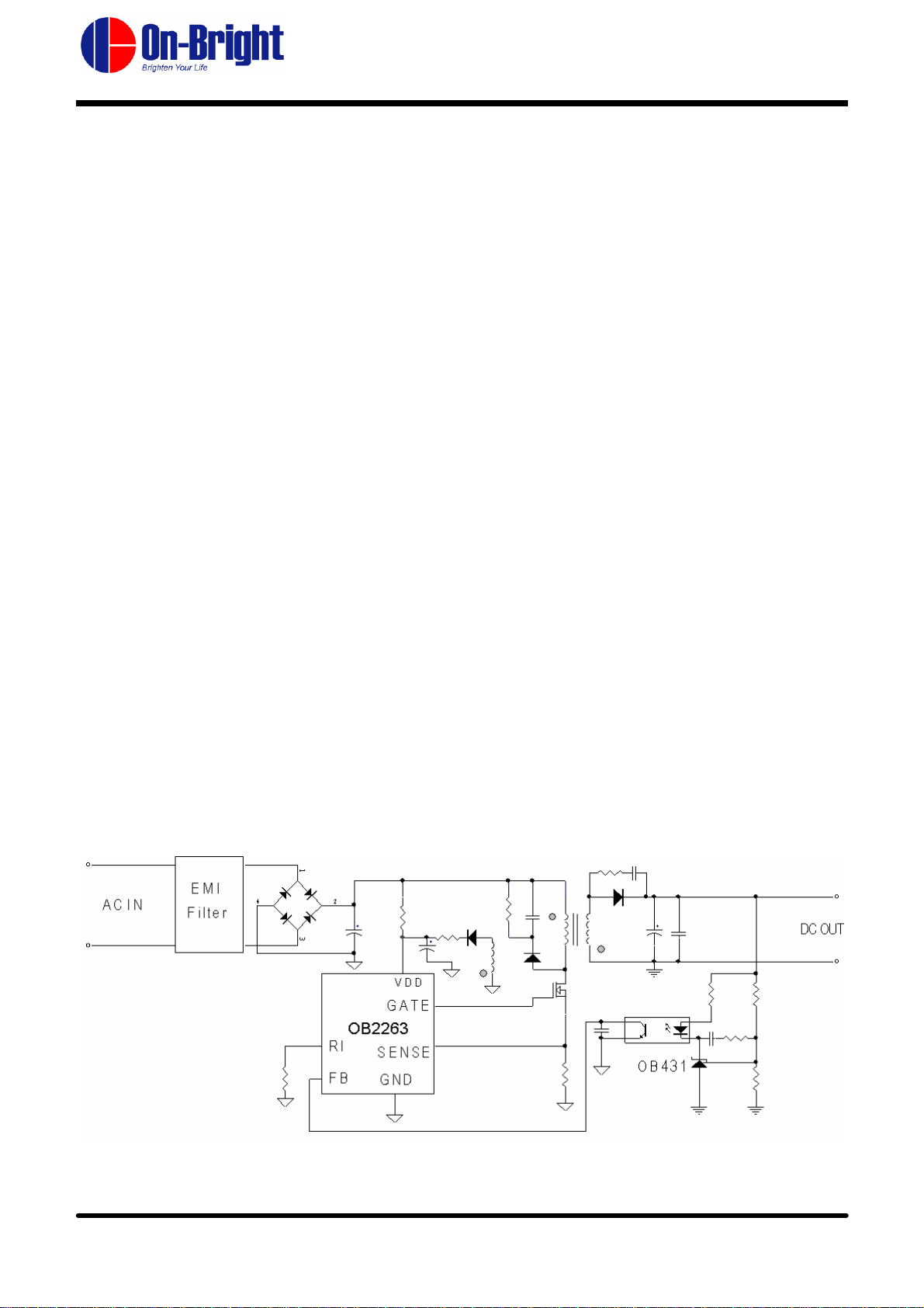
TYPICAL APPLICATION
©On-Bright Electronics
- 1 -
Confidential to Micro Bridge
OB_DOC_DS_63B5
OB2263
Current Mode PWM Controller
GENERAL INFORMATION
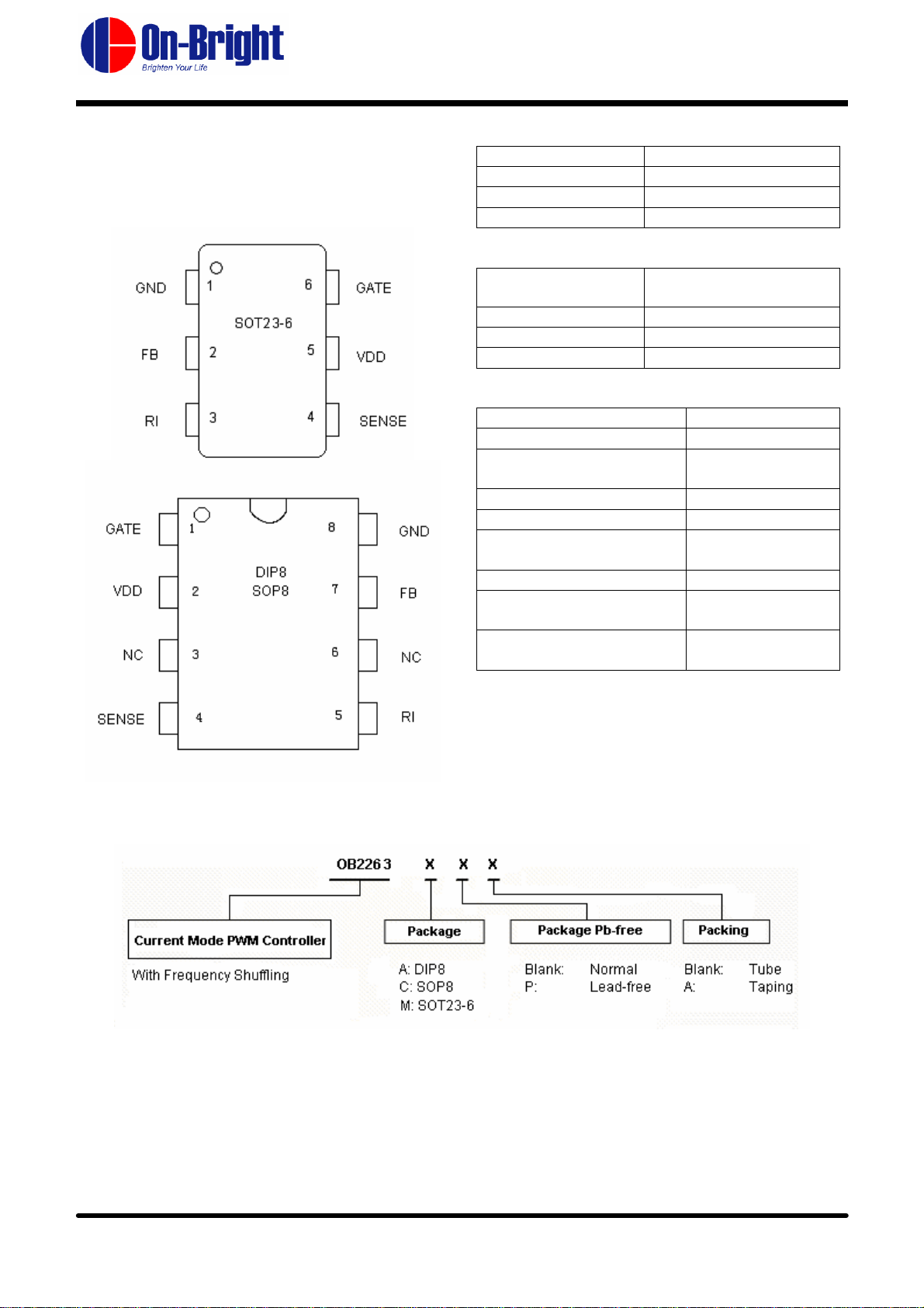
Pin Configuration
The OB2263 is offered in SOT23-6, DIP8 and SOP8
packages, shown as below.
Frequency Shuffling
Ordering Information
Part Number Description
OB2263MP SOT23-6, Pb-free
OB2263AP DIP8, Pb-free
OB2263CP SOP8, Pb-free
Package Dissipation Rating
Package
RθJA
(°C/W)
DIP8 90
SOP8 150
SOT23-6
200
Absolute Maximum Ratings
Parameter Value
VDD DC Supply Voltage 30 V
VDD Zener Clamp
Voltage
Note
VDD_Clamp+0.1V
VDD DC Clamp Current 10 mA
V
Input Voltage -0.3 to 7V
FB
V
Input Voltage to
SENSE
-0.3 to 7V
Sense Pin
VRI Input Voltage to RI Pin -0.3 to 7V
Min/Max Operating
Junction Temperature T
Min/Max Storage
Temperature T
VDD_Clamp has a nominal value of 34V.
Note:
Stresses beyond those listed under “absolute maximum ratings”
may cause permanent damage to the device. These are stress
ratings only, functional operation of the device at these or any
other conditions beyond those indicated under “recommended
operating conditions” is not implied. Exposure to absolute
maximum-rated conditions for extended periods may affect device
reliability.
stg
-20 to 150 oC
J
-55 to 160 oC
©On-Bright Electronics
- 2 -
Confidential to Micro Bridge
OB_DOC_DS_63B5
OB2263
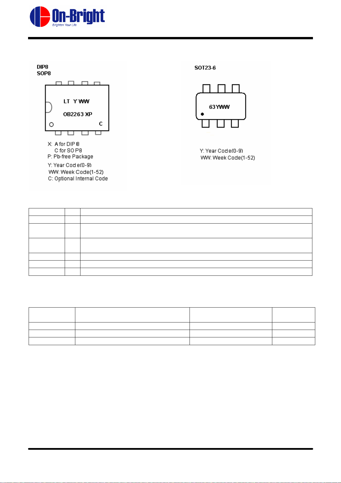
Marking Information
Current Mode PWM Controller
Frequency Shuffling
TERMINAL ASSIGNMENTS
Pin Name I/O Description
GND P Ground
FB I Feedback input pin. The PWM duty cycle is determined by voltage level into this pin and
SENSE pin input.
RI I Internal Oscillator frequency setting pin. A resistor connected between RI and GND sets
the PWM frequency.
SENSE I Current sense input pin. Connected to MOSFET current sensing resistor node.
VDD P Chip DC power supply pin.
GATE O Totem-pole gate drive output for the power MOSFET.
RECOMMENDED OPERATING CONDITION
Symbol Parameter Min
Max
VDD VDD Supply Voltage 10 to 30 V
RI RI Resistor Value 100 Kohm
T
A
Operating Ambient Temperature -20 to 85
Unit
o
C
©On-Bright Electronics
- 3 -
Confidential to Micro Bridge
OB_DOC_DS_63B5
OB2263
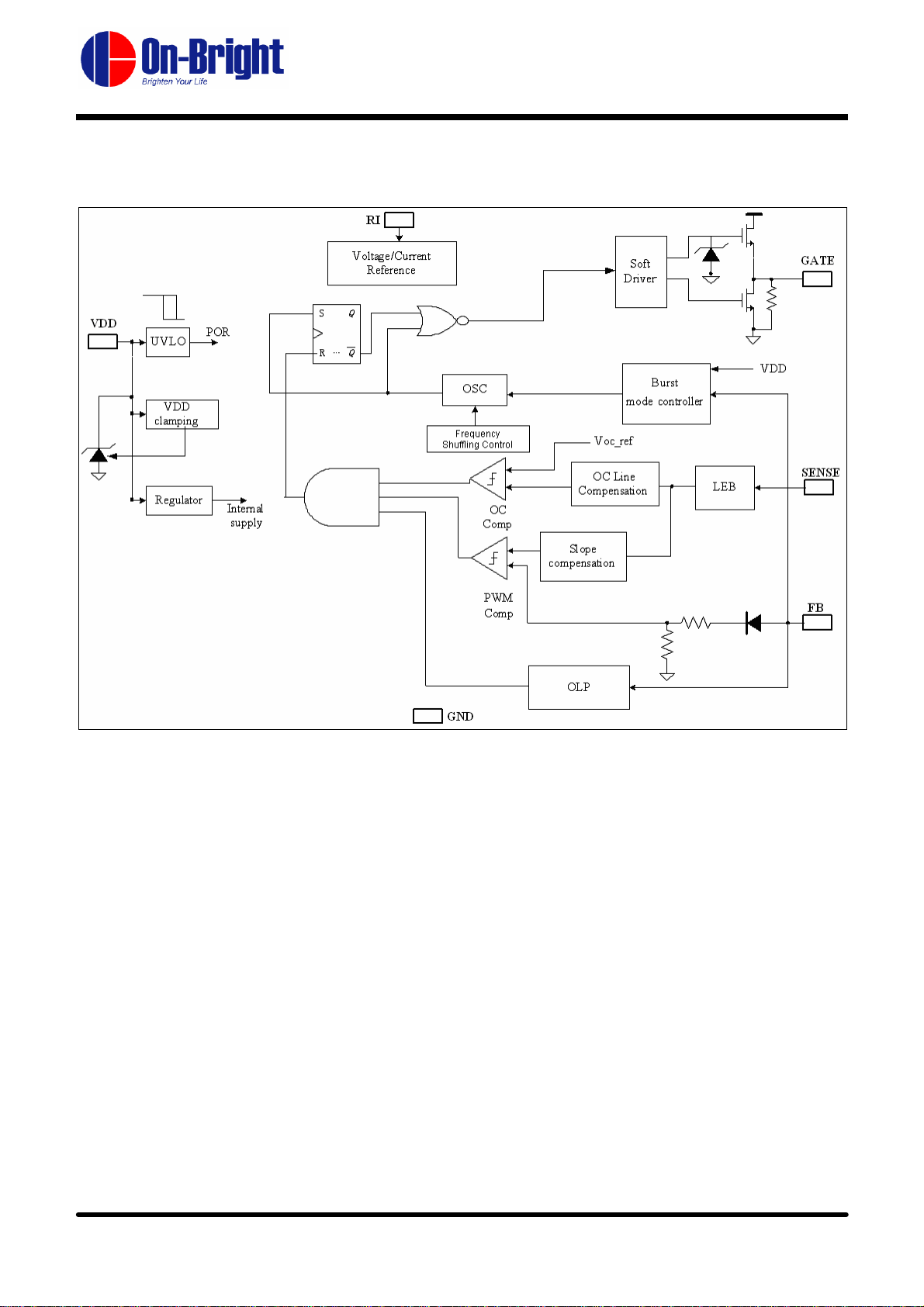
BLOCK DIAGRAM
Current Mode PWM Controller
Frequency Shuffling
©On-Bright Electronics
- 4 -
Confidential to Micro Bridge
OB_DOC_DS_63B5
 Loading...