

Page 1
SRDA05-4R2
Low Capacitance Surface
Mount TVS for High-Speed
Data Interfaces
The SRDA05-4 transient voltage suppressor is designed to protect
equipment attached to high speed communication lines from ESD,
EFT, and lightning.
http://onsemi.com
Features
•SO-8 Package
•Peak Power - 500 Watts 8 x 20 mS
•ESD Rating:
IEC 61000-4-2 (ESD) 15 kV (air) 8 kV (contact)
IEC 61000-4-4 (EFT) 40 A (5/50 ns)
IEC 61000-4-5 (lightning) 23 (8/20 ms)
•UL Flammability Rating of 94 V-0
•Pb-Free Package is Available
Typical Applications
•High Speed Communication Line Protection
MAXIMUM RATINGS
Rating Symbol Value Unit
Peak Power Dissipation
8 x 20 mS @ T
Junction and Storage Temperature Range TJ, T
Lead Solder Temperature Maximum 10 Seconds Duration
Stresses exceeding Maximum Ratings may damage the device. Maximum
Ratings are stress ratings only. Functional operation above the Recommended
Operating Conditions is not implied. Extended exposure to stresses above the
Recommended Operating Conditions may affect device reliability.
1. Non-repetitive current pulse 8 x 20 mS exponential decay waveform
= 25°C (Note 1)
A
P
pk
stg
T
L
500 W
- 55 to +150 °C
260 °C
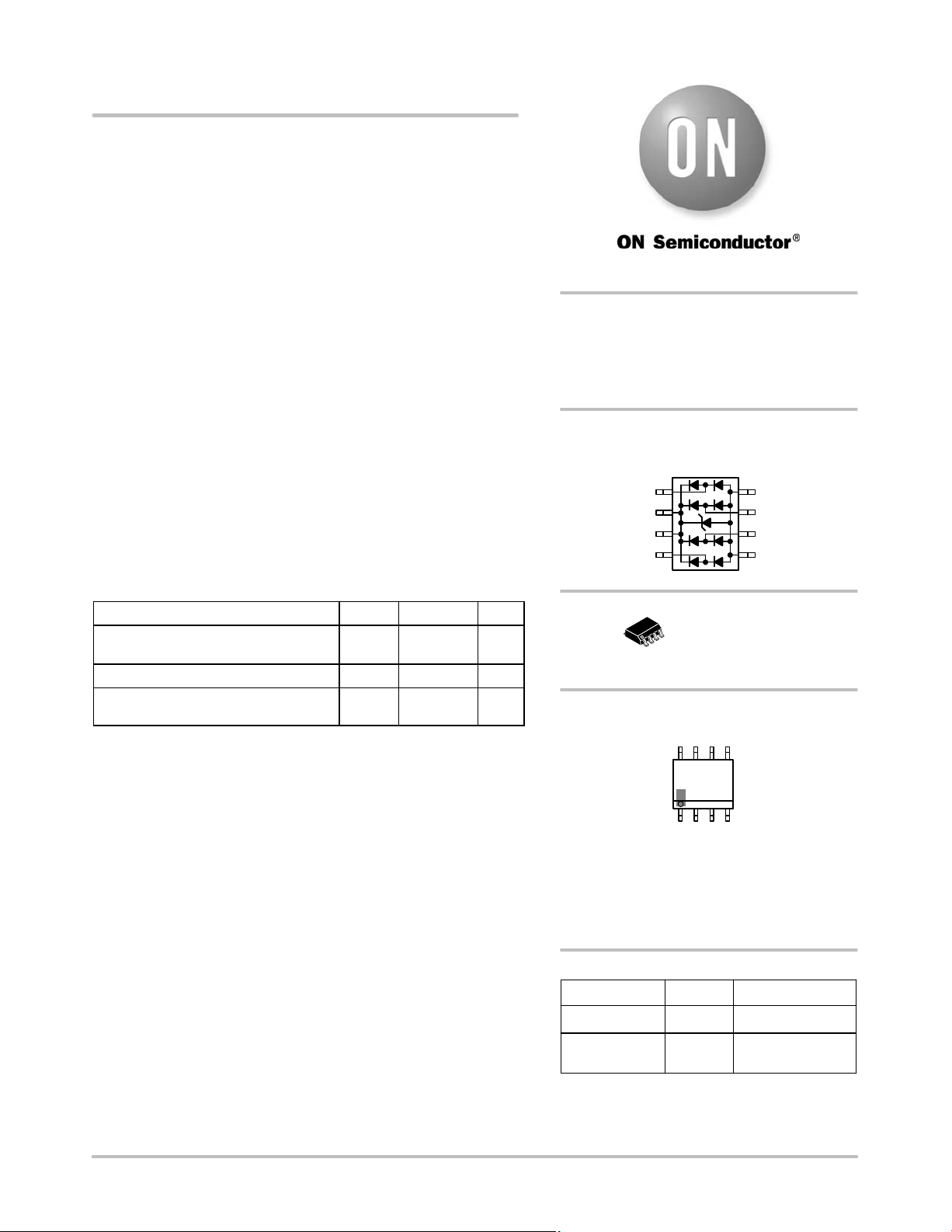
SO-8 LOW CAPACITANCE
VOLTAGE SUPPRESSOR
500 WATTS PEAK POWER
6 VOLTS
PIN CONFIGURATION
AND SCHEMATIC
I/O 1 1
REF 1 2
REF 1 3
I/O 2 4
8
1
MARKING DIAGRAM
8
SRDA5
AYWWG
G
1
8 REF 2
7 I/O 4
6 I/O 3
5 REF 2
SOIC-8
CASE 751
PLASTIC
© Semiconductor Components Industries, LLC, 2007
June, 2007 - Rev. 5
SRDA5 = Device Code
A = Assembly Location
Y = Year
WW = Work Week
G = Pb-Free Package
(Note: Microdot may be in either location)
ORDERING INFORMATION
Device Package
SRDA05-4R2 SO-8 2500/Tape & Reel
SRDA05-4R2G SO-8
(Pb-Free)
†For information on tape and reel specifications,
including part orientation and tape sizes, please
refer to our Tape and Reel Packaging Specification
Brochure, BRD8011/D.
1 Publication Order Number:
Shipping
2500/Tape & Reel
SRDA05-4R2/D
†
Page 2
SRDA05-4R2
ELECTRICAL CHARACTERISTICS
Characteristic Symbol Min Typ Max Unit
Reverse Breakdown Voltage @ It = 1.0 mA V
Reverse Leakage Current @ V
= 5.0 V I
RWN
Maximum Clamping Voltage @ IPP = 1.0 A, 8 x 20 mS
Maximum Clamping Voltage @ IPP = 10 A, 8 x 20 mS
BR
R
V
C
V
C
Between I/O Pins and Ground @ VR = 0 V, 1.0 MHz Capacitance - 10 15 pF
Between I/O Pins @ VR = 0 Volts, 1.0 MHz Capacitance - 5 8 pF
6.0 - - V
N/A - 10
N/A - 9.8 V
N/A - 12 V
mA
ELECTRICAL CHARACTERISTICS
(TA = 25°C unless otherwise noted)
UNIDIRECTIONAL (Circuit tied to Pins 1 and 3 or 2 and 3)
Symbol
I
PP
V
C
V
RWM
I
R
V
BR
I
T
QV
BR
I
F
V
F
Z
ZT
I
ZK
Z
ZK
Maximum Reverse Peak Pulse Current
Clamping Voltage @ I
Working Peak Reverse Voltage
Maximum Reverse Leakage Current @ V
Breakdown Voltage @ I
Test Current
Maximum Temperature Coefficient of V
Forward Current
Forward Voltage @ I
Maximum Zener Impedance @ I
Reverse Current
Maximum Zener Impedance @ I
Parameter
PP
RWM
T
BR
F
ZT
ZK
VCV
V
RWM
BR
Uni-Directional TVS
I
I
F
I
V
R
F
I
T
I
PP
V
http://onsemi.com
2
Page 3
SRDA05-4R2
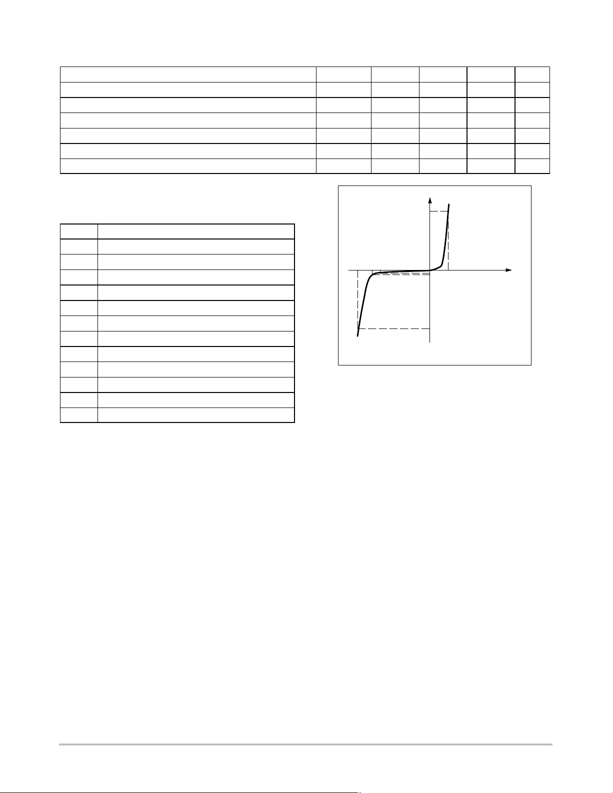
TYPICAL CHARACTERISTICS
9
8
7
6
5
4
3
2
, REVERSE BREAKDOWN (V)
Z
V
1
0
-100 0
-50
50 150
T, TEMPERATURE (°C)
100 200
Figure 1. Reverse Breakdown versus
Temperature
100
t
r
90
80
70
60
50
40
30
20
% OF PEAK PULSE CURRENT
10
0
0204060
PEAK VALUE I
t
P
@ 8 ms
RSM
PULSE WIDTH (tP) IS DEFINED
AS THAT POINT WHERE THE
PEAK CURRENT DECAY = 8 ms
HALF VALUE I
t, TIME (ms)
/2 @ 20 ms
RSM
Figure 3. 8 x 20 ms Pulse Waveform
80
8
7
6
5
4
3
2
, REVERSE LEAKAGE (mA)
R
I
1
0
-100 -50 50 100
0 150
T, TEMPERATURE (°C)
Figure 2. Reverse Leakage versus
Temperature
35
30
25
20
15
10
, CLAMPING VOLTAGE (V)
C
V
5
0
10 30 50 70 90
0204060
, PEAK PULSE CURRENT (A)
I
PP
Figure 4. Clamping Voltage versus Peak Pulse
Current
200
80
http://onsemi.com
3
Page 4

SRDA05-4R2
APPLICATIONS INFORMATION
The SRDA05-4R2 is a low capacitance TVS diode array
designed to protect sensitive electronics such as
communications systems, computers, and computer
peripherals against damage due to ESD events or transient
overvoltage conditions. Because of its low capacitance, it
can be used in high speed I/O data lines. The integrated
design of the SRDA05-4R2 offers surge rated, low
capacitance steering diodes and a TVS diode integrated in a
single package (SO-8). If a transient condition occurs, the
steering diodes will drive the transient to the positive rail of
the power supply or to ground. The TVS device protects the
power line against overvoltage conditions avoiding damage
to the power supply and other downstream components.
SRDA05-4R2 Configuration Options
The SRDA05-4R2 is able to protect up to four data lines
against transient overvoltage conditions by driving them to
a fixed reference point for clamping purposes. The steering
diodes will be forward biased whenever the voltage on the
protected line exceeds the reference voltage (Vf or Vcc+Vf).
The diodes will force the transient current to bypass the
sensitive circuit.
Data lines are connected at pins 1, 4, 6 and 7. The negative
reference is connected at pins 5 and 8. These pins must be
connected directly to ground using a ground plane to
minimize the PCB's ground inductance. It is very important
to reduce the PCB trace lengths as much as possible to
minimize parasitic inductances.
Option 1
Protection of four data lines and the power supply using
Vcc as reference.
I/O 1
I/O 2
V
CC
I/O 3
I/O 4
1
2
3
4
Figure 5.
8
7
6
5
For this configuration, connect pins 2 and 3 directly to the
positive supply rail (Vcc). The data lines are referenced to
the supply voltage. The internal TVS diode prevents
overvoltage on the supply rail. Biasing of the steering diodes
reduces their capacitance.
Option 2
Protection of four data lines with bias and power supply
isolation resistor.
I/O 1
I/O 2
V
CC
10 K
1
2
3
4
I/O 3
I/O 4
Figure 6.
8
7
6
5
The SRDA05-4R2 can be isolated from the power supply
by connecting a series resistor between pins 2 and 3 and Vcc.
A 10 kW resistor is recommended for this application. This
will maintain a bias on the internal TVS and steering diodes,
reducing their capacitance.
Option 3
Protection of four data lines using the internal TVS diode
as reference.
I/O 1
I/O 2
I/O 3
I/O 4
NC
NC
1
2
3
4
Figure 7.
8
7
6
5
In applications lacking a positive supply reference or
those cases in which a fully isolated power supply is
required, the internal TVS can be used as the reference. For
these applications, pins 2 and 3 are not connected. In this
configuration, the steering diodes will conduct whenever the
voltage on the protected line exceeds the working voltage of
the TVS plus one diode drop (Vc=Vf + V
TVS).
http://onsemi.com
4
Page 5

SRDA05-4R2
ESD Protection of Power Supply Lines
When using diodes for data line protection, referencing to
a supply rail provides advantages. Biasing the diodes reduces
their capacitance and minimizes signal distortion.
Implementing this topology with discrete devices does have
disadvantages. This configuration is shown below:
Power
Supply
Protected
Device
Data Line
V
CC
D1
D2
I
ESDpos
I
ESDneg
I
ESDpos
VF + V
CC
I
ESDneg
-VF
Figure 8.
Looking at the figure above, it can be seen that when a
positive ESD condition occurs, diode D1 will be forward
biased while diode D2 will be forward biased when a negative
ESD condition occurs. For slower transient conditions, this
system may be approximated as follows:
For positive pulse conditions:
Vc = Vcc + Vf
D1
For negative pulse conditions:
Vc = -Vf
D2
ESD events can have rise times on the order of some
number of nanoseconds. Under these conditions, the effect of
parasitic inductance must be considered. A pictorial
representation of this is shown below.
Power
Supply
V
CC
Protected
Device
D1
Data Line
D2
I
ESDpos
I
ESDpos
VC = VCC + Vf + (L diESD/dt)
I
ESDneg
I
ESDneg
L di
ESD/dt factor. A relatively small trace inductance can result
in hundreds of volts appearing on the supply rail. This
endangers both the power supply and anything attached to
that rail. This highlights the importance of good board layout.
Taking care to minimize the effects of parasitic inductance
will provide significant benefits in transient immunity.
Even with good board layout, some disadvantages are still
present when discrete diodes are used to suppress ESD events
across datalines and the supply rail. Discrete diodes with good
transient power capability will have larger die and therefore
higher capacitance. This capacitance becomes problematic as
transmission frequencies increase. Reducing capacitance
generally requires reducing die size. These small die will have
higher forward voltage characteristics at typical ESD
transient current levels. This voltage combined with the
smaller die can result in device failure.
The ON Semiconductor SRDA05- 4R2 was developed to
overcome the disadvantages encountered when using discrete
diodes for ESD protection. This device integrates a TVS
diode within a network of steering diodes.
D1
D2
Figure 10. SRDA05-4R2 Equivalent Circuit
D3
D4
D5
D6
D7
D8
0
During an ESD condition, the ESD current will be driven
to ground through the TVS diode as shown below.
Power
Supply
V
CC
I
ESDpos
D1
Protected
Device
Data Line
D2
VC = -Vf - (L diESD/dt)
Figure 9.
An approximation of the clamping voltage for these fast
transients would be:
For positive pulse conditions:
Vc = Vcc + Vf + (L di
ESD/dt)
For negative pulse conditions:
Vc = -Vf – (L di
ESD/dt)
As shown in the formulas, the clamping voltage (Vc) not
only depends on the Vf of the steering diodes but also on the
http://onsemi.com
Figure 11.
The resulting clamping voltage on the protected IC will
be:
Vc = V
FD1 + VTVS.
The clamping voltage of the TVS diode is provided in
Figure 4 and depends on the magnitude of the ESD current.
The steering diodes are fast switching devices with unique
forward voltage and low capacitance characteristics.
5
Page 6

UPSTREAM
USB PORT
V
BUS
D+
D-
GND
V
BUS
NUP2201MR6
V
BUS
SRDA05-4R2
TYPICAL APPLICATIONS
R
T
R
T
V
USB
Controller
C
C
T
T
R
T
R
T
C
C
T
T
Figure 12. ESD Protection for USB Port
BUS
SRDA05-4R2
V
BUS
V
BUS
V
BUS
D+
D-
GND
V
BUS
D+
DGND
DOWNSTREAM
USB PORT
DOWNSTREAM
USB PORT
PHY
Ethernet
(10/100)
TX+
TX-
Coupling
Transformers
RX+
RX-
SRDA05-4R2
V
CC
GND
N/C N/C
Figure 13. Protection for Ethernet 10/100 (Differential Mode)
RJ45
Connector
TX+
TX-
RX+
RX-
http://onsemi.com
6
Page 7

RTIP
RRING
T1/E1
TRANCEIVER
TTIP
SRDA05-4R2
R1
R3
R2
V
CC
SRDA05-4R2
R4
T1
TRING
R5
T2
Figure 14. TI/E1 Interface Protection
http://onsemi.com
7
Page 8

-Z-
-Y-
SRDA05-4R2
PACKAGE DIMENSIONS
SOIC-8 NB
CASE 751-07
ISSUE AH
NOTES:
-XA
58
B
1
S
0.25 (0.010)
4
M
M
Y
K
G
C
SEATING
PLANE
0.10 (0.004)
H
D
0.25 (0.010) Z
M
Y
SXS
N
X 45
_
M
J
1. DIMENSIONING AND TOLERANCING PER
ANSI Y14.5M, 1982.
2. CONTROLLING DIMENSION: MILLIMETER.
3. DIMENSION A AND B DO NOT INCLUDE
MOLD PROTRUSION.
4. MAXIMUM MOLD PROTRUSION 0.15 (0.006)
PER SIDE.
5. DIMENSION D DOES NOT INCLUDE DAMBAR
PROTRUSION. ALLOWABLE DAMBAR
PROTRUSION SHALL BE 0.127 (0.005) TOTAL
IN EXCESS OF THE D DIMENSION AT
MAXIMUM MATERIAL CONDITION.
6. 751-01 THRU 751-06 ARE OBSOLETE. NEW
STANDARD IS 751-07.
MILLIMETERS
DIMAMIN MAX MIN MAX
4.80 5.00 0.189 0.197
B 3.80 4.00 0.150 0.157
C 1.35 1.75 0.053 0.069
D 0.33 0.51 0.013 0.020
G 1.27 BSC 0.050 BSC
H 0.10 0.25 0.004 0.010
J 0.19 0.25 0.007 0.010
K 0.40 1.27 0.016 0.050
M 0 8 0 8
____
N 0.25 0.50 0.010 0.020
S 5.80 6.20 0.228 0.244
INCHES
SOLDERING FOOTPRINT*
1.52
0.060
7.0
0.275
0.6
0.024
*For additional information on our Pb-Free strategy and soldering
details, please download the ON Semiconductor Soldering and
Mounting Techniques Reference Manual, SOLDERRM/D.
ON Semiconductor and are registered trademarks of Semiconductor Components Industries, LLC (SCILLC). SCILLC reserves the right to make changes without further notice
to any products herein. SCILLC makes no warranty, representation or guarantee regarding the suitability of its products for any particular purpose, nor does SCILLC assume any liability
arising out of the application or use of any product or circuit, and specifically disclaims any and all liability, including without limitation special, consequential or incidental damages.
“Typical” parameters which may be provided in SCILLC data sheets and/or specifications can and do vary in different applications and actual performance may vary over time. All
operating parameters, including “Typicals” must be validated for each customer application by customer's technical experts. SCILLC does not convey any license under its patent rights
nor the rights of others. SCILLC products are not designed, intended, or authorized for use as components in systems intended for surgical implant into the body, or other applications
intended to support or sustain life, or for any other application in which the failure of the SCILLC product could create a situation where personal injury or death may occur. Should
Buyer purchase or use SCILLC products for any such unintended or unauthorized application, Buyer shall indemnify and hold SCILLC and its officers, employees, subsidiaries, affiliates,
and distributors harmless against all claims, costs, damages, and expenses, and reasonable attorney fees arising out of, directly or indirectly, any claim of personal injury or death
associated with such unintended or unauthorized use, even if such claim alleges that SCILLC was negligent regarding the design or manufacture of the part. SCILLC is an Equal
Opportunity/Affirmative Action Employer. This literature is subject to all applicable copyright laws and is not for resale in any manner.
4.0
0.155
1.270
0.050
SCALE 6:1
ǒ
inches
mm
Ǔ
PUBLICATION ORDERING INFORMATION
LITERATURE FULFILLMENT:
Literature Distribution Center for ON Semiconductor
P.O. Box 5163, Denver, Colorado 80217 USA
Phone: 303-675-2175 or 800-344-3860 Toll Free USA/Canada
Fax: 303-675-2176 or 800-344-3867 Toll Free USA/Canada
Email: orderlit@onsemi.com
N. American Technical Support: 800-282-9855 Toll Free
USA/Canada
Europe, Middle East and Africa Technical Support:
Phone: 421 33 790 2910
Japan Customer Focus Center
Phone: 81-3-5773-3850
http://onsemi.com
8
ON Semiconductor Website: www.onsemi.com
Order Literature: http://www.onsemi.com/orderlit
For additional information, please contact your local
Sales Representative
SRDA05-4R2/D
Page 9

 Loading...