

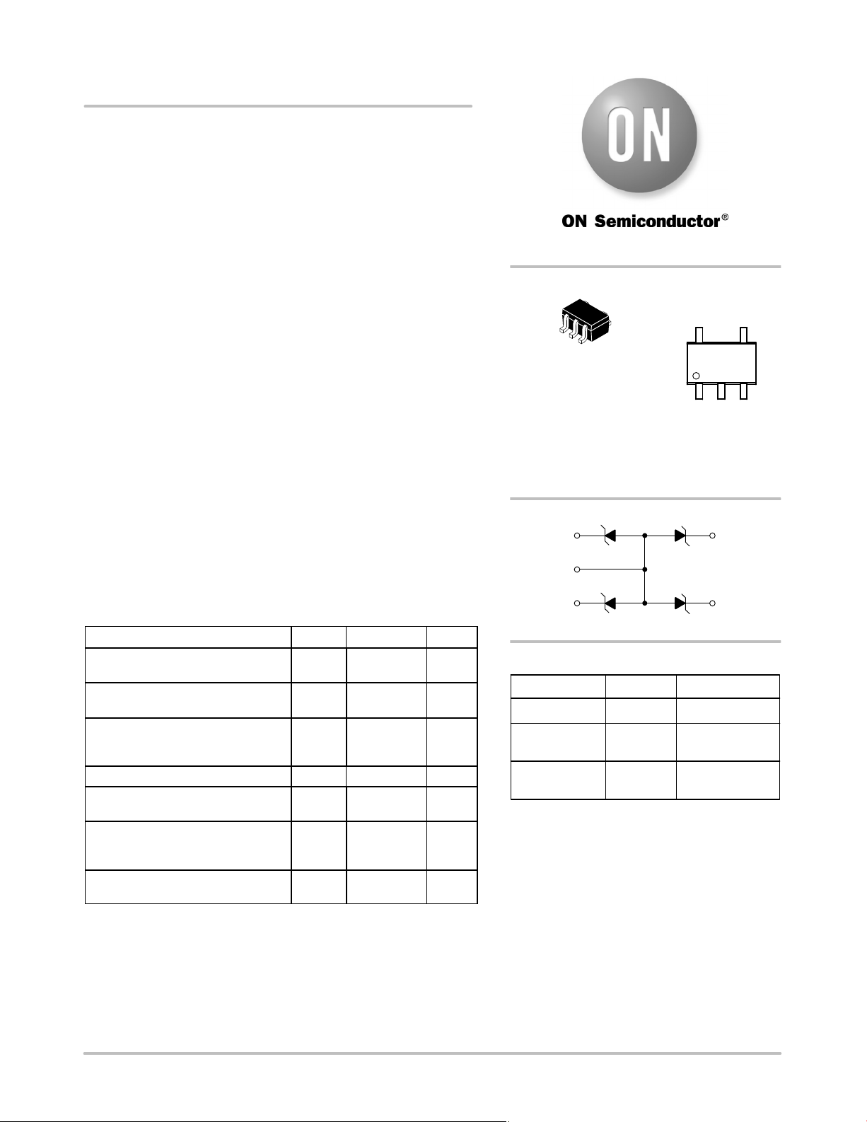
SMF05T1
Quad Array for ESD
Protection
ESD Protection Diodes with Low
Clamping Voltage
This quad monolithic silicon voltage suppressor is designed for
applications requiring transient overvoltage protection capability. It is
intended for use in voltage and ESD sensitive equipment such as
computers, printers, business machines, communication systems,
medical equipment, and other applications. Its quad junction common
anode design protects four separate lines using only one package.
These devices are ideal for situations where board space is at a
premium.
Specification Features
• Low Clamping Voltage
• Stand Off Voltage 5 V
• Low Leakage < 5 mA @ 5 V
• SC−88A Package Allows Four Separate Unidirectional
Configurations
• IEC6100−4−2 Level 4 ESD Protection
• Pb−Free Packages are Available*
Mechanical Characteristics
• Void Free, Transfer−Molded, Thermosetting Plastic Case
• Corrosion Resistant Finish, Easily Solderable
• Package Designed for Optimal Automated Board Assembly
• Small Package Size for High Density Applications
MAXIMUM RATINGS (T
Characteristic
Peak Power Dissipation @ 8 X 20 ms
@T
≤ 25°C
A
Steady State Power − 1 Diode
(Note 1)
Thermal Resistance
Junction−to−Ambient
Above 25°C, Derate
Maximum Junction Temperature T
Operating Junction and Storage
Temperature Range
ESD Discharge
IEC61000−4−2, Air Discharge
IEC61000−4−2, Contact Discharge
Lead Solder Temperature
(10 seconds duration)
Stresses exceeding Maximum Ratings may damage the device. Maximum
Ratings are stress ratings only. Functional operation above the Recommended
Operating Conditions is not implied. Extended exposure to stresses above the
Recommended Operating Conditions may affect device reliability.
1. Only 1 diode under power. For all 4 diodes under power, P
Mounted on FR−4 board with min pad.
*For additional information on our Pb−Free strategy and soldering details, please
download the ON Semiconductor Soldering and Mounting Techniques
Reference Manual, SOLDERRM/D.
See Application Note AND8308/D for further description of survivability specs.
= 25°C unless otherwise noted)
A
Symbol Value Unit
P
pk
P
D
R
q
JA
Jmax
TJ T
T
−55 to +150 °C
stg
L
200 W
385 mW
325
3.1
150 °C
30
30
260 °C
°C/W
mW/°C
kV
will be 25%.
D
Cathode
Cathode
SMF05T1 SC−88A 3000/Tape & Reel
SMF05T1G SC−88A
SMF05T2G SC−88A
†For information on tape and reel specifications,
including part orientation and tape sizes, please
refer to our Tape and Reel Packaging Specifications
Brochure, BRD8011/D.
http://onsemi.com
MARKING
DIAGRAM
45
SC−88A/SOT−323
CASE 419A
STYLE 5
60 = Device Marking
M = One Digit Date Code
G = Pb−Free Package
(Note: Microdot may be in either location)
1
2
Anode
3
60 MG
G
132
5
Cathode
4
Cathode
ORDERING INFORMATION
Device Package Shipping
(Pb−Free)
(Pb−Free)
3000/Tape & Reel
3000/Tape & Reel
†
© Semiconductor Components Industries, LLC, 2009
August, 2009 − Rev. 4
1 Publication Order Number:
SMF05T1/D
SMF05T1
ELECTRICAL CHARACTERISTICS
(TA = 25°C unless otherwise noted)
Symbol
V
I
V
RWM
V
V
P
Maximum Reverse Peak Pulse Current
PP
Clamping Voltage @ I
C
Working Peak Reverse Voltage
I
Maximum Reverse Leakage Current @ V
R
Breakdown Voltage @ I
BR
I
Test Current
T
I
Forward Current
F
Forward Voltage @ I
F
Peak Power Dissipation
pk
C Capacitance @ VR = 0 and f = 1.0 MHz
Parameter
PP
T
F
RWM
VCV
V
RWM
BR
Uni−Directional TVS
*See Application Note AND8308/D for detailed explanations of
datasheet parameters.
ELECTRICAL CHARACTERISTICS
Breakdown
Voltage
@ 1 mA
V
BR
(V)
Device
Min Max Max Max IPP (A) VC (V) IPP (A) VC (V)
SMF05 6.0 7.2 5.0 90 1.25 1.0 9.5 12 12.5 Figures 1 and 2
2. Non−repetitive current per Figure 5. Derate per Figure 6.
3. For test procedure see Figures 3 and 4 and Application Note AND8307/D.
Leakage
Current
@ V
I
R
5 V (mA)
RWM
=
Capacitance
@ 0 V Bias
(pF)
Max VF @
= 200 mA
I
F
(V)
Max Clamping
Voltage (V
@ I
(Note 2)
PP
C
)
I
I
F
I
V
R
F
I
T
I
PP
Max Clamping
Voltage (V
@ I
(Note 2)
PP
C
)
Per IEC61000−4−2
(Note 3)
See Below
V
V
C
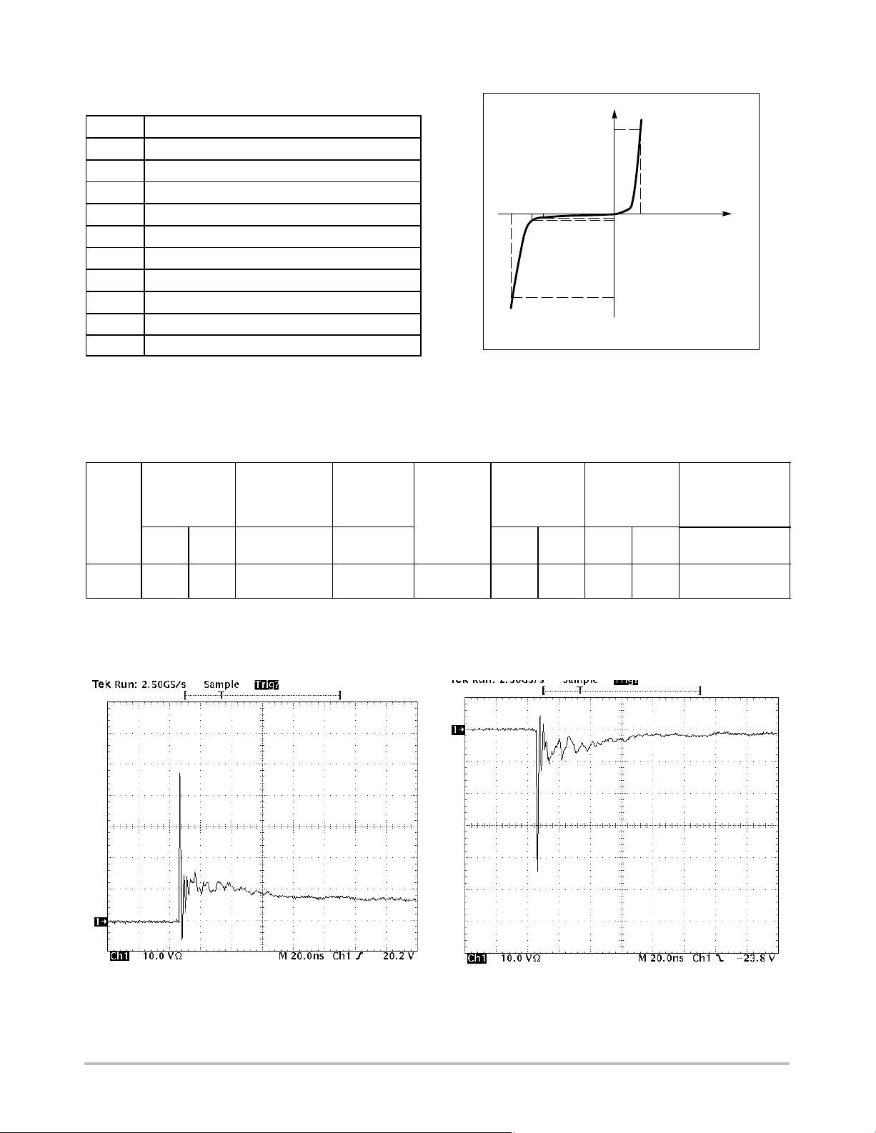
Figure 1. ESD Clamping Voltage Screenshot
Positive 8 kV Contact per IEC61000−4−2
Figure 2. ESD Clamping Voltage Screenshot
Negative 8 kV Contact per IEC61000−4−2
http://onsemi.com
2

SMF05T1
IEC 61000−4−2 Spec.
Test
Voltage
Level
1 2 7.5 4 2
2 4 15 8 4
3 6 22.5 12 6
4 8 30 16 8
(kV)
ESD Gun
First Peak
Current
(A)
Current at
30 ns (A)
TVS
50 W
Cable
IEC61000−4−2 Waveform
I
peak
Current at
60 ns (A)
100%
90%
I @ 30 ns
I @ 60 ns
10%
Figure 3. IEC61000−4−2 Spec
Oscilloscope
50 W
tP = 0.7 ns to 1 ns
Figure 4. Diagram of ESD Test Setup
The following is taken from Application Note
AND8308/D − Interpretation of Datasheet Parameters
for ESD Devices.
ESD Voltage Clamping
For sensitive circuit elements it is important to limit the
voltage that an IC will be exposed to during an ESD event
to as low a voltage as possible. The ESD clamping voltage
is the voltage drop across the ESD protection diode during
an ESD event per the IEC61000−4−2 waveform. Since the
IEC61000−4−2 was written as a pass/fail spec for larger
100
t
r
90
80
70
60
50
40
30
20
% OF PEAK PULSE CURRENT
10
0
020406080
PEAK VALUE I
t
P
Figure 5. 8 X 20 ms Pulse Waveform
systems such as cell phones or laptop computers it is not
clearly defined in the spec how to specify a clamping voltage
at the device level. ON Semiconductor has developed a way
to examine the entire voltage waveform across the ESD
protection diode over the time domain of an ESD pulse in the
form of an oscilloscope screenshot, which can be found on
the datasheets for all ESD protection diodes. For more
information on how ON Semiconductor creates these
screenshots and how to interpret them please refer to
AND8307/D.
@ 8 ms
RSM
PULSE WIDTH (tP) IS DEFINED
AS THAT POINT WHERE THE
PEAK CURRENT DECAY = 8 ms
HALF VALUE I
t, TIME (ms)
/2 @ 20 ms
RSM
http://onsemi.com
3
SMF05T1
100
90
80
C
°
70
= 25
A
60
50
40
30
OR CURRENT @ T
20
10
0
0 25 50 75 100 125 150 175 200
, AMBIENT TEMPERATURE (°C)
T
A
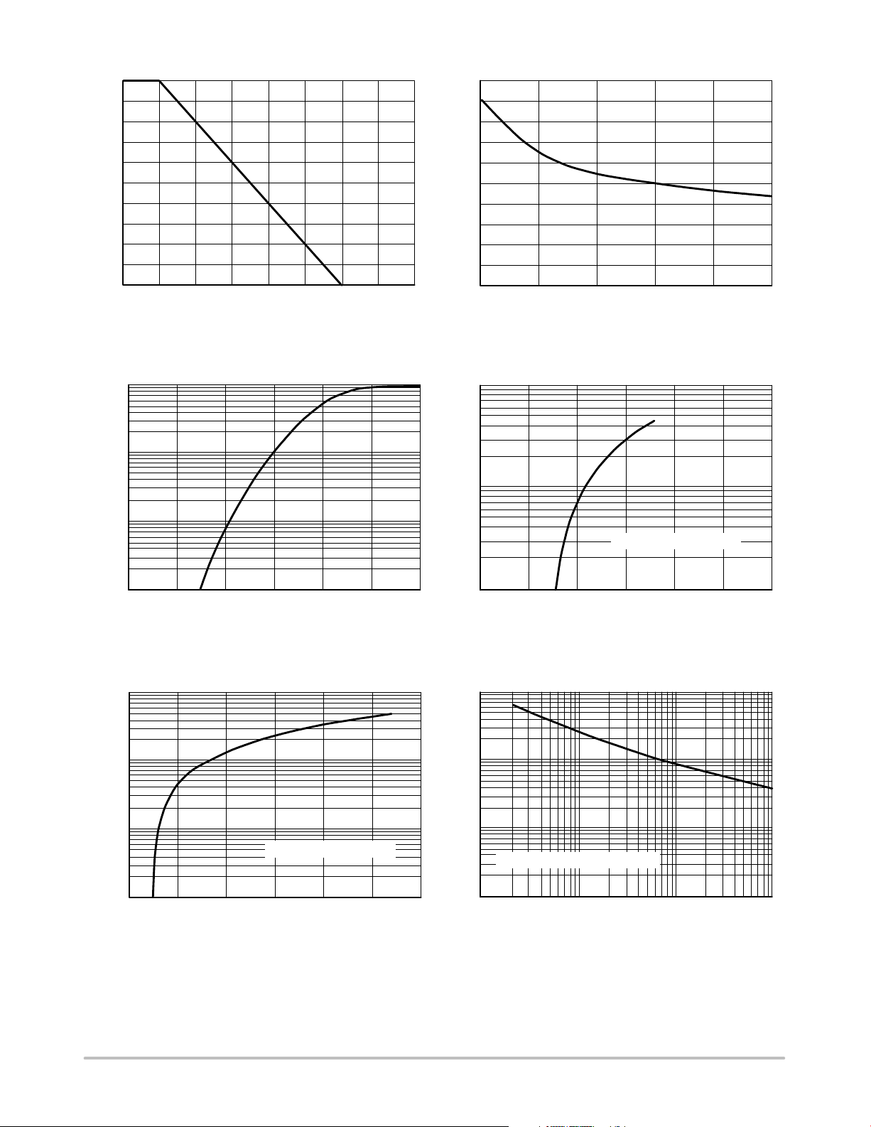
Figure 6. Pulse Derating Curve Figure 7. Capacitance
1.0
0.1
100
90
80
70
60
50
40
1 MHz FREQUENCY
30
TYPICAL CAPACITANCE (pF)
20
10
0
0 1.0 3.0 5.0
BIAS VOLTAGE (VOLTS)
100
10
4.02.0
0.01
F
I , FORWARD CURRENT (A)
0.001
0.6 0.7 0.8 0.9
V
, FORWARD VOLTAGE (VOLTS)
F
1.0 1.1 1.2
Figure 8. Forward Voltage Figure 9. Clamping Voltage versus Peak
100
10
1.0
2.5 ms SQUARE WAVE
, PEAK FORWARD PULSE CURRENT (AMPS)
pp
0.1
I
0 2.0 4.0 8.0 12
V
, FORWARD CLAMPING VOLTAGE (VOLTS)
C
6.0
Figure 10. Clamping Voltage versus Peak
Pulse Current (Forward Direction)
, PEAK PULSE CURRENT (AMPS)
pp
I
1.0
0 5.0 10 20 30
VC, CLAMPING VOLTAGE (VOLTS)
2.5 ms SQUARE WAVE
15
25
Pulse Current (Reverse Direction)
1000
100
10
, PEAK SURGE POWER (WATTS)
pk
P
10
NOTE: Non−Repetitive Surge.
1
1 10 100 1000
t, TIME (ms)
Figure 11. Pulse Width
http://onsemi.com
4

SMF05T1
PACKAGE DIMENSIONS
SC−88A/SOT−353/SC−70
5−LEAD PACKAGE
CASE 419A−02
ISSUE J
A
G
45
D
5 PL
−B−
MM
B0.2 (0.008)
S
12 3
N
J
C
H
K
NOTES:
1. DIMENSIONING AND TOLERANCING
PER ANSI Y14.5M, 1982.
2. CONTROLLING DIMENSION: INCH.
3. 419A−01 OBSOLETE. NEW STANDARD
419A−02.
4. DIMENSIONS A AND B DO NOT INCLUDE
MOLD FLASH, PROTRUSIONS, OR GATE
BURRS.
INCHES
DIMAMIN MAX MIN MAX
B 1.15 1.350.045 0.053
C 0.80 1.100.031 0.043
D 0.10 0.300.004 0.012
G 0.65 BSC0.026 BSC
H --- 0.10---0.004
J 0.10 0.250.004 0.010
K 0.10 0.300.004 0.012
N 0.20 REF0.008 REF
S 2.00 2.200.079 0.087
STYLE 5:
PIN 1. CATHODE
2. COMMON ANODE
3. CATHODE 2
4. CATHODE 3
5. CATHODE 4
MILLIMETERS
1.80 2.200.071 0.087
ON Semiconductor and are registered trademarks of Semiconductor Components Industries, LLC (SCILLC). SCILLC reserves the right to make changes without further notice
to any products herein. SCILLC makes no warranty, representation or guarantee regarding the suitability of its products for any particular purpose, nor does SCILLC assume any liability
arising out of the application or use of any product or circuit, and specifically disclaims any and all liability, including without limitation special, consequential or incidental damages.
“Typical” parameters which may be provided in SCILLC data sheets and/or specifications can and do vary in different applications and actual performance may vary over time. All
operating parameters, including “Typicals” must be validated for each customer application by customer’s technical experts. SCILLC does not convey any license under its patent rights
nor the rights of others. SCILLC products are not designed, intended, or authorized for use as components in systems intended for surgical implant into the body, or other applications
intended to support or sustain life, or for any other application in which the failure of the SCILLC product could create a situation where personal injury or death may occur. Should
Buyer purchase or use SCILLC products for any such unintended or unauthorized application, Buyer shall indemnify and hold SCILLC and its officers, employees, subsidiaries, affiliates,
and distributors harmless against all claims, costs, damages, and expenses, and reasonable attorney fees arising out of, directly or indirectly, any claim of personal injury or death
associated with such unintended or unauthorized use, even if such claim alleges that SCILLC was negligent regarding the design or manufacture of the part. SCILLC is an Equal
Opportunity/Affirmative Action Employer. This literature is subject to all applicable copyright laws and is not for resale in any manner.
PUBLICATION ORDERING INFORMATION
LITERATURE FULFILLMENT:
Literature Distribution Center for ON Semiconductor
P.O. Box 5163, Denver, Colorado 80217 USA
Phone: 303−675−2175 or 800−344−3860 Toll Free USA/Canada
Fax: 303−675−2176 or 800−344−3867 Toll Free USA/Canada
Email: orderlit@onsemi.com
N. American Technical Support: 800−282−9855 Toll Free
USA/Canada
Europe, Middle East and Africa Technical Support:
Phone: 421 33 790 2910
Japan Customer Focus Center
Phone: 81−3−5773−3850
http://onsemi.com
ON Semiconductor Website: www.onsemi.com
Order Literature: http://www.onsemi.com/orderlit
For additional information, please contact your local
Sales Representative
SMF05T1/D
5

 Loading...