

SMDA05C Series
Bi-directional TVS Array for
High-Speed Data Line
Protection
The SMDA05C transient voltage suppressor series is designed to
protect equipment attached to up to four high speed communication
lines from ESD, EFT, and lightning.
Features:
• SO−8 Package
• Peak Power − 300 W 8 x 20 mS
• ESD Rating:
IEC 61000−4−2 (ESD) ±15 kV (air) ±8 kV (contact)
IEC 61000−4−4 (EFT) 40 A (5/50 ns)
IEC 61000−4−5 (lightning) 12 A (8/20 ms)
• UL Flammability Rating of 94 V−0
• These Devices are Pb−Free, Halogen Free/BFR Free and are RoHS
Compliant
Typical Applications:
• High Speed Communication Line Protection
• Data and I/O Lines
• Microprocessor Based Equipment
• LAN/WAN Equipment
• Servers
• Notebook and Desktop PC
• Serial and Parallel Ports
• Peripherals
http://onsemi.com
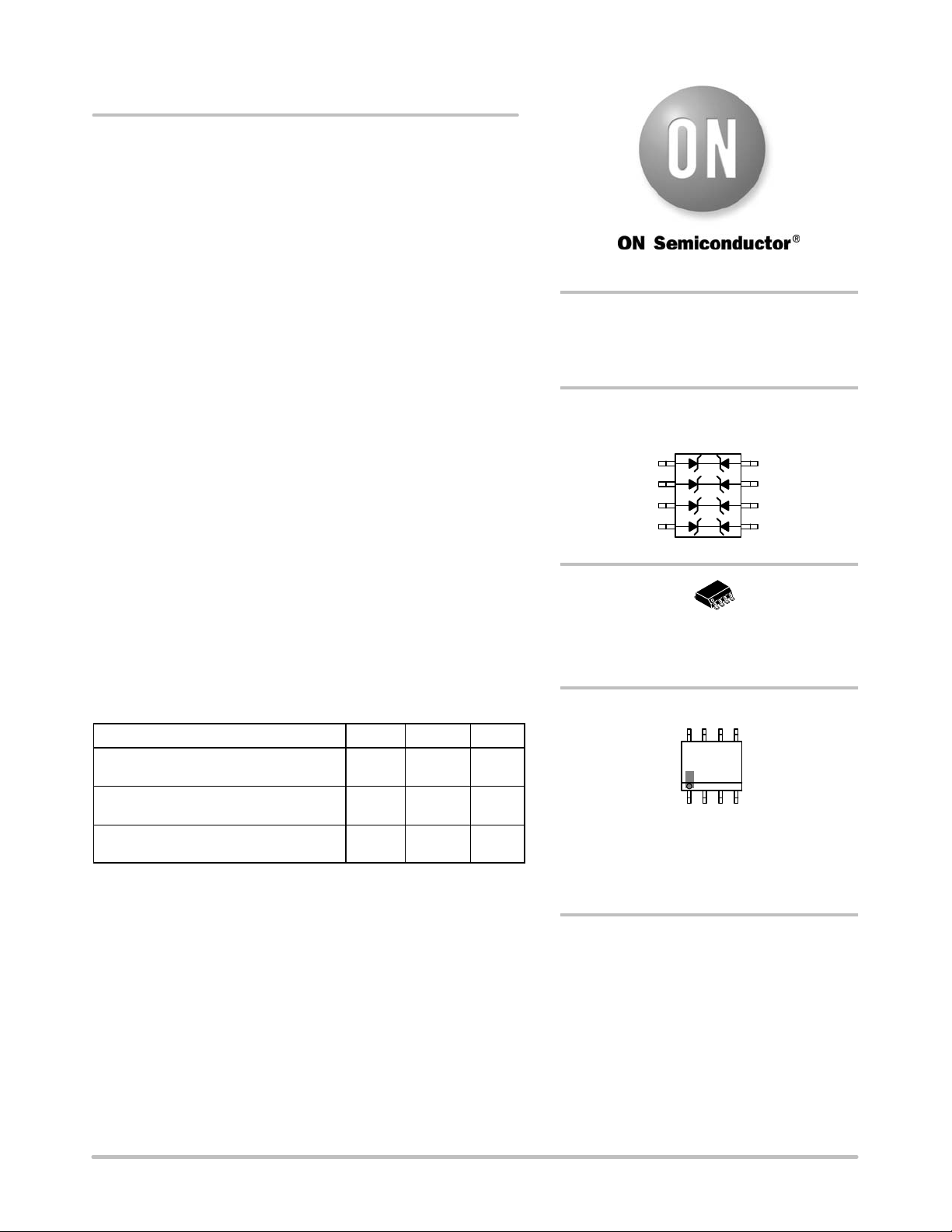
SO−8
VOLTAGE SUPPRESSOR
300 WATTS PEAK POWER
PIN CONFIGURATION
AND SCHEMATIC
1
2
3
4
8
SO−8
CASE 751
8
7
6
5
1
MAXIMUM RATINGS
Rating Symbol Value Unit
Peak Power Dissipation
8 x 20 ms @ TA = 25°C (Note 1)
Junction and Storage
Temperature Range
Lead Solder Temperature −
Maximum 10 Seconds Duration
1. Non−repetitive current pulse 8 x 20 mS exponential decay waveform
P
TJ, T
T
stg
300 W
−55 to
+150
260 °C
pk
L
°C
MARKING DIAGRAM
8
XXX
AYWWG
G
1
A = Assembly Location
Y = Year
WW = Work Week
G = Pb−Free Package
(Note: Microdot may be in either location)
ORDERING INFORMATION
See detailed ordering, marking and shipping information in the
package dimensions section on page 3 of this data sheet.
© Semiconductor Components Industries, LLC, 2011
July, 2011 − Rev. 0
1 Publication Order Number:
SMDA05C/D
SMDA05C Series
SMDA05C ELECTRICAL CHARACTERISTICS
Characteristic Symbol Min Typ Max Unit
Reverse Working Voltage V
Reverse Breakdown Voltage @ It = 1.0 mA V
Reverse Leakage Current @ V
Maximum Clamping Voltage @ IPP = 1.0 A, 8 x 20 ms
Maximum Clamping Voltage @ IPP = 5.0 A, 8 x 20 ms
Maximum Peak Pulse Current, 8 x 20 ms
Junction Capacitance @ VR = 0 V, f = 1 MHz C
SMDA12C ELECTRICAL CHARACTERISTICS
Reverse Working Voltage V
Reverse Breakdown Voltage @ It = 1.0 mA V
Reverse Leakage Current @ V
Maximum Clamping Voltage @ IPP = 1.0 A, 8 x 20 ms
Maximum Clamping Voltage @ IPP = 5.0 A, 8 x 20 ms
Maximum Peak Pulse Current, 8 x 20 ms
Junction Capacitance @ VR = 0 V, f = 1 MHz C
= 5 Volts I
RWM
Characteristic Symbol Min Typ Max Unit
= 12 Volts I
RWM
RWM
BR
R
V
C
V
C
I
PP
J
RWM
BR
R
V
C
V
C
I
PP
J
− − 5.0 V
6.0 − − V
N/A − 20
N/A − 9.8 V
N/A − 11 V
− − 17 A
− − 350 pF
− − 12 V
13.3 − − V
N/A − 1.0
N/A − 19 V
N/A − 24 V
− − 12 A
− − 120 pF
mA
mA
SMDA15C ELECTRICAL CHARACTERISTICS
Characteristic Symbol Min Typ Max Unit
Reverse Working Voltage V
Reverse Breakdown Voltage @ It = 1.0 mA V
Reverse Leakage Current @ V
= 15 Volts I
RWM
Maximum Clamping Voltage @ IPP = 1.0 A, 8 x 20 ms
Maximum Clamping Voltage @ IPP = 5.0 A, 8 x 20 ms
Maximum Peak Pulse Current, 8 x 20 ms
Junction Capacitance @ VR = 0 V, f = 1 MHz C
SMDA24C ELECTRICAL CHARACTERISTICS
Characteristic Symbol Min Typ Max Unit
Reverse Working Voltage V
Reverse Breakdown Voltage @ It = 1.0 mA V
Reverse Leakage Current @ V
Maximum Clamping Voltage @ IPP = 1.0 A, 8 x 20 ms
Maximum Clamping Voltage @ IPP = 5.0 A, 8 x 20 ms
Maximum Peak Pulse Current, 8 x 20 ms
Junction Capacitance @ VR = 0 V, f = 1 MHz C
= 24 Volts I
RWM
RWM
BR
R
V
C
V
C
I
PP
J
RWM
BR
R
V
C
V
C
I
PP
J
− − 15 V
16.7 − − V
N/A − 1.0
N/A − 24 V
N/A − 30 V
− − 10 A
− − 75 pF
− − 24 V
26.7 − − V
N/A − 1.0
N/A − 43 V
N/A − 55 V
− − 5.0 A
− − 50 pF
mA
mA
http://onsemi.com
2

SMDA05C Series
1000
100
100
90
80
70
60
50
t
r
PEAK VALUE I
RSM
@ 8 ms
PULSE WIDTH (tP) IS DEFINED
AS THAT POINT WHERE THE
PEAK CURRENT DECAY = 8 ms
HALF VALUE I
/2 @ 20 ms
RSM
40
10
NOTE: Non−Repetitive Surge.
, PEAK SURGE POWER (WATTS)
pk
P
1
1 10 100 1000
t, TIME (ms)
Figure 1. Pulse Width
30
20
10
% OF PEAK PULSE CURRENT
0
t
P
020406080
t, TIME (ms)
Figure 2. 8 × 20 ms Pulse Waveform
ORDERING INFORMATION
Device Marking Package Shipping
SMDA05CDR2G AAA SO−8
2500 / Tape & Reel
(Pb−Free)
SMDA12CDR2G AAC SO−8
2500 / Tape & Reel
(Pb−Free)
SMDA15CDR2G AAD SO−8
2500 / Tape & Reel
(Pb−Free)
SMDA24CDR2G AAE SO−8
2500 / Tape & Reel
(Pb−Free)
†For information on tape and reel specifications, including part orientation and tape sizes, please refer to our Tape and Reel Packaging
Specifications Brochure, BRD8011/D.
†
http://onsemi.com
3

−Y−
l
−Z−
SMDA05C Series
PACKAGE DIMENSIONS
SOIC−8 NB
CASE 751−07
ISSUE AK
−X−
B
H
A
58
1
4
G
D
0.25 (0.010) Z
M
S
Y
0.25 (0.010)
C
SEATING
PLANE
SXS
M
0.10 (0.004)
M
Y
K
N
X 45
_
M
J
NOTES:
1. DIMENSIONING AND TOLERANCING PER
ANSI Y14.5M, 1982.
2. CONTROLLING DIMENSION: MILLIMETER.
3. DIMENSION A AND B DO NOT INCLUDE
MOLD PROTRUSION.
4. MAXIMUM MOLD PROTRUSION 0.15 (0.006)
PER SIDE.
5. DIMENSION D DOES NOT INCLUDE DAMBAR
PROTRUSION. ALLOWABLE DAMBAR
PROTRUSION SHALL BE 0.127 (0.005) TOTAL
IN EXCESS OF THE D DIMENSION AT
MAXIMUM MATERIAL CONDITION.
6. 751−01 THRU 751−06 ARE OBSOLETE. NEW
STANDARD IS 751−07.
MILLIMETERS
DIMAMIN MAX MIN MAX
4.80 5.00 0.189 0.197
B 3.80 4.00 0.150 0.157
C 1.35 1.75 0.053 0.069
D 0.33 0.51 0.013 0.020
G 1.27 BSC 0.050 BSC
H 0.10 0.25 0.004 0.010
J 0.19 0.25 0.007 0.010
K 0.40 1.27 0.016 0.050
M 0 8 0 8
____
N 0.25 0.50 0.010 0.020
S 5.80 6.20 0.228 0.244
INCHES
SOLDERING FOOTPRINT*
1.52
0.060
7.0
0.275
0.6
0.024
*For additional information on our Pb−Free strategy and soldering
details, please download the ON Semiconductor Soldering and
Mounting Techniques Reference Manual, SOLDERRM/D.
ON Semiconductor and are registered trademarks of Semiconductor Components Industries, LLC (SCILLC). SCILLC reserves the right to make changes without further notice
to any products herein. SCILLC makes no warranty, representation or guarantee regarding the suitability of its products for any particular purpose, nor does SCILLC assume any liability
arising out of the application or use of any product or circuit, and specifically disclaims any and all liability, including without limitation special, consequential or incidental damages.
“Typical” parameters which may be provided in SCILLC data sheets and/or specifications can and do vary in different applications and actual performance may vary over time. All
operating parameters, including “Typicals” must be validated for each customer application by customer’s technical experts. SCILLC does not convey any license under its patent rights
nor the rights of others. SCILLC products are not designed, intended, or authorized for use as components in systems intended for surgical implant into the body, or other applications
intended to support or sustain life, or for any other application in which the failure of the SCILLC product could create a situation where personal injury or death may occur. Should
Buyer purchase or use SCILLC products for any such unintended or unauthorized application, Buyer shall indemnify and hold SCILLC and its officers, employees, subsidiaries, affiliates,
and distributors harmless against all claims, costs, damages, and expenses, and reasonable attorney fees arising out of, directly or indirectly, any claim of personal injury or death
associated with such unintended or unauthorized use, even if such claim alleges that SCILLC was negligent regarding the design or manufacture of the part. SCILLC is an Equal
Opportunity/Affirmative Action Employer. This literature is subject to all applicable copyright laws and is not for resale in any manner.
4.0
0.155
1.270
0.050
SCALE 6:1
ǒ
inches
mm
Ǔ
PUBLICATION ORDERING INFORMATION
LITERATURE FULFILLMENT:
Literature Distribution Center for ON Semiconductor
P.O. Box 5163, Denver, Colorado 80217 USA
Phone: 303−675−2175 or 800−344−3860 Toll Free USA/Canada
Fax: 303−675−2176 or 800−344−3867 Toll Free USA/Canada
Email: orderlit@onsemi.com
N. American Technical Support: 800−282−9855 Toll Free
USA/Canada
Europe, Middle East and Africa Technical Support:
Phone: 421 33 790 2910
Japan Customer Focus Center
Phone: 81−3−5773−3850
http://onsemi.com
4
ON Semiconductor Website: www.onsemi.com
Order Literature: http://www.onsemi.com/orderlit
For additional information, please contact your loca
Sales Representative
SMDA05C/D

 Loading...