

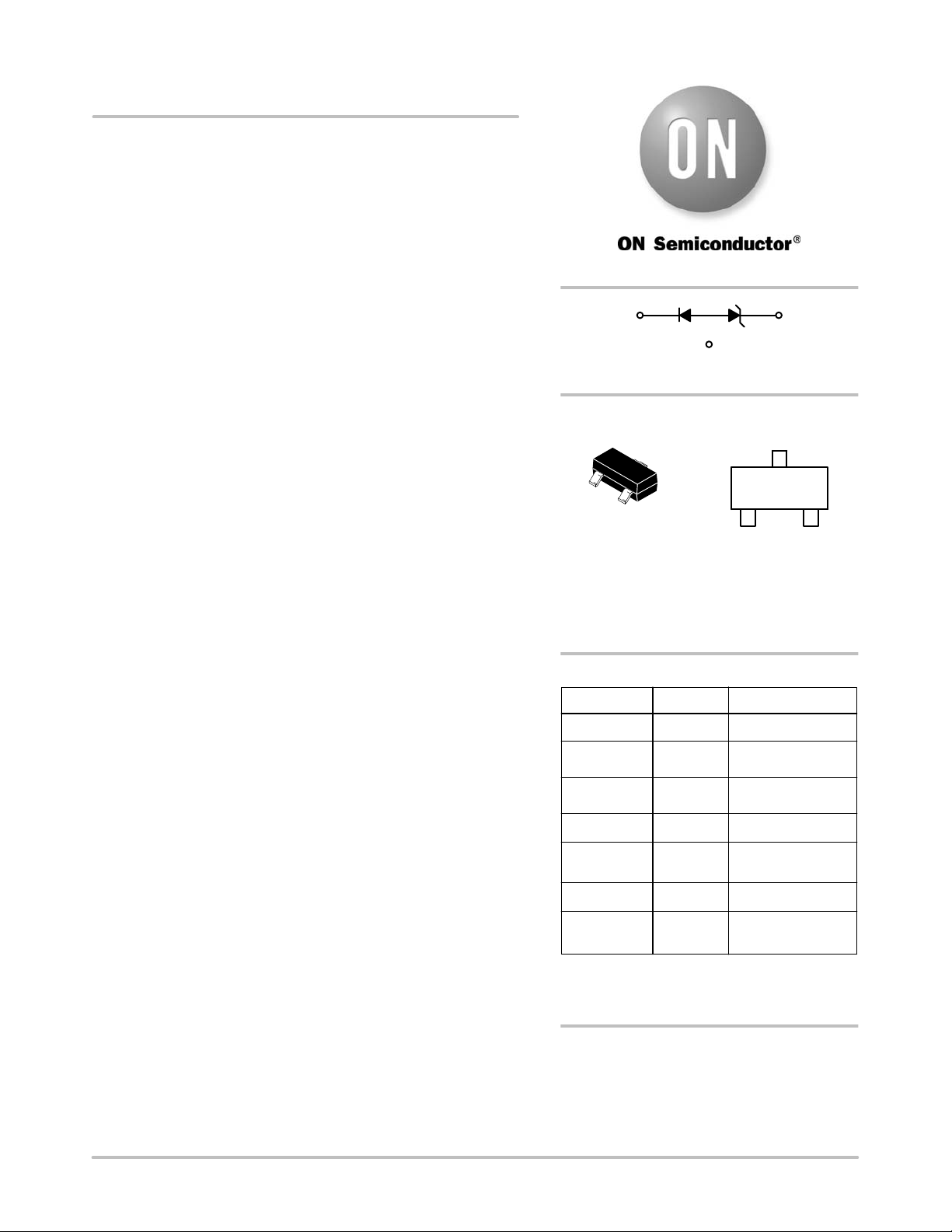
SL05T1 Series
300 Watt, SOT-23 Low
Capacitance TVS for High
Speed Line Protections
This new family of TVS offers transient overvoltage protection with
significantly reduced capacitance. The capacitance is lowered by
integrating a compensating diode in series. This integrated solution
offers ESD protection for high speed interfaces such as communication
systems, computers, and computer peripherals.
http://onsemi.com
2
1
Features
• TVS Diode in Series with a Compensating Diode Offers <5 pF
Capacitance
• ESD Protection Meeting IEC 61000−4−2, 4−4, 4−5
• Peak Power Rating of 300 W, 8 × 20 ms
• Bi−Direction Protection Can Be Achieved By Using Two Devices
• Flammability Rating UL 94 V−0
• These Devices are Pb−Free, Halogen Free/BFR Free and are RoHS
Compliant
Mechanical Characteristics:
CASE:
Void-free, transfer-molded, thermosetting plastic case
FINISH: Corrosion resistant finish, easily solderable
MAXIMUM CASE TEMPERATURE FOR SOLDERING PURPOSES:
260°C for 10 Seconds
Package designed for optimal automated board assembly
Small package size for high density applications
Available in 8 mm Tape and Reel
Use the Device Number to order the 7 inch/3,000 unit reel.
Replace the “T1” with “T3” in the Device Number to order the
13 inch/10,000 unit reel.
3
(NC)
MARKING
DIAGRAM
3
1
2
SOT−23 (TO−236)
CASE 318
STYLE 26
(Note: Microdot may be in either location)
*Date Code orientation and/or overbar may vary
depending upon manufacturing location.
ORDERING INFORMATION
Device Package Shipping
SL05T1 SOT−23 3000/Tape & Reel
SL05T1G SOT−23
SL12T1G SOT−23
SL15T1 SOT−23
SL15T1G SOT−23
SL24T1 SOT−23 3000/Tape & Reel
Lxx = Device Code
M = Date Code*
G = Pb−Free Package
(Pb−Free)
(Pb−Free)
(Pb−Free)
Lxx M G
G
xx = 05, 12, 15, or 24
†
3000/Tape & Reel
3000/Tape & Reel
3000/Tape & Reel
3000/Tape & Reel
© Semiconductor Components Industries, LLC, 2013
March, 2013 − Rev. 8
SL24T1G SOT−23
†For information on tape and reel specifications,
including part orientation and tape sizes, please
refer to our Tape and Reel Packaging Specifications
Brochure, BRD8011/D.
DEVICE MARKING INFORMATION
See specific marking information in the device marking
column of the table on page 3 of this data sheet.
1 Publication Order Number:
(Pb−Free)
3000/Tape & Reel
SL05T1/D
SL05T1 Series
MAXIMUM RATINGS
Rating Symbol Value Unit
Peak Power Dissipation @ 8x20 usec (Note 1)
≤ 25°C
@ T
L
IEC 61000−4−2 Level 4
Contact Discharge
Air Discharge
IEC 61000−4−4 EFT
IEC 61000−4−5 Lightning
Total Power Dissipation on FR−5 Board (Note 2) @ TA = 25°C
Derate above 25°C
Thermal Resistance Junction to Ambient
Total Power Dissipation on Alumina Substrate (Note 3) @ TA = 25°C
Derate above 25°C
Thermal Resistance Junction−to−Ambient
Junction and Storage Temperature Range TJ, T
Lead Solder Temperature − Maximum (10 Second Duration) T
Stresses exceeding Maximum Ratings may damage the device. Maximum Ratings are stress ratings only. Functional operation above the
Recommended Operating Conditions is not implied. Extended exposure to stresses above the Recommended Operating Conditions may affect
device reliability.
1. Non−repetitive current pulse per Figure 2
2. FR−5 = 1.0 x 0.75 x 0.62 in.
3. Alumina = 0.4 x 0.3 x 0.024 in., 99.5% alumina
P
pk
V
pp
300 W
±8
±16
40
12
°PD° 225
1.8
R
q
JA
556 °C/W
°PD° 300
2.4
R
q
JA
stg
L
417 °C/W
− 55 to +150 °C
260 °C
kV
kV
A
A
°mW°
mW/°C
°mW
mW/°C
ELECTRICAL CHARACTERISTICS
(TA = 25°C unless otherwise noted)
UNIDIRECTIONAL
Symbol Parameter
V
QV
I
PP
V
RWM
I
V
I
I
V
Z
I
ZK
Z
Maximum Reverse Peak Pulse Current
Clamping Voltage @ I
C
PP
Working Peak Reverse Voltage
Maximum Reverse Leakage Current @ V
R
Breakdown Voltage @ I
BR
Test Current
T
Maximum Temperature Coefficient of V
BR
Forward Current
F
Forward Voltage @ I
F
Maximum Zener Impedance @ I
ZT
F
Reverse Current
Maximum Zener Impedance @ I
ZK
T
ZT
ZK
BR
RWM
VCV
I
V
RWM
BR
Uni−Directional TVS
I
F
I
V
R
F
I
T
I
PP
V
http://onsemi.com
2

SL05T1 Series
ELECTRICAL CHARACTERISTICS
Breakdown Voltage
(Note 4)
VBR @ 1 mA (Volts) @ 1 A @ 5 A @ VR = 0 V, 1 MHz (pF)
Min Max (V) (V)
Device
Device
Marking
V
RWMIR
(V)
@ V
(mA)
RWM
SL05 L05 5.0 20 6.0 8.0 9.8 11 17 3.5 5.0
SL12 L12 12 1.0 13.3 15.5 19 24 12 3.5 5.0
SL15 L15 15 1.0 16.7 18.5 24 30 10 3.5 5.0
SL24 L24 24 1.0 26.7 29 43 55 5.0 3.5 5.0
4. VBR measured at pulse test current of 1 mA at an ambient temperature of 25°C
5. Surge current waveform per Figure 2
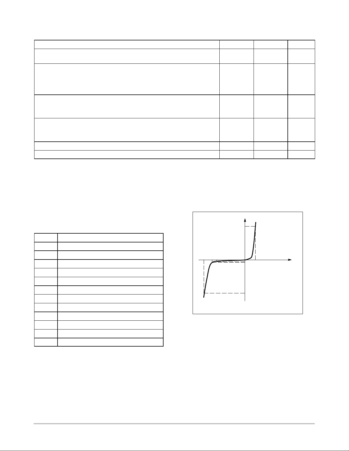
TYPICAL CHARACTERISTICS
VC, Clamping Voltage
(Note 5)
Max
I
PP
(A)
Capacitance
Typ Max
10
1
0.1
, PEAK POWER (kW)
PK
P
0.01
0.1 10
1
Figure 1. Maximum Peak Power Rating
4
3.5
3
2.5
2
1.5
1
PULSE WIDTH (ms)
100 1000
SL05
SL15
SL24
100
90
80
70
60
50
t
r
PEAK VALUE I
PULSE WIDTH (tP) IS DEFINED
AS THAT POINT WHERE THE
PEAK CURRENT DECAY = 8 ms
HALF VALUE I
RSM
@ 8 ms
RSM
/2 @ 20 ms
40
30
20
% OF PEAK PULSE CURRENT
10
0
t
P
0204060
t, TIME (ms)
Figure 2. 8 × 20 ms Pulse Waveform
10
1
0.1
LEAKAGE (mA)
80
SL05T1
0.5
C, CAPACITANCE (pF), 1 MHz FREQ.
0
@ ZERO BIAS @ V
@ 50% V
Figure 3. Typical Junction Capacitance
RWM
RWM
http://onsemi.com
3
0.01
−55 25 150
TEMPERATURE (°C)
Figure 4. Typical Leakage Over Temperature

SL05T1 Series
Applications Background
This new family of TVS devices (SL05T1 series) are
designed to protect sensitive electronics such as
communications systems, computers, and computer
peripherals against damage due to ESD conditions or
transient voltage conditions. Because of their low
capacitance value (less than 5 pF), they can be used in high
speed I/O data lines. Low capacitance is achieved by
integrating a compensating diode in series with the TVS
which is basically based in the below theoretical principle:
• Capacitance in parallel: CT = C1+C2+....+Cn
• Capacitance in series: 1/CT = (1/C1)+(1/C2)+....+(1/Cn)
The Figure 5 shows the integrated solution of the SL05T1
series device:
COMPENSATING
DIODE
Figure 5.
In the case that an over−voltage condition occurs in the I/O
line protected by the SL05T1 series device, the TVS is
reversed−biased while the compensation diode is
forward−biased so the resulting current due to the transient
voltage is drained to ground.
If protection in both polarities is required, an additional
device is connected in inverse−parallel with reference to the
first one, the Figure 6 illustrates the inverse−parallel
connection for bi−directional or unidirectional lines:
TVS
1
3
3
2
Figure 6.
2
1
An alternative solution to protect unidirectional lines, is to
connect a fast switching steering diode in parallel with the
SL05T1 series device. When the steering diode is
forward−biased, the TVS will avalanche and conduct in
reverse direction. It is important to note that by adding a
steering diode, the effective capacitance in the circuit will be
increased, therefore the impact of adding a steering diode
must be taken in consideration to establish whether the
incremental capacitance will affect the circuit functionality
or not. The Figure 7 shows the connection between the
steering diode and the SL05T1 series device:
SL05T1 DEVICE
STEERING DIODE
Figure 7.
Another typical application in which the SL05T1 series
device can be utilized, is to protect multiple I/O lines. The
protection in each of the I/O lines is achieved by connecting
two devices in inverse−parallel. The Figure 8 illustrates how
multiple I/O line protection is achieved:
OUTPUTINPUT
Figure 8.
For optimizing the protection, it is recommended to use ground planes and short path lengths to minimize the PCB’s ground inductance.
http://onsemi.com
4

A
A1
SL05T1 Series
PACKAGE DIMENSIONS
SOT−23 (TO−236)
CASE 318−08
ISSUE AP
NOTES:
1. DIMENSIONING AND TOLERANCING PER ANSI Y14.5M, 1982.
D
H
SEE VIEW C
E
c
0.25
3
E
12
b
e
q
L
L1
VIEW C
2. CONTROLLING DIMENSION: INCH.
3. MAXIMUM LEAD THICKNESS INCLUDES LEAD FINISH
THICKNESS. MINIMUM LEAD THICKNESS IS THE MINIMUM
THICKNESS OF BASE MATERIAL.
4. DIMENSIONS D AND E DO NOT INCLUDE MOLD FLASH,
PROTRUSIONS, OR GATE BURRS.
DIMAMIN NOM MAX MIN
A1 0.01 0.06 0.10 0.001
b 0.37 0.44 0.50 0.015
c 0.09 0.13 0.18 0.003
D 2.80 2.90 3.04 0.110
E 1.20 1.30 1.40 0.047
e 1.78 1.90 2.04 0.070
L 0.10 0.20 0.30 0.004
L1
H
STYLE 26:
PIN 1. CATHODE
MILLIMETERS
0.89 1.00 1.11 0.035
0.35 0.54 0.69 0.014 0.021 0.029
2.10 2.40 2.64 0.083 0.094 0.104
E
0 −−− 10 0 −−− 10q°°°°
2. ANODE
3. NO CONNECTION
INCHES
NOM MAX
0.040 0.044
0.002 0.004
0.018 0.020
0.005 0.007
0.114 0.120
0.051 0.055
0.075 0.081
0.008 0.012
SOLDERING FOOTPRINT*
0.95
0.95
0.037
0.9
0.035
0.8
0.031
*For additional information on our Pb−Free strategy and soldering
details, please download the ON Semiconductor Soldering and
Mounting Techniques Reference Manual, SOLDERRM/D.
ON Semiconductor and are registered trademarks of Semiconductor Components Industries, LLC (SCILLC). SCILLC owns the rights to a number of patents, trademarks,
copyrights, trade secrets, and other intellectual property. A listing of SCILLC’s product/patent coverage may be accessed at www.onsemi.com/site/pdf/Patent−Marking.pdf. SCILLC
reserves the right to make changes without further notice to any products herein. SCILLC makes no warranty, representation or guarantee regarding the suitability of its products for any
particular purpose, nor does SCILLC assume any liability arising out of the application or use of any product or circuit, and specifically disclaims any and all liability, including without
limitation special, consequential or incidental damages. “Typical” parameters which may be provided in SCILLC data sheets and/or specifications can and do vary in different applications
and actual performance may vary over time. All operating parameters, including “Typicals” must be validated for each customer application by customer’s technical experts. SCILLC
does not convey any license under its patent rights nor the rights of others. SCILLC products are not designed, intended, or authorized for use as components in systems intended for
surgical implant into the body, or other applications intended to support or sustain life, or for any other application in which the failure of the SCILLC product could create a situation where
personal injury or death may occur. Should Buyer purchase or use SCILLC products for any such unintended or unauthorized application, Buyer shall indemnify and hold SCILLC and
its officers, employees, subsidiaries, affiliates, and distributors harmless against all claims, costs, damages, and expenses, and reasonable attorney fees arising out of, directly or indirectly,
any claim of personal injury or death associated with such unintended or unauthorized use, even if such claim alleges that SCILLC was negligent regarding the design or manufacture
of the part. SCILLC is an Equal Opportunity/Affirmative Action Employer. This literature is subject to all applicable copyright laws and is not for resale in any manner.
0.037
SCALE 10:1
2.0
0.079
ǒ
inches
mm
Ǔ
PUBLICATION ORDERING INFORMATION
LITERATURE FULFILLMENT:
Literature Distribution Center for ON Semiconductor
P.O. Box 5163, Denver, Colorado 80217 USA
Phone: 303−675−2175 or 800−344−3860 Toll Free USA/Canada
Fax: 303−675−2176 or 800−344−3867 Toll Free USA/Canada
Email: orderlit@onsemi.com
N. American Technical Support: 800−282−9855 Toll Free
USA/Canada
Europe, Middle East and Africa Technical Support:
Phone: 421 33 790 2910
Japan Customer Focus Center
Phone: 81−3−5817−1050
http://onsemi.com
5
ON Semiconductor Website: www.onsemi.com
Order Literature: http://www.onsemi.com/orderlit
For additional information, please contact your local
Sales Representative
SL05T1/D

 Loading...