

PACDN006
6-Channel ESD Protection
Array
Product Description
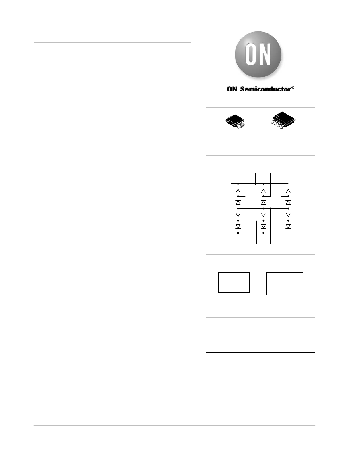
The PACDN006 is a diode array designed to provide six channels of
ESD protection for electronic components or subsystems. Each
channel consists of a pair of diodes that steer an ESD current pulse to
either the positive (V
protects against ESD pulses up to:
8 kV contact discharge, per International Standard
IEC 61000−4−2
15 kV per Human Body Model MIL−STD−883, Method 3015
(based on a 100 pF capacitor discharging through a 1.5 kW
resistor)
This device is particularly well−suited for portable electronics
(e.g., cellular phones, PDAs, notebook computers) because of its
small package footprint, high ESD protection level, and low loading
capacitance. It is also suitable for protecting video output lines and I/O
ports in computers and peripherals and is ideal for a wide range of
consumer electronics products.
The PACDN006 is available with RoHS compliant lead−free
finishing.
) or negative (VN) supply. The PACDN006
P
http://onsemi.com
MSOP 8
MR SUFFIX
CASE 846AB
ELECTRICAL SCHEMATIC
87 65
V
P
V
N
SOIC 8
SM SUFFIX
CASE 751BD
Features
Six Channels of ESD Protection
8 kV Contact, 15 kV Air ESD Protection per Channel
(IEC 61000−4−2 Standard)
15 kV of ESD Protection per Channel (HBM)
Low Loading Capacitance (3 pF Typical)
Low Leakage Current is Ideal for Battery−Powered Devices
Available in Miniature 8−Pin MSOP and 8−Pin SOIC Packages
These Devices are Pb−Free and are RoHS Compliant
Applications
Consumer Electronic Products
Cellular Phones
PDAs
Notebook Computers
Desktop PCs
Digital Cameras and Camcorders
VGA (Video) Port Protection for Desktop and Portable PCs
1 234
MARKING DIAGRAM
006R
006R = PACDN006MR
PACDN 006SM = PACDN006SM
ORDERING INFORMATION
Device Package Shipping
PACDN006MR MSOP 8
(Pb−Free)
PACDN006SM SOIC 8
(Pb−Free)
†For information on tape and reel specifications,
including part orientation and tape sizes, please
refer to our Tape and Reel Packaging Specification
Brochure, BRD8011/D.
PACDN 006SM
†
4000/Tape & Reel
2500/Tape & Reel
Semiconductor Components Industries, LLC, 2011
October, 2011 − Rev. 5
1 Publication Order Number:
PACDN006/D
PACDN006
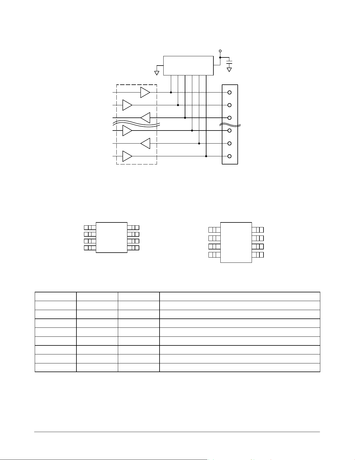
TYPICAL APPLICATION CIRCUIT
V
CC
CH1
CH2
V
CH3
N
I/O Port
Buffers
* Decoupling capacitor must be placed as close as possible to Pin7.
Top View
1
27
006R
8
36
4
5
8−Pin MSOP−8
37
PACDN006
2 4 5 6 81
Handheld/PDA ESD Protection
PACKAGE / PINOUT DIAGRAMS
CH6
V
P
CH5
CH4
CH1
CH2
V
CH3
N
0.22 mF*
Expansion
Connector
Top View
PACDN 006SM
1
8
27
36
4
5
CH6
V
P
CH5
CH4
8−Pin SOIC−8
Table 1. PIN DESCRIPTIONS
Pin Name Type Description
1 CH1 I/O ESD Channel
2 CH2 I/O ESD Channel
3 V
N
4 CH3 I/O ESD Channel
5 CH4 I/O ESD Channel
6 CH5 I/O ESD Channel
7 V
P
8 CH6 I/O ESD Channel
GND Negative Voltage Supply Rail or Ground Reference Rail
Supply Positive Voltage Supply Rail
http://onsemi.com
2
PACDN006
SPECIFICATIONS
Table 2. ABSOLUTE MAXIMUM RATINGS
Parameter Rating Units
Supply Voltage (VP − VN) 6.0 V
Diode Forward DC Current (Note 1) 20 mA
Operating Temperature Range −40 to +85 C
Storage Temperature Range −65 to +150 C
DC Voltage at any Channel Input (VN − 0.5) to (VP + 0.5) V
Package Power Rating 200 mW
Stresses exceeding Maximum Ratings may damage the device. Maximum Ratings are stress ratings only. Functional operation above the
Recommended Operating Conditions is not implied. Extended exposure to stresses above the Recommended Operating Conditions may affect
device reliability.
1. Only one diode conducting at a time.
Table 3. STANDARD OPERATING CONDITIONS
Parameter Rating Units
Operating Temperature Range −40 to +85 C
Operating Supply Voltage (VP − VN) 0 to 5.5 V
Table 4. ELECTRICAL OPERATING CHARACTERISTICS (Note 1)
Symbol
I
V
I
LEAK
C
V
ESD
P
Supply Current (VP − VN) = 5.5 V 10
Diode Forward Voltage I
F
Channel Leakage Current 0.1 1.0
Channel Input Capacitance @ 1 MHz, VP = 5 V,
IN
ESD Protection
Peak Discharge Voltage at any
Channel Input, in System
a) Human Body Model,
MIL−STD−883, Method 3015
b) Contact Discharge per
IEC 61000−4−2
c) Air Discharge per IEC 61000−4−2
V
CL
Channel Clamp Voltage
Positive Transients
Negative Transients
1. All parameters specified at TA = 25C unless otherwise noted. VP = 5 V, VN = 0 V unless noted.
2. From I/O pins to V
3. Human Body Model per MIL−STD−883, Method 3015, C
4. Standard IEC 61000−4−2 with C
Parameter Conditions Min Typ Max Units
= 20 mA 0.65 0.95 V
F
V
= 0 V, VIN = 2.5 V
N
(Note 2)
(Note 3)
(Note 4)
(Note 4)
15
8
15
@ 15 kV ESD HBM
or VN only. VP bypassed to VN with a 0.22 mF ceramic capacitor (see Application Information for more details).
P
= 150 pF, R
Discharge
Discharge
= 100 pF, R
Discharge
= 330 W, VP = 5.0 V, VN grounded.
Discharge
= 1.5 kWVP = 5.0 V, V
mA
mA
3 5 pF
kV
VP + 13.0
VN − 13.0
grounded.
N
V
http://onsemi.com
3

Input Capacitance vs. Input Voltage
PACDN006
PERFORMANCE INFORMATION
Figure 1. Typical Variation of CIN vs. V
(VP = 5 V, VN = 0 V, 0.1 mF Chip Capacitor between VP and VN)
IN
APPLICATION INFORMATION
Design Considerations
In order to realize the maximum protection against ESD pulses, care must be taken in the PCB layout to minimize parasitic
series inductances on the Supply/Ground rails as well as the signal trace segment between the signal input (typically
a connector) and the ESD protection device. Refer to Figure 2, which illustrates an example of a positive ESD pulse striking
an input channel. The parasitic series inductance back to the power supply is represented by L
and L2. The voltage VCL on
1
the line being protected is:
where I
+ FwdVoltageDropofD1) V
V
CL
is the ESD current pulse, and V
ESD
is the positive supply voltage.
SUPPLY
SUPPLY
) L1 d(I
)ńdt ) L2 d(I
ESD
ESD
)ńdt
An ESD current pulse can rise from zero to its peak value in a very short time. As an example, a level 4 contact discharge
per the IEC61000−4−2 standard results in a current pulse that rises from zero to 30 Amps in 1 ns. Here d(I
approximated by DI
increment in V
CL
/Dt, or 30/(1x10−9). So just 10 nH of series inductance (L
ESD
!
Similarly for negative ESD pulses, parasitic series inductance from the V
1
pin to the ground rail will lead to drastically
N
and L
combined) will lead to a 300 V
2
)/dt can be
ESD
increased negative voltage on the line being protected.
Another consideration is the output impedance of the power supply for fast transient currents. Most power supplies exhibit
a much higher output impedance to fast transient current spikes. In the V
given by (V
of the power supply respectively. As an example, a R
DC
+ I
ESD
x R
), where VDC and R
OUT
are the nominal supply DC output voltage and effective output impedance
OUT
of 1 W would result in a 10 V increment in VCL for a peak I
OUT
equation above, the V
CL
term, in reality, is
SUPPLY
ESD
of
10 A.
If the inductances and resistance described above are close to zero, the rail−clamp ESD protection diodes will do a good job
of protection. However, since this is not possible in practical situations, a bypass capacitor must be used to absorb the very high
frequency ESD energy. So for any brand of rail−clamp ESD protection diodes, a bypass capacitor should be connected between
the V
pin of the diodes and the ground plane (VN pin of the diodes) as shown in the Application Circuit diagram below. A value
P
of 0.22 mF is adequate for IEC−61000−4−2 level 4 contact discharge protection (8 kV). Ceramic chip capacitors mounted with
short printed circuit board traces are good choices for this application. Electrolytic capacitors should be avoided as they have
poor high frequency characteristics. For extra protection, connect a zener diode in parallel with the bypass capacitor to mitigate
http://onsemi.com
4

PACDN006
the effects of the parasitic series inductance inherent in the capacitor. The breakdown voltage of the zener diode should be
slightly higher than the maximum supply voltage.
As a general rule, the ESD Protection Array should be located as close as possible to the point of entry of expected
electrostatic discharges. The power supply bypass capacitor mentioned above should be as close to the V
Array as possible, with minimum PCB trace lengths to the power supply, ground planes and between the signal input and the
ESD device to minimize stray series inductance.
Additional Information
See also ON Semiconductor Application Notes AP209, “Design Considerations for ESD Protection” and AP219, “ESD
Protection for USB 2.0 Systems”.
L
2
V
P
PATH OF ESD CURRENT PULSE I
POSITIVE SUPPLY RAIL
ESD
pin of the Protection
P
0.22 mF
V
N
D
1
ONE
CHANNEL
D
2
OF
PACDN006
L
1
CHANNEL
INPUT
0 A
20 A
LINE BEING
PROTECTED
V
CL
GROUND RAIL
SYSTEM OR
CIRCUITRY
BEING
PROTECTED
CHASSIS GROUND
Figure 2. Application of Positive ESD Pulse between Input Channel and Ground
http://onsemi.com
5

PACDN006
PACKAGE DIMENSIONS
MSOP8
CASE 846AB−01
ISSUE O
SEATING
PLANE
−T−
0.038 (0.0015)
PIN 1 ID
8X
0.041
DD
H
E
e
E
b
A
A1
SOLDERING FOOTPRINT*
1.04
0.38
0.015
8 PL
M
0.08 (0.003) A
B
T
c
8X
NOTES:
1. DIMENSIONING AND TOLERANCING PER ANSI Y14.5M, 1982.
2. CONTROLLING DIMENSION: MILLIMETER.
3. DIMENSION A DOES NOT INCLUDE MOLD FLASH, PROTRUSIONS OR GATE
BURRS. MOLD FLASH, PROTRUSIONS OR GATE BURRS SHALL NOT EXCEED
0.15 (0.006) PER SIDE.
4. DIMENSION B DOES NOT INCLUDE INTERLEAD FLASH OR PROTRUSION.
INTERLEAD FLASH OR PROTRUSION SHALL NOT EXCEED 0.25 (0.010) PER SIDE.
5. 846A-01 OBSOLETE, NEW STANDARD 846A-02.
DIMAMIN NOM MAX MIN
S
S
A1 0.05 0.08 0.15 0.002
b 0.25 0.33 0.40 0.010
c 0.13 0.18 0.23 0.005
D 2.90 3.00 3.10 0.114
E 2.90 3.00 3.10 0.114
e 0.65 BSC
L 0.40 0.55 0.70 0.016
H
E
MILLIMETERS
−− −− 1.10 −−
4.75 4.90 5.05 0.187 0.193 0.199
INCHES
NOM MAX
−− 0.043
0.003 0.006
0.013 0.016
0.007 0.009
0.118 0.122
0.118 0.122
0.026 BSC
0.021 0.028
L
6X
0.0256
3.20
0.126
0.65
0.167
4.24
SCALE 8:1
5.28
0.208
ǒ
inches
mm
Ǔ
*For additional information on our Pb−Free strategy and soldering
details, please download the ON Semiconductor Soldering and
Mounting Techniques Reference Manual, SOLDERRM/D.
http://onsemi.com
6

PIN # 1
IDENTIFICATION
PACDN006
PACKAGE DIMENSIONS
SOIC 8, 150 mils
CASE 751BD−01
ISSUE O
E1 E
SYMBOL MIN NOM MAX
A1
E1
A
1.35
0.10
b
c
D
E
0.33
0.19
4.80
5.80
3.80
e
h
L
θ
0.25
0.40 1.27
0º 8º
1.27 BSC
1.75
0.25
0.51
0.25
5.00
6.20
4.00
0.50
TOP VIEW
D
A1
A
θ
h
c
e
SIDE VIEW
b
L
END VIEW
Notes:
(1) All dimensions are in millimeters. Angles in degrees.
(2) Complies with JEDEC MS-012.
ON Semiconductor and are registered trademarks of Semiconductor Components Industries, LLC (SCILLC). SCILLC reserves the right to make changes without further notice
to any products herein. SCILLC makes no warranty, representation or guarantee regarding the suitability of its products for any particular purpose, nor does SCILLC assume any liability
arising out of the application or use of any product or circuit, and specifically disclaims any and all liability, including without limitation special, consequential or incidental damages.
“Typical” parameters which may be provided in SCILLC data sheets and/or specifications can and do vary in different applications and actual performance may vary over time. All
operating parameters, including “Typicals” must be validated for each customer application by customer’s technical experts. SCILLC does not convey any license under its patent rights
nor the rights of others. SCILLC products are not designed, intended, or authorized for use as components in systems intended for surgical implant into the body, or other applications
intended to support or sustain life, or for any other application in which the failure of the SCILLC product could create a situation where personal injury or death may occur. Should
Buyer purchase or use SCILLC products for any such unintended or unauthorized application, Buyer shall indemnify and hold SCILLC and its officers, employees, subsidiaries, affiliates,
and distributors harmless against all claims, costs, damages, and expenses, and reasonable attorney fees arising out of, directly or indirectly, any claim of personal injury or death
associated with such unintended or unauthorized use, even if such claim alleges that SCILLC was negligent regarding the design or manufacture of the part. SCILLC is an Equal
Opportunity/Affirmative Action Employer. This literature is subject to all applicable copyright laws and is not for resale in any manner.
PUBLICATION ORDERING INFORMATION
LITERATURE FULFILLMENT:
Literature Distribution Center for ON Semiconductor
P.O. Box 5163, Denver, Colorado 80217 USA
Phone: 303−675−2175 or 800−344−3860 Toll Free USA/Canada
Fax: 303−675−2176 or 800−344−3867 Toll Free USA/Canada
Email: orderlit@onsemi.com
N. American Technical Support: 800−282−9855 Toll Free
USA/Canada
Europe, Middle East and Africa Technical Support:
Phone: 421 33 790 2910
Japan Customer Focus Center
Phone: 81−3−5817−1050
http://onsemi.com
7
ON Semiconductor Website: www.onsemi.com
Order Literature: http://www.onsemi.com/orderlit
For additional information, please contact your local
Sales Representative
PACDN006/D

 Loading...