PACDN006
6-Channel ESD Protection
Array
Product Description
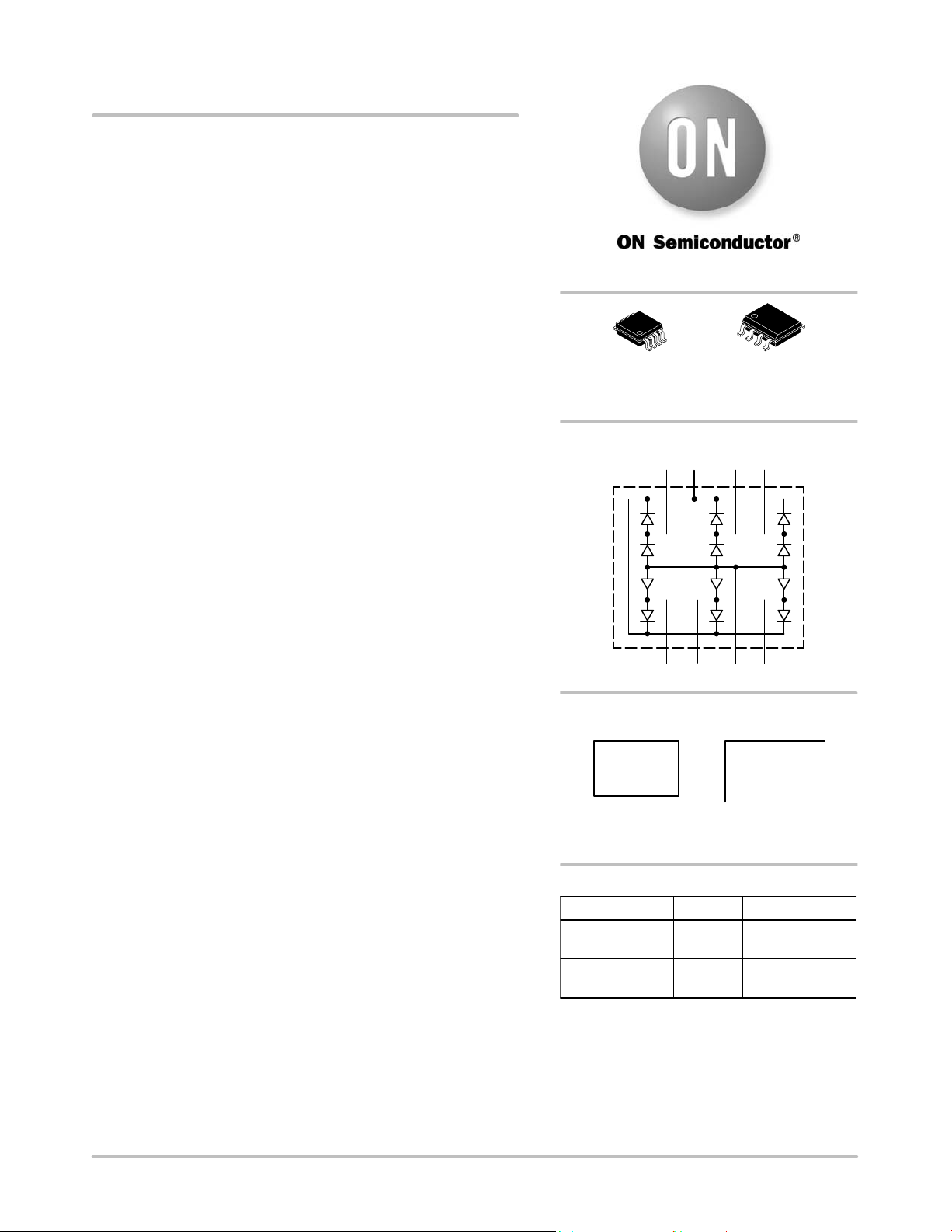
The PACDN006 is a diode array designed to provide six channels of
ESD protection for electronic components or subsystems. Each
channel consists of a pair of diodes that steer an ESD current pulse to
either the positive (V
protects against ESD pulses up to:
8 kV contact discharge, per International Standard
IEC 61000−4−2
15 kV per Human Body Model MIL−STD−883, Method 3015
(based on a 100 pF capacitor discharging through a 1.5 kW
resistor)
This device is particularly well−suited for portable electronics
(e.g., cellular phones, PDAs, notebook computers) because of its
small package footprint, high ESD protection level, and low loading
capacitance. It is also suitable for protecting video output lines and I/O
ports in computers and peripherals and is ideal for a wide range of
consumer electronics products.
The PACDN006 is available with RoHS compliant lead−free
finishing.
) or negative (VN) supply. The PACDN006
P
http://onsemi.com
MSOP 8
MR SUFFIX
CASE 846AB
ELECTRICAL SCHEMATIC
87 65
V
P
V
N
SOIC 8
SM SUFFIX
CASE 751BD
Features
Six Channels of ESD Protection
8 kV Contact, 15 kV Air ESD Protection per Channel
(IEC 61000−4−2 Standard)
15 kV of ESD Protection per Channel (HBM)
Low Loading Capacitance (3 pF Typical)
Low Leakage Current is Ideal for Battery−Powered Devices
Available in Miniature 8−Pin MSOP and 8−Pin SOIC Packages
These Devices are Pb−Free and are RoHS Compliant
Applications
Consumer Electronic Products
Cellular Phones
PDAs
Notebook Computers
Desktop PCs
Digital Cameras and Camcorders
VGA (Video) Port Protection for Desktop and Portable PCs
1 234
MARKING DIAGRAM
006R
006R = PACDN006MR
PACDN 006SM = PACDN006SM
ORDERING INFORMATION
Device Package Shipping
PACDN006MR MSOP 8
(Pb−Free)
PACDN006SM SOIC 8
(Pb−Free)
†For information on tape and reel specifications,
including part orientation and tape sizes, please
refer to our Tape and Reel Packaging Specification
Brochure, BRD8011/D.
PACDN 006SM
†
4000/Tape & Reel
2500/Tape & Reel
Semiconductor Components Industries, LLC, 2011
October, 2011 − Rev. 5
1 Publication Order Number:
PACDN006/D

PACDN006
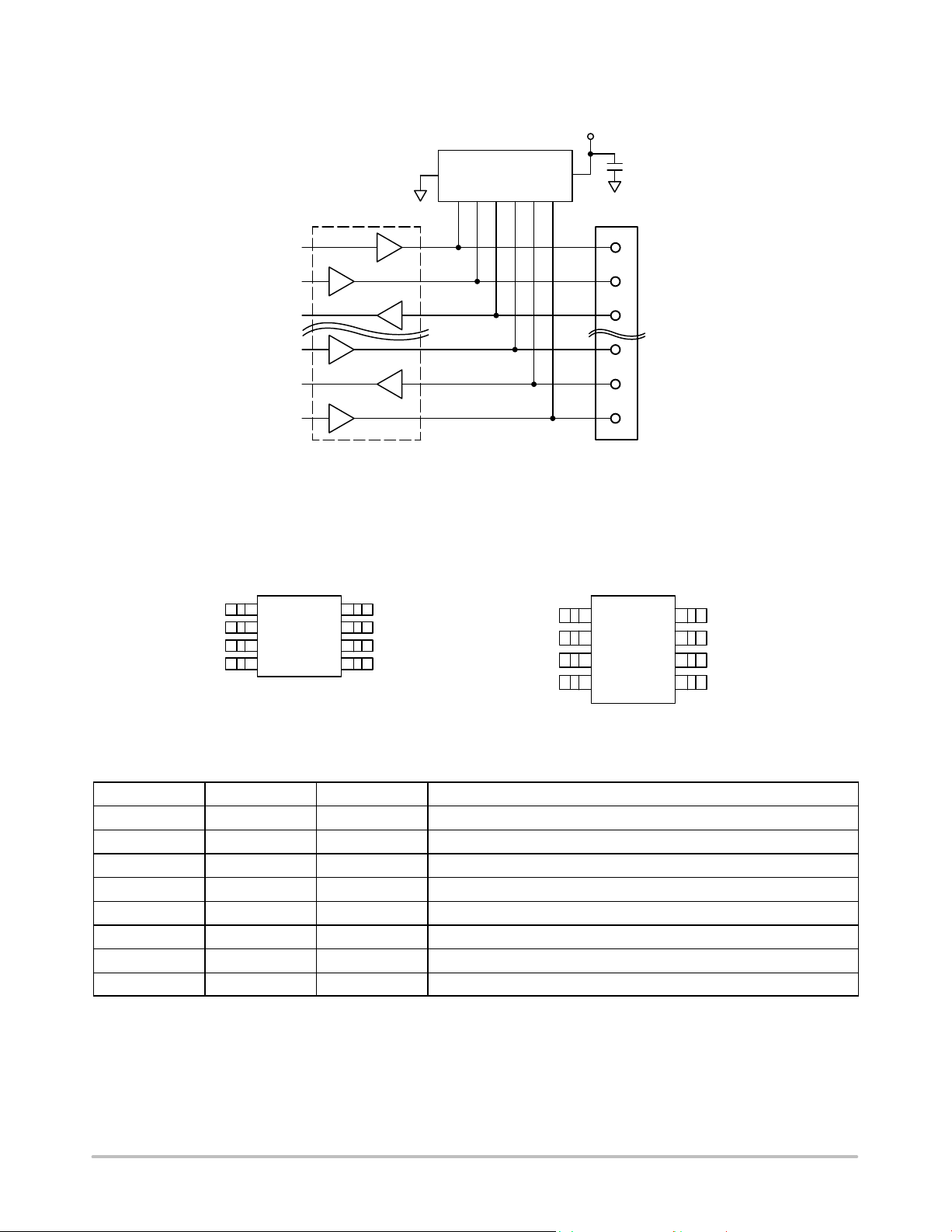
TYPICAL APPLICATION CIRCUIT
V
CC
CH1
CH2
V
CH3
N
I/O Port
Buffers
* Decoupling capacitor must be placed as close as possible to Pin7.
Top View
1
27
006R
8
36
4
5
8−Pin MSOP−8
37
PACDN006
2 4 5 6 81
Handheld/PDA ESD Protection
PACKAGE / PINOUT DIAGRAMS
CH6
V
P
CH5
CH4
CH1
CH2
V
CH3
N
0.22 mF*
Expansion
Connector
Top View
PACDN 006SM
1
8
27
36
4
5
CH6
V
P
CH5
CH4
8−Pin SOIC−8
Table 1. PIN DESCRIPTIONS
Pin Name Type Description
1 CH1 I/O ESD Channel
2 CH2 I/O ESD Channel
3 V
N
4 CH3 I/O ESD Channel
5 CH4 I/O ESD Channel
6 CH5 I/O ESD Channel
7 V
P
8 CH6 I/O ESD Channel
GND Negative Voltage Supply Rail or Ground Reference Rail
Supply Positive Voltage Supply Rail
http://onsemi.com
2

PACDN006
SPECIFICATIONS
Table 2. ABSOLUTE MAXIMUM RATINGS
Parameter Rating Units
Supply Voltage (VP − VN) 6.0 V
Diode Forward DC Current (Note 1) 20 mA
Operating Temperature Range −40 to +85 C
Storage Temperature Range −65 to +150 C
DC Voltage at any Channel Input (VN − 0.5) to (VP + 0.5) V
Package Power Rating 200 mW
Stresses exceeding Maximum Ratings may damage the device. Maximum Ratings are stress ratings only. Functional operation above the
Recommended Operating Conditions is not implied. Extended exposure to stresses above the Recommended Operating Conditions may affect
device reliability.
1. Only one diode conducting at a time.
Table 3. STANDARD OPERATING CONDITIONS
Parameter Rating Units
Operating Temperature Range −40 to +85 C
Operating Supply Voltage (VP − VN) 0 to 5.5 V
Table 4. ELECTRICAL OPERATING CHARACTERISTICS (Note 1)
Symbol
I
V
I
LEAK
C
V
ESD
P
Supply Current (VP − VN) = 5.5 V 10
Diode Forward Voltage I
F
Channel Leakage Current 0.1 1.0
Channel Input Capacitance @ 1 MHz, VP = 5 V,
IN
ESD Protection
Peak Discharge Voltage at any
Channel Input, in System
a) Human Body Model,
MIL−STD−883, Method 3015
b) Contact Discharge per
IEC 61000−4−2
c) Air Discharge per IEC 61000−4−2
V
CL
Channel Clamp Voltage
Positive Transients
Negative Transients
1. All parameters specified at TA = 25C unless otherwise noted. VP = 5 V, VN = 0 V unless noted.
2. From I/O pins to V
3. Human Body Model per MIL−STD−883, Method 3015, C
4. Standard IEC 61000−4−2 with C
Parameter Conditions Min Typ Max Units
= 20 mA 0.65 0.95 V
F
V
= 0 V, VIN = 2.5 V
N
(Note 2)
(Note 3)
(Note 4)
(Note 4)
15
8
15
@ 15 kV ESD HBM
or VN only. VP bypassed to VN with a 0.22 mF ceramic capacitor (see Application Information for more details).
P
= 150 pF, R
Discharge
Discharge
= 100 pF, R
Discharge
= 330 W, VP = 5.0 V, VN grounded.
Discharge
= 1.5 kWVP = 5.0 V, V
mA
mA
3 5 pF
kV
VP + 13.0
VN − 13.0
grounded.
N
V
http://onsemi.com
3
 Loading...