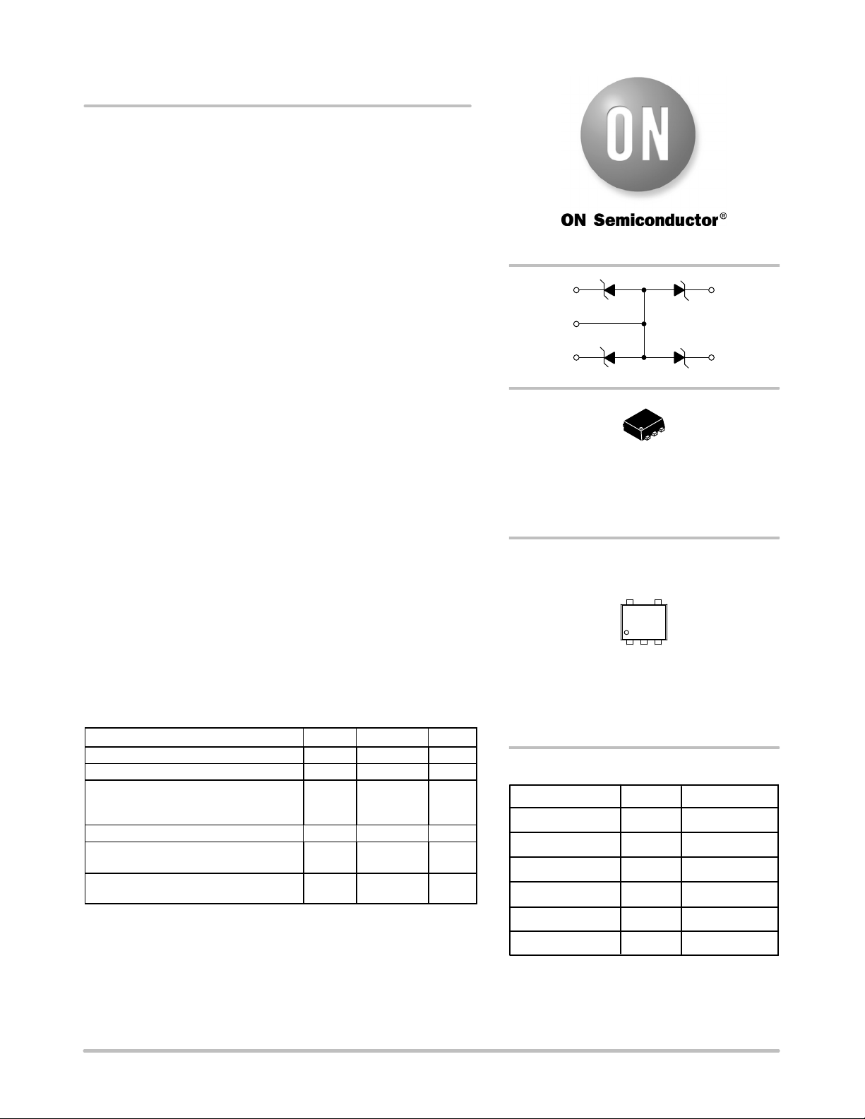
ON NZQA5V6AXV5, NZQA6V8AXV5 Schematic [ru]

NZQA5V6AXV5 Series
Transient Voltage Suppressors
ESD Protection Diode with Low Clamping
Voltage
This integrated transient voltage suppressor device (TVS) is
designed for applications requiring transient overvoltage protection. It
is intended for use in sensitive equipment such as computers, printers,
business machines, communication systems, medical equipment, and
other applications. Its integrated design provides very effective and
reliable protection for four separate lines using only one package.
These devices are ideal for situations where board space is at a premium.
Features
• Low Clamping Voltage
• Small SOT−553 SMT Package
• Stand Off Voltage: 3 V
• Low Leakage Current
• Four Separate Unidirectional Configurations for Protection
• ESD Protection: IEC61000−4−2: Level 4 ESD Protection
MILSTD 883C − Method 3015−6: Class 3
• Complies to USB 1.1 Low Speed & Full Speed Specifications
• These are Pb−Free Devices
Benefits
• Provides Protection for ESD Industry Standards: IEC 61000, HBM
• Protects Four Lines Against Transient Voltage Conditions
• Minimize Power Consumption of the System
• Minimize PCB Board Space
Typical Applications
• Instrumentation Equipment
• Serial and Parallel Ports
• Microprocessor Based Equipment
• Notebooks, Desktops, Servers
• Cellular and Portable Equipment
MAXIMUM RATINGS (T
Characteristic Symbol Value Unit
Peak Power Dissipation (Note 1) P
Steady State Power − 1 Diode (Note 2) P
Thermal Resistance,
Junction−to−Ambient
Above 25°C, Derate
Maximum Junction Temperature T
Operating Junction and Storage
Temperature Range
Lead Solder Temperature (10 seconds
duration)
Stresses exceeding Maximum Ratings may damage the device. Maximum
Ratings are stress ratings only. Functional operation above the Recommended
Operating Conditions is not implied. Extended exposure to stresses above the
Recommended Operating Conditions may affect device reliability.
1. Non−repetitive current per Figure 5.
2. Only 1 diode under power. For all 4 diodes under power, PD will be 25%.
Mounted on FR−4 board with min pad.
See Application Note AND8308/D for further description of
survivability specs.
= 25°C unless otherwise noted)
A
PK
D
R
q
JA
Jmax
TJ T
stg
T
L
20 W
380 mW
327
3.05
150 °C
−55 to
+150
260 °C
mW/°C
°C/W
°C
http://onsemi.com
1
2
3
SOT−553
CASE 463B
PLASTIC
5
4
MARKING DIAGRAM
xx M G
G
xx = Device Code
M = Date Code*
G = Pb−Free Package
(Note: Microdot may be in either location)
ORDERING INFORMATION
Device Package Shipping
NZQA5V6AXV5T1 SOT−553* 4000/Tape & Reel
NZQA5V6AXV5T1G SOT−553* 4000/Tape & Reel
NZQA6V8AXV5T1 SOT−553* 4000/Tape & Reel
NZQA6V8AXV5T1G SOT−553* 4000/Tape & Reel
NZQA6V8AXV5T3 16000/Tape & Reel
NZQA6V8AXV5T3G 16000/Tape & Reel
†For information on tape and reel specifications,
including part orientation and tape sizes, please
refer to our Tape and Reel Packaging Specification
Brochure, BRD8011/D.
*This package is inherently Pb−Free.
SOT−553*
SOT−553*
†
© Semiconductor Components Industries, LLC, 2009
September, 2009 − Rev. 7
1 Publication Order Number:
NZQA5V6AXV5/D

NZQA5V6AXV5 Series
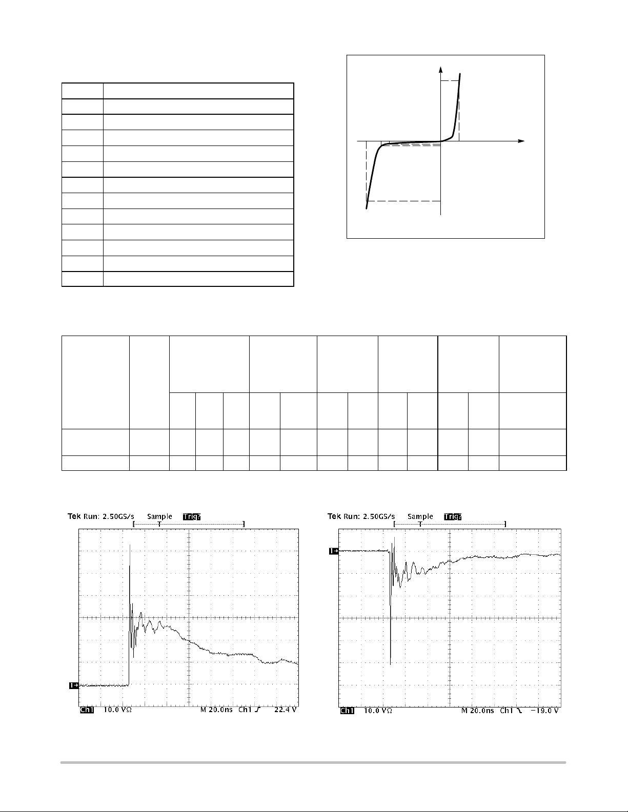
ELECTRICAL CHARACTERISTICS
(TA = 25°C unless otherwise noted)
Symbol Parameter
V
QV
I
PP
V
RWM
I
V
I
I
V
Z
I
ZK
Z
Maximum Reverse Peak Pulse Current
Clamping Voltage @ I
C
PP
Working Peak Reverse Voltage
Maximum Reverse Leakage Current @ V
R
Breakdown Voltage @ I
BR
Test Current
T
Maximum Temperature Coefficient of V
BR
Forward Current
F
Forward Voltage @ I
F
Maximum Zener Impedance @ I
ZT
F
Reverse Current
Maximum Zener Impedance @ I
ZK
T
ZT
ZK
BR
RWM
VCV
BR
V
RWM
I
I
F
I
V
R
F
I
T
I
PP
Uni−Directional
V
*See Application Note AND8308/D for detailed explanations of
datasheet parameters.
ELECTRICAL CHARACTERISTICS (T
Breakdown
Voltage
VBR @ 1 mA (V)
= 25°C)
A
Leakage
Current
IRM @ V
RM
VC Max @ I
(Note 4)
Capacitance
PP
Typ
@ 0 V Bias
(pF)
(Note 3)
Typ
Capacitance
@ 3 V Bias
(pF)
(Note 3)
V
C
Per
Device
Device
Marking
Min Nom Max V
RWM
I
RWM
(mA)
V
(V)
I
C
PP
(A)
Typ Max Typ Max
IEC61000−4−2
(Note 5)
NZQA5V6AXV5 5P 5.3 5.6 5.9 3.0 1.0 13 1.6 13 17 7.0 11.5 Figures 1 and 2
(See Below)
NZQA6V8AXV5 6H 6.47 6.8 7.14 4.3 1.0 13 1.6 12 15 6.7 9.5
3. Capacitance of one diode at f = 1 MHz, VR = 0 V, TA = 25°C
4. Surge current waveform per Figure 5.
5. For test procedure see Figures 3 and 4 and Application Note AND8307/D.
Figure 1. ESD Clamping Voltage Screenshot
Positive 8 kV Contact per IEC61000−4−2
http://onsemi.com
Figure 2. ESD Clamping Voltage Screenshot
Negative 8 kV Contact per IEC61000−4−2
2
 Loading...