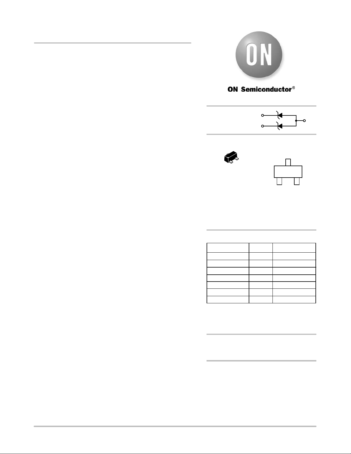
ON NZL5V6AXV3T1, NZL6V8AXV3T1, NZL7V5AXV3T1 Schematic [ru]

NZL5V6AXV3T1 Series
l
Preferred Devices
Dual Common Anode
ESD Protection Diodes
SC−89 Package
These dual monolithic silicon ESD protection diodes are intended for
use in voltage− and ESD−sensitive equipment such as computers,
printers, business machines, communication systems, medical
equipment and other applications. Their dual junction common anode
design protects two separate lines using only one package. These
devices are ideal for situations where board space is at a premium.
Specification Features:
• SC−89 Package Allows Either Two Separate Unidirectional
Configurations or a Single Bidirectional Configuration
• ESD Rating of Class N (exceeding 16 kV) per the
Human Body Model
• Meets IEC61000−4−2 Level 4
• Low Leakage < 5.0 mA
• These are Pb−Free Devices
Mechanical Characteristics:
Void-free, Transfer-molded, Thermosetting Plastic
CASE:
Epoxy Meets UL 94, V−0
LEAD FINISH: 100% Matte Sn (Tin)
MOUNTING POSITION: Any
QUALIFIED MAX REFLOW TEMPERATURE:
260°C Device Meets MSL 1 Requirements
http://onsemi.com
PIN 1. CATHODE
2. CATHODE
3. ANODE
1
3
2
MARKING
DIAGRAM
3
1
Lx G
G
2
M
SC−89
CASE 463C
STYLE 4
L = Device Code
x = Specific Device
M = Date Code
G = Pb−Free Package
(Note: Microdot may be in either location)
ORDERING INFORMATION
Device Package Shipping
NZL5V6AXV3T1 SC−89* 3000/Tape & Reel
NZL5V6AXV3T1G SC−89* 3000/Tape & Reel
NZL6V8AXV3T1 SC−89*
NZL6V8AXV3T3G SC−89*
NZL7V5AXV3T1
NZL7V5AXV3T1G SC−89*
†For information on tape and reel specifications,
including part orientation and tape sizes, please
refer to our Tape and Reel Packaging Specification
Brochure, BRD8011/D.
*This package is inherently Pb−Free.
SC−89*
3000/Tape & Reel
3000/Tape & ReelNZL6V8AXV3T1G SC−89*
10000/Tape & Ree
3000/Tape & Reel
3000/Tape & Reel
†
DEVICE MARKING INFORMATION
See specific marking information in the device marking
column of the table on page 2 of this data sheet.
© Semiconductor Components Industries, LLC, 2007
February, 2007 − Rev. 5
Preferred devices are recommended choices for future use
and best overall value.
1 Publication Order Number:
NZL5V6AXV3T1/D

NZL5V6AXV3T1 Series
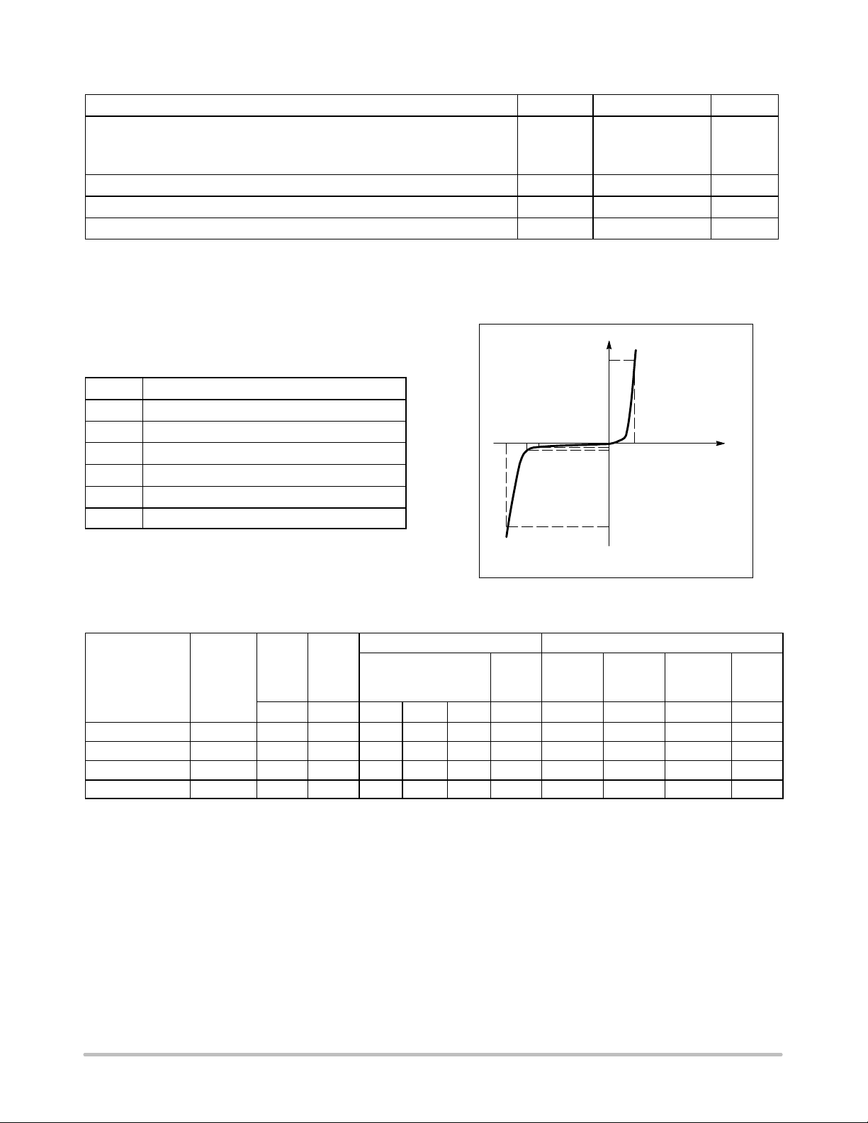
MAXIMUM RATINGS
Rating Symbol Value Unit
Total Power Dissipation on FR−5 Board (Note 1) @ TA = 25°C
Derate above 25°C
Thermal Resistance Junction to Ambient
Junction and Storage Temperature Range TJ, T
Lead Solder Temperature − Maximum (10 Second Duration) T
IEC61000−4−2 (Contact) 10 kV
Stresses exceeding Maximum Ratings may damage the device. Maximum Ratings are stress ratings only. Functional operation above the
Recommended Operating Conditions is not implied. Extended exposure to stresses above the Recommended Operating Conditions may affect
device reliability.
1. FR−5 board with minimum recommended mounting pad.
*Other voltages may be available upon request.
°PD° 240
1.9
R
q
JA
stg
L
525 °C/W
−55 to +150 °C
260 °C
°mW°
mW/°C
ELECTRICAL CHARACTERISTICS
(TA = 25°C unless otherwise noted)
UNIDIRECTIONAL (Circuit tied to Pins 1 and 3 or 2 and 3)
I
I
F
Symbol Parameter
V
RWM
I
V
I
I
V
Working Peak Reverse Voltage
Maximum Reverse Leakage Current @ V
R
Breakdown Voltage @ I
BR
Test Current
T
Forward Current
F
Forward Voltage @ I
F
F
RWM
T
VCV
BR
V
RWM
I
V
R
F
I
T
I
PP
V
Uni−Directional TVS
ELECTRICAL CHARACTERISTICS (T
= 25°C unless otherwise noted, VF = 0.9 V Max @ IF = 10 mA for all types)
A
UNIDIRECTIONAL (Circuit tied to Pins 1 and 3 or Pins 2 and 3)
Breakdown Voltage Surge
VC (V) @
T
IPP = 1.0
A
Device
Device
Marking
V
RWM
V
IR @
V
RWM
mA
V
(Note 2) (V) @ Iz
BR
Min Nom Max mA Typ Max Typ
NZL5V6AXV3T1 L0 3.0 5.0 5.32 5.6 5.88 5.0 7.0 10.1 4.8 50
NZL6V8AXV3T1 L2 4.5 1.0 6.46 6.8 7.14 5.0 7.9 11.9 6.7 73
NZL6V8AXV3T3 L2 4.5 1.0 6.46 6.8 7.14 5.0 7.9 11.9 6.7 73
NZL7V5AXV3T1 L3 5.0 1.0 7.12 7.5 7.88 5.0 8.8 13.5 5.7 75
2. VBR measured at pulse test current IT at an ambient temperature of 25°C.
† Surge current waveform per Figure 5.
VC (V) @
†
Max I
PP
Max I
PP
(A)
†
†
P
(W)
pk
†
http://onsemi.com
2

NZL5V6AXV3T1 Series
BREAKDOWN VOLTAGE (VOLTS) (V
@ I
)
5
CAPACITANCE (pF)
TYPICAL CHARACTERISTICS
T
9.0
250
BR
8.0
7.0
6.0
5.0
−55 +45
−5
TEMPERATURE (°C)
7V5
6V8
5V6
+95 +145
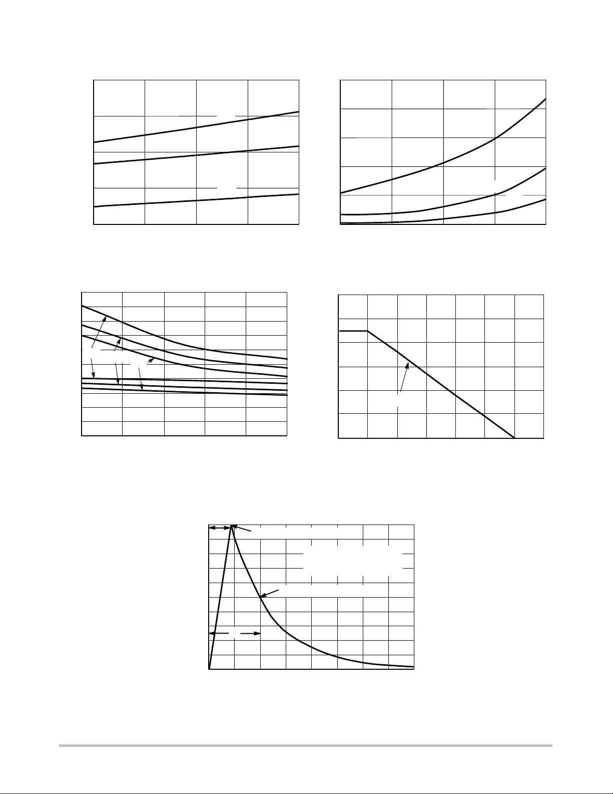
Figure 1. Typical Breakdown Voltage
versus Temperature
50
45
40
35
30
5V6
6V8
25
20
15
10
5
0
0 0.4 0.8 1.2 1.6 2.0
7V5
VOLTAGE (V)
Figure 3. Typical Capacitance versus Bias Voltage
(Upper curve for each part is unidirectional mode,
lower curve is bidirectional mode)
200
150
(nA)
R
I
100
50
0
−55 −5
TEMPERATURE (°C)
5V6
6V8
+45 +95
Figure 2. Typical Leakage Current
versus Temperature
300
250
200
150
100
, POWER DISSIPATION (mW)
50
D
P
0
0 25 50 75 100 125 150 175
FR−5 BOARD
TEMPERATURE (°C)
Figure 4. Steady State Power Derating Curve
7V5
+14
100
t
r
90
80
70
60
50
40
30
20
% OF PEAK PULSE CURRENT
10
0
020406080
t
P
PEAK VALUE I
HALF VALUE I
@ 8 ms
RSM
PULSE WIDTH (tP) IS DEFINED
AS THAT POINT WHERE THE
PEAK CURRENT DECAY = 8 ms
/2 @ 20 ms
RSM
t, TIME (ms)
Figure 5. 8 X 20 ms Pulse Waveform
http://onsemi.com
3
 Loading...