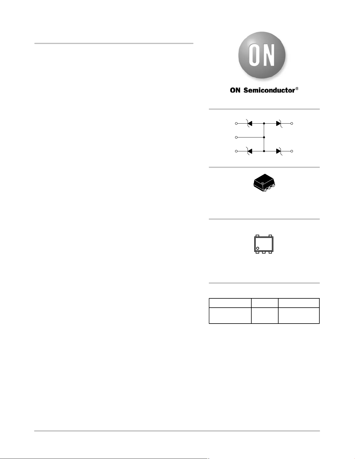
ON NUP46V8P5 Schematic [ru]

NUP46V8P5
Low Capacitance
Quad Array for
ESD Protection
This integrated transient voltage suppressor device (TVS) is
designed for applications requiring transient overvoltage protection. It
is intended to be used in sensitive equipment such as wireless headsets,
PDAs, digital cameras, computers, printers, communication systems,
and other applications. The integrated design provides very effective
and reliable protection for four separate lines using only one package.
This device is ideal for situations where board space is at a premium.
http://onsemi.com
1
2
5
Features
•ESD Protection: IEC61000-4-2: Level 4
•Four Separate Unidirectional Configurations for Protection
•Low Leakage Current < 1 mA @ 3 V
•Small SOT-953 SMT Package
•Low Capacitance
•This is a Pb-Free Device
Benefits
•Provides Protection for ESD Industry Standards: IEC 61000, HBM
•Protects Four Lines Against Transient Voltage Conditions
•Minimize Power Consumption of the System
•Minimize PCB Board Space
Typical Applications
•Cellular and Portable Electronics
•Serial and Parallel Ports
•Microprocessor Based Equipment
•Notebooks, Desktops, Servers
3
SOT-953
CASE 526AB
MARKING DIAGRAM
6 M
1
6 = Specific Device Code
M = Date Code
ORDERING INFORMATION
Device Package Shipping
NUP46V8P5T5G SOT-953
(Pb-Free)
4
†
8000 /
Tape & Reel
© Semiconductor Components Industries, LLC, 2008
January, 2008 - Rev. 0
†For information on tape and reel specifications,
including part orientation and tape sizes, please
refer to our Tape and Reel Packaging Specification
Brochure, BRD8011/D.
1 Publication Order Number:
NUP46V8P5/D

NUP46V8P5
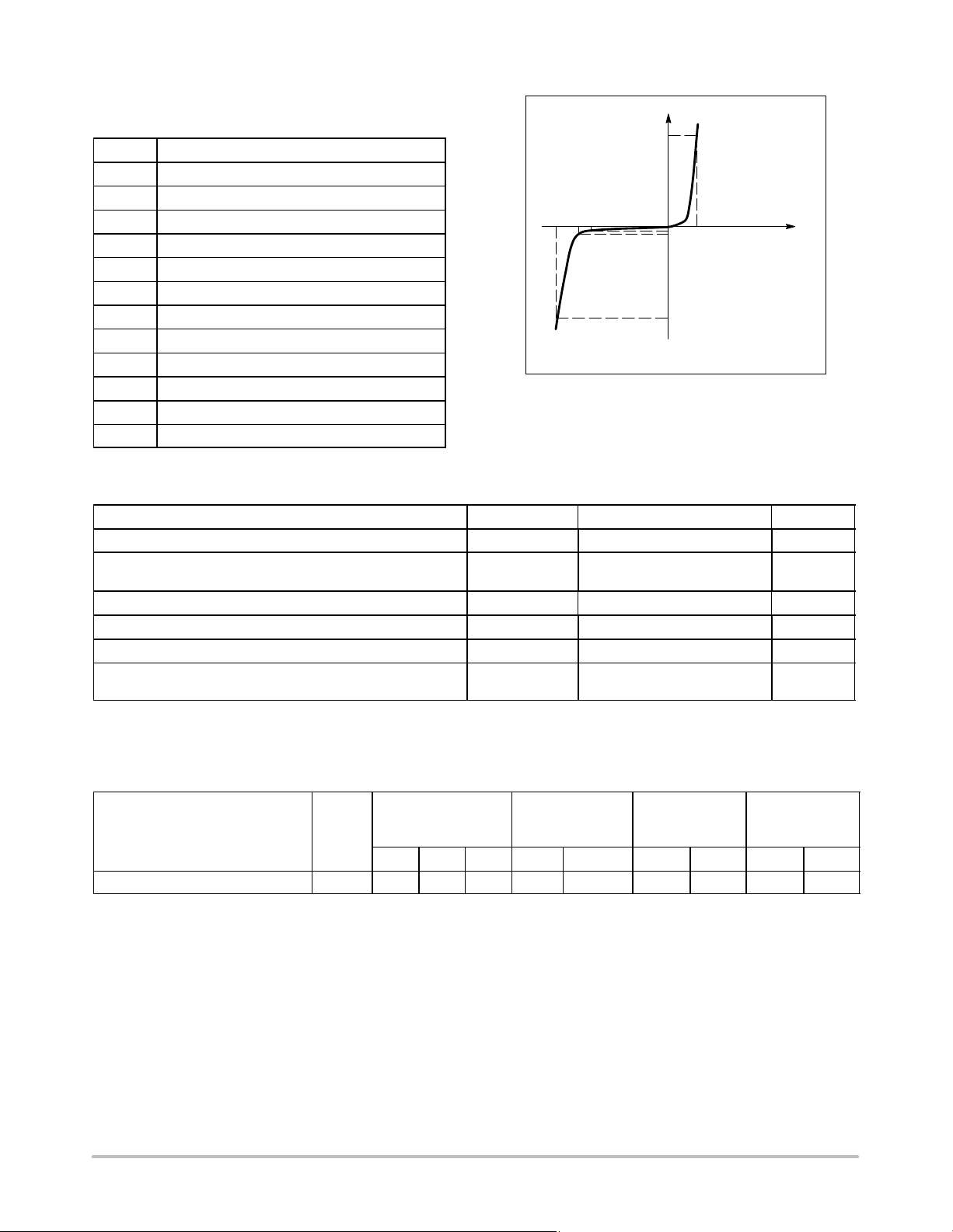
ELECTRICAL CHARACTERISTICS
(TA = 25°C unless otherwise noted)
Symbol
V
QV
I
V
RWM
V
V
Z
I
Z
Maximum Reverse Peak Pulse Current
PP
Clamping Voltage @ I
C
Working Peak Reverse Voltage
I
Maximum Reverse Leakage Current @ V
R
Breakdown Voltage @ I
BR
I
Test Current
T
Maximum Temperature Coefficient of V
BR
I
Forward Current
F
Forward Voltage @ I
F
Maximum Zener Impedance @ I
ZT
Reverse Current
ZK
Maximum Zener Impedance @ I
ZK
MAXIMUM RATINGS (T
Parameter
PP
T
F
= 25°C unless otherwise noted)
A
ZT
ZK
BR
RWM
VCV
BR
V
RWM
I
I
F
I
V
R
F
I
T
I
PP
Uni-Directional
V
Characteristic Symbol Value Unit
Peak Power Dissipation (8 X 20 ms @ TA = 25°C) (Note 1)
Thermal Resistance Junction-to-Ambient
P
R
Above 25°C, Derate
Maximum Junction Temperature T
Jmax
Operating Junction and Storage Temperature Range TJ T
Lead Solder Temperature (10 seconds duration) T
Human Body Model (HBM)
ESD 8000
Machine Model (MM)
PK
q
JA
stg
L
10 W
560
4.5
°C/W
mW/°C
150 °C
-55 to +150 °C
260 °C
400
V
Stresses exceeding Maximum Ratings may damage the device. Maximum Ratings are stress ratings only. Functional operation above the
Recommended Operating Conditions is not implied. Extended exposure to stresses above the Recommended Operating Conditions may affect
device reliability.
ELECTRICAL CHARACTERISTICS (T
Device
= 25°C)
A
Device
Marking
Breakdown Voltage
@ 1 mA (Volts)
V
BR
Min Nom Max V
Leakage Current
@ V
I
RM
RM
I
RWM
(mA)
RWM
Typ Capacitance
@ 0 V Bias (pF)
(Note 2)
Typ Capacitance
@ 3 V Bias (pF)
(Note 2)
Typ Max Typ Max
NUP46V8P5 6 6.47 6.8 7.14 4.3 1.0 12 15 6.7 9.5
1. Non-repetitive current per Figure 1.
2. Capacitance of one diode at f = 1 MHz, V
= 0 V, TA = 25°C.
R
http://onsemi.com
2
 Loading...