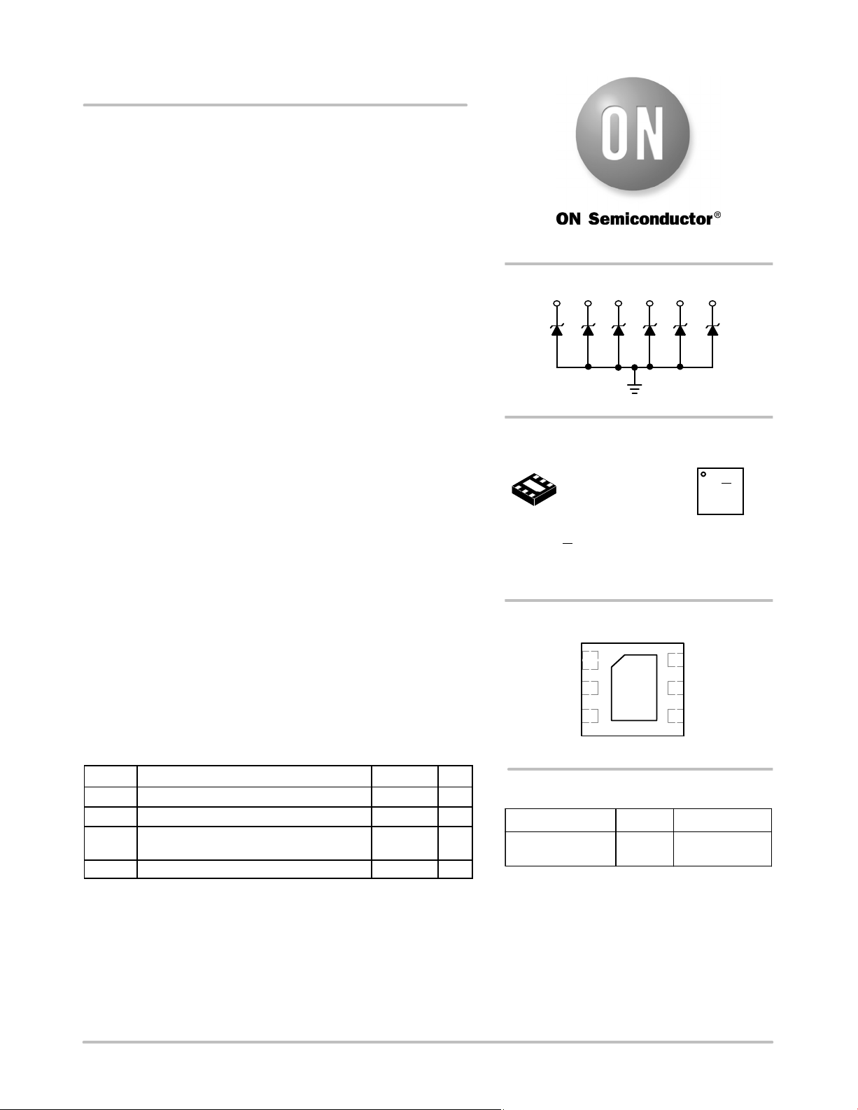
ON NUP4212UPMU Schematic [ru]

NUP4212UPMU
Quad Transient Voltage
Suppressor Array
ESD Protection Diodes with Ultra−Low
(0.7 pF) Capacitance
The four−line voltage transient suppressor array is designed to protect
voltage−sensitive components that require ultra−low capacitance from
ESD and transient voltage events. This device features a common anode
design which can protect up to four independent high speed data lines
and 1 or 2 separate 15 V TVS lines in a single six−lead UDFN low
profile package.
Excellent clamping capability, low capacitance, low leakage, and fast
response time make these parts ideal for ESD protection on designs
where board space is at a premium. Because of its low capacitance, it is
suited for use in high frequency designs such as a USB 2.0 high speed.
This device can be configured as a dual port USB device.
Features
• Low Capacitance Data Lines (0.7 pF Typical)
• Protects up to Four Data Lines Plus a V
CC
Pin
• UDFN Package, 1.6 x 1.6 mm
• Low Profile of 0.50 mm for Ultra Slim Design
• V
, V2 Pin = 15 V Protection
1
• D
, D2, D3, and D4 Pins = 5.2 V Minimum Protection
1
• ESD Rating: IEC61000−4−2: Level 4
− Contact (14 kV)
• This is a Pb−Free Device
Typical Applications
• USB 2.0 High−Speed Interface
• Cell Phones
• MP3 Players
• SIM Card Protection
http://onsemi.com
D1D2D3D4V
1
MARKING
DIAGRAM
UDFN6 1.6 X 1.6
6
MU SUFFIX
1
(Note: Microdot may be in either location)
CASE 517AP
P2 = Specific Device Code
M
= Date Code
G = Pb−Free Package
1
PIN CONNECTIONS
6
D
1
1
D
2
D
3
GND
2
3
V
2
V
5
1
D
4
4
V
2
P2 MG
G
MAXIMUM RATINGS (T
Symbol Rating Value Unit
T
J
T
STG
T
L
ESD IEC 61000−4−2 Contact 14000 V
Stresses exceeding Maximum Ratings may damage the device. Maximum
Ratings are stress ratings only. Functional operation above the Recommended
Operating Conditions is not implied. Extended exposure to stresses above the
Recommended Operating Conditions may affect device reliability.
Operating Junction Temperature Range −40 to 125 °C
Storage Temperature Range −55 to 150 °C
Lead Solder Temperature – Maximum
(10 seconds)
= 25°C, unless otherwise specified)
J
260 °C
NUP4212UPMUTAG UDFN6
†For information on tape and reel specifications,
including part orientation and tape sizes, please
refer to our Tape and Reel Packaging Specification
Brochure, BRD8011/D.
See Application Note AND8308/D for further description of survivability specs.
© Semiconductor Components Industries, LLC, 2009
August, 2009− Rev. 1
1 Publication Order Number:
ORDERING INFORMATION
Device Package Shipping
3000/Tape & Reel
(Pb−Free)
NUP4212UPMU/D
†

NUP4212UPMU
ELECTRICAL CHARACTERISTICS
(TA = 25°C unless otherwise noted)
Symbol
V
I
V
RWM
V
V
P
Maximum Reverse Peak Pulse Current
PP
Clamping Voltage @ I
C
Working Peak Reverse Voltage
I
Maximum Reverse Leakage Current @ V
R
Breakdown Voltage @ I
BR
I
Test Current
T
I
Forward Current
F
Forward Voltage @ I
F
Peak Power Dissipation
pk
C Max. Capacitance @ VR = 0 and f = 1.0 MHz
*See Application Note AND8308/D for detailed explanations of
datasheet parameters.
ELECTRICAL CHARACTERISTICS (T
Parameter Conditions Symbol Min Typ Max Unit
Reverse Working Voltage (D1, D2, D
Reverse Working Voltage (V1 and V2) (Note 1) V
Breakdown Voltage (D1, D2, D
Breakdown Voltage (V1, V2) IT = 5 mA, (Note 2) V
Reverse Leakage Current (D1, D2, D
Reverse Leakage Current (V1, V2) @ V
Capacitance (D1, D2, D
Clamping Voltage @ IPP = 1 A (Note 3) V
Clamping Voltage Per IEC61000−4−2 (Note 4) V
1. TVS devices are normally selected according to the working peak reverse voltage (V
or continuous peak operating voltage level.
is measured at pulse test current IT.
2. V
BR
3. Surge current waveform per Figure 5.
4. Typical waveform. For test procedure see Figures 3 and 4 and Application Note AND8307/D.
Parameter
PP
V
VCV
RWM
T
F
BR
RWM
Uni−Directional TVS
= 25°C, unless otherwise specified)
J
and D4) (Note 1) V
3,
and D4) IT = 1 mA, (Note 2) V
3,
and D4) @ V
3,
and D4) VR = 0 V, f = 1 MHz (Line to GND) C
3,
RWM1
RWM2
), which should be equal or greater than the DC
RWM
I
RWM1
RWM2
BR
BR2
I
R
I
R
J
C
C
I
F
I
V
R
F
I
T
I
PP
− − 4.0 V
− − 12 V
5.2 5.5 − V
13.5 15 15.8 V
− − 1.0
− − 1.0
− 0.7 0.9 pF
− − 14.3 V
Figures 1 and 2 V
V
mA
mA
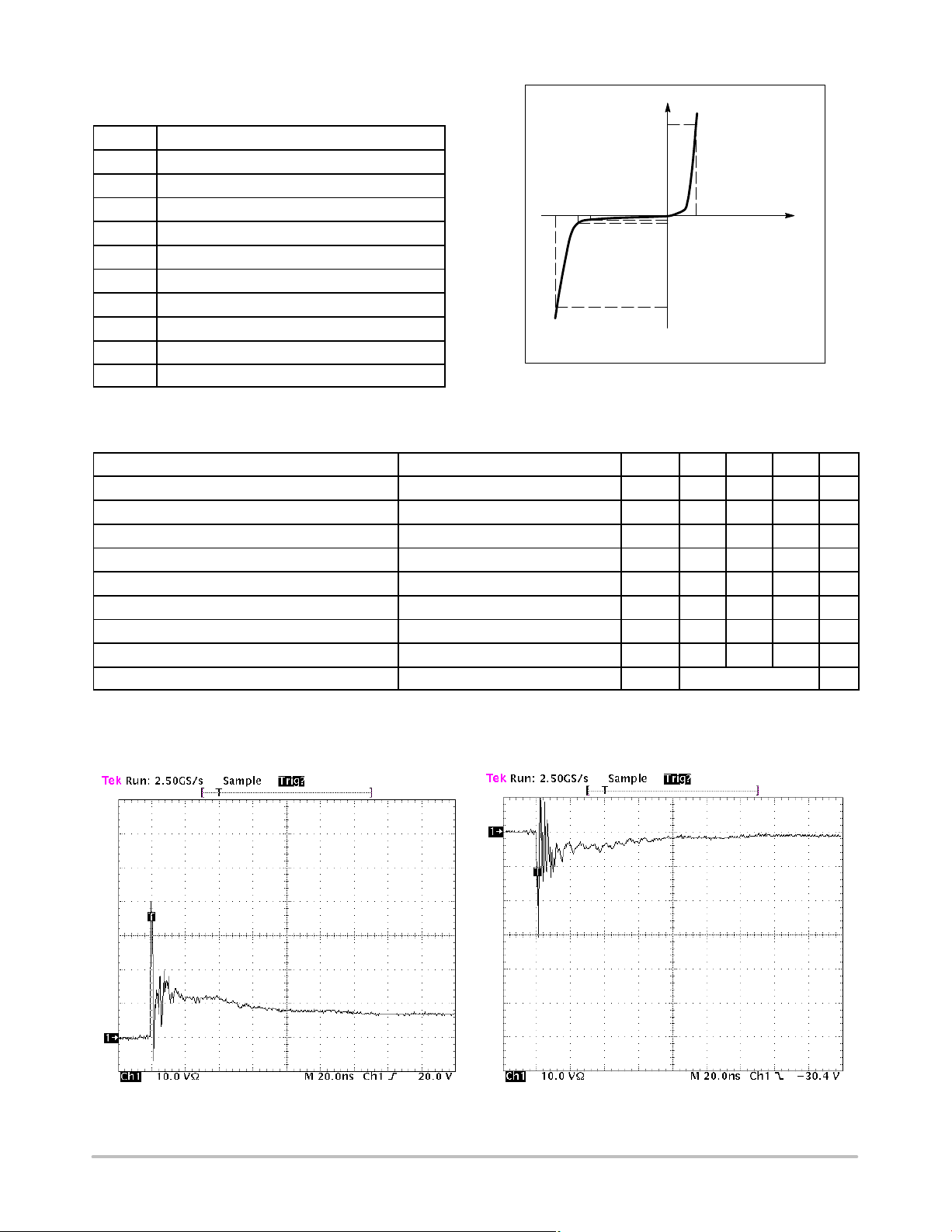
Figure 1. ESD Clamping Voltage Screenshot
Positive 8 kV Contact per IEC61000−4−2
http://onsemi.com
Figure 2. ESD Clamping Voltage Screenshot
Negative 8 kV Contact per IEC61000−4−2
2
 Loading...