ON NUP4106 Schematic [ru]

NUP4106
Low Capacitance Surface
Mount TVS for High-Speed
Data Interfaces
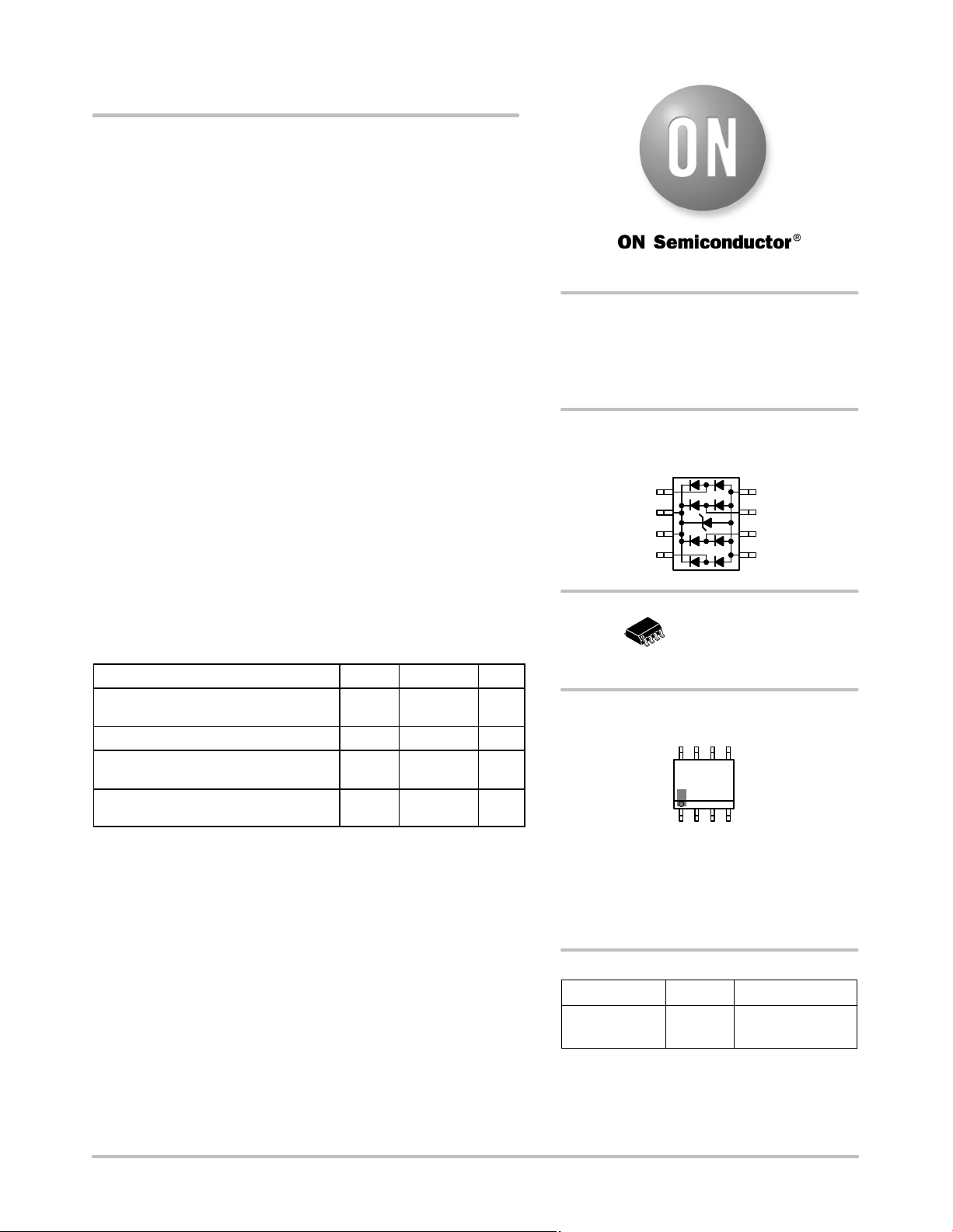
The NUP4106 transient voltage suppressor is designed to protect
equipment attached to high speed communication lines from ESD and
lightning.
http://onsemi.com
Features
• SO−8 Package
• Peak Power − 500 W 8 x 20 mS
• ESD Rating:
IEC 61000−4−2 (ESD) 15 kV (air) 8 kV (contact)
• UL Flammability Rating of 94 V−0
• This is a Pb−Free Device
Typical Applications
• High Speed Communication Line Protection
• T1/E1 Secondary Protection
• T3/E3 Secondary Protection
• Analog Video Protection
• Base Stations
2
• I
C Bus Protection
MAXIMUM RATINGS
Rating Symbol Value Unit
Peak Power Dissipation
8 x 20 mS @ T
Junction and Storage Temperature Range TJ, T
Lead Solder Temperature −
Maximum 10 Seconds Duration
IEC 61000−4−2 Contact
Stresses exceeding Maximum Ratings may damage the device. Maximum
Ratings are stress ratings only. Functional operation above the Recommended
Operating Conditions is not implied. Extended exposure to stresses above the
Recommended Operating Conditions may affect device reliability.
1. Non−repetitive current pulse 8 x 20 mS exponential decay waveform
Pin 2/3 to Pin 5/8
= 25°C (Note 1)
A
Air
P
pk
stg
T
L
ESD ±8
500 W
−55 to +150 °C
260 °C
±15
kV
SO−8 LOW CAPACITANCE
VOLTAGE SUPPRESSOR
500 WATTS PEAK POWER
3.3 VOLTS
PIN CONFIGURATION
AND SCHEMATIC
I/O 1 1
REF 1 2
REF 1 3
I/O 2 4
8
1
MARKING DIAGRAM
8
P4106
AYWWG
G
1
A = Assembly Location
Y = Year
WW = Work Week
G = Pb−Free Package
(Note: Microdot may be in either location)
8 GND
7 I/O 4
6 I/O 3
5 GND
SOIC−8
CASE 751
PLASTIC
© Semiconductor Components Industries, LLC, 2009
February, 2009 − Rev. 0
ORDERING INFORMATION
Device Package
NUP4106DR2G SO−8
(Pb−Free)
†For information on tape and reel specifications,
including part orientation and tape sizes, please
refer to our Tape and Reel Packaging Specification
Brochure, BRD8011/D.
1 Publication Order Number:
Shipping
2500/Tape & Reel
†
NUP4106/D

NUP4106
ELECTRICAL CHARACTERISTICS
Characteristic Symbol Min Typ Max Unit
Reverse Breakdown Voltage @ It = 1.0 mA V
Reverse Leakage Current @ V
= 3.3 V I
RWN
Maximum Clamping Voltage @ IPP = 1.0 A, 8 x 20 mS
Maximum Clamping Voltage @ IPP = 10 A, 8 x 20 mS
Maximum Clamping Voltage @ IPP = 25 A, 8 x 20 mS
BR
R
V
C
V
C
V
C
Between I/O Pins and Ground @ VR = 0 V, 1.0 MHz Capacitance − 8.0 15 pF
Between I/O Pins @ VR = 0 Volts, 1.0 MHz Capacitance − 4.0 − pF
5.0 − − V
N/A − 5.0
N/A − 7.0 V
N/A − 10 V
N/A − 15 V
mA
ELECTRICAL CHARACTERISTICS
(TA = 25°C unless otherwise noted)
Symbol
I
PP
V
C
V
RWM
I
R
V
BR
I
T
I
F
V
F
P
pk
Maximum Reverse Peak Pulse Current
Clamping Voltage @ I
Working Peak Reverse Voltage
Maximum Reverse Leakage Current @ V
Breakdown Voltage @ I
Test Current
Forward Current
Forward Voltage @ I
Peak Power Dissipation
Parameter
PP
RWM
T
F
C Capacitance @ VR = 0 and f = 1.0 MHz
*See Application Note AND8308/D for detailed explanations of
datasheet parameters.
TYPICAL CHARACTERISTICS
100
t
r
90
80
70
60
50
40
30
20
% OF PEAK PULSE CURRENT
10
0
0204060
PEAK VALUE I
RSM
@ 8 ms
PULSE WIDTH (tP) IS DEFINED
AS THAT POINT WHERE THE
PEAK CURRENT DECAY = 8 ms
HALF VALUE I
t
P
/2 @ 20 ms
RSM
t, TIME (ms)
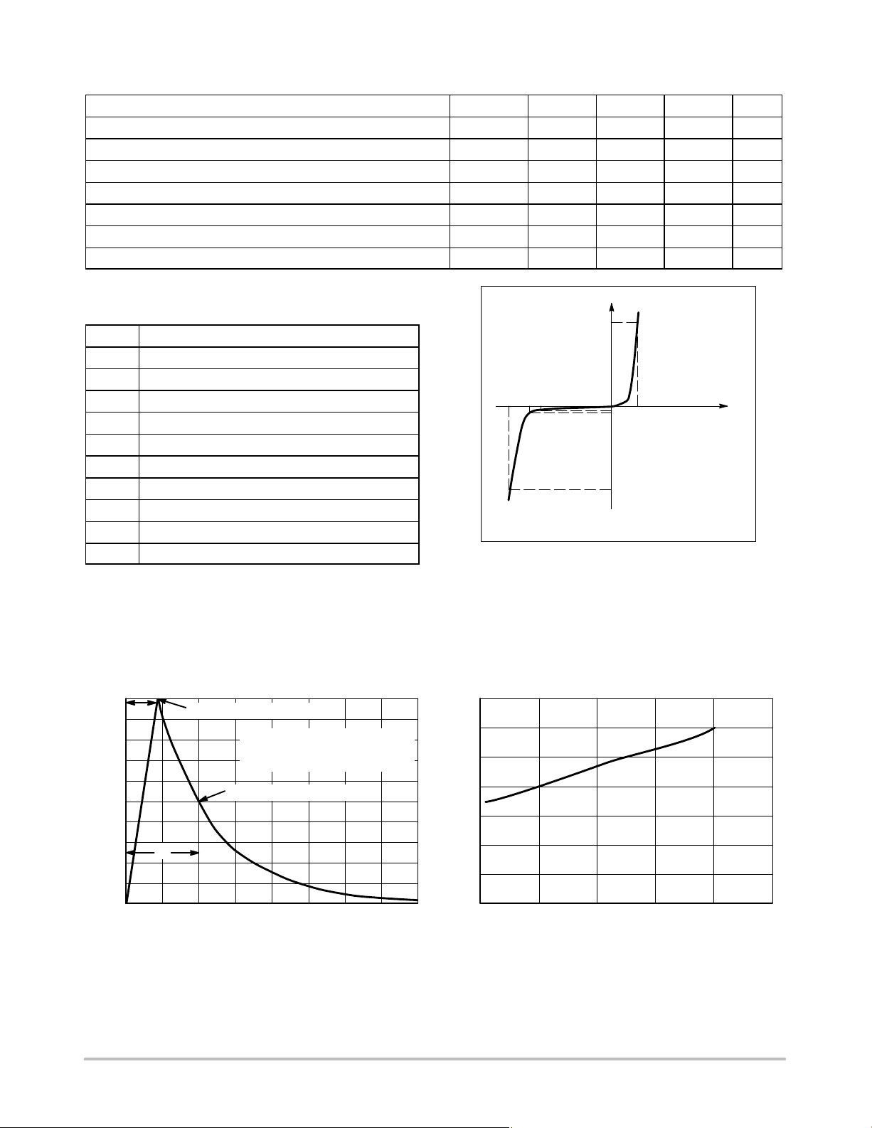
Figure 1. 8 x 20 ms Pulse Waveform
80
I
I
F
V
VCV
BR
RWM
I
V
R
F
I
T
I
PP
V
Uni−Directional TVS
14
12
10
8
6
4
CLAMPING VOLTAGE (V)
2
0
010
20 30 40 50
PEAK PULSE CURRENT (A)
Figure 2. Clamping Voltage vs. Peak Pulse Current
(8 x 20 ms Waveform)
http://onsemi.com
2

NUP4106
APPLICATIONS INFORMATION
The NUP4106 is a low capacitance TVS diode array
designed to protect sensitive electronics such as
communications systems, computers, and computer
peripherals against damage due to ESD events or transient
overvoltage conditions. Because of its low capacitance, it
can be used in high speed I/O data lines. The integrated
design of the NUP4106 offers surge rated, low capacitance
steering diodes and a TVS diode integrated in a single
package (SO−8). If a transient condition occurs, the steering
diodes will drive the transient to the positive rail of the
power supply or to ground. The TVS device protects the
power line against overvoltage conditions avoiding damage
to the power supply and other downstream components.
NUP4106 Configuration Options
The NUP4106 is able to protect up to four data lines
against transient overvoltage conditions by driving them to
a fixed reference point for clamping purposes. The steering
diodes will be forward biased whenever the voltage on the
protected line exceeds the reference voltage (Vf or
V
+ Vf). The diodes will force the transient current to
CC
bypass the sensitive circuit.
Data lines are connected at pins 1, 4, 6 and 7. The negative
reference is connected at pins 5 and 8. These pins must be
connected directly to ground using a ground plane to
minimize the PCB’s ground inductance. It is very important
to reduce the PCB trace lengths as much as possible to
minimize parasitic inductances.
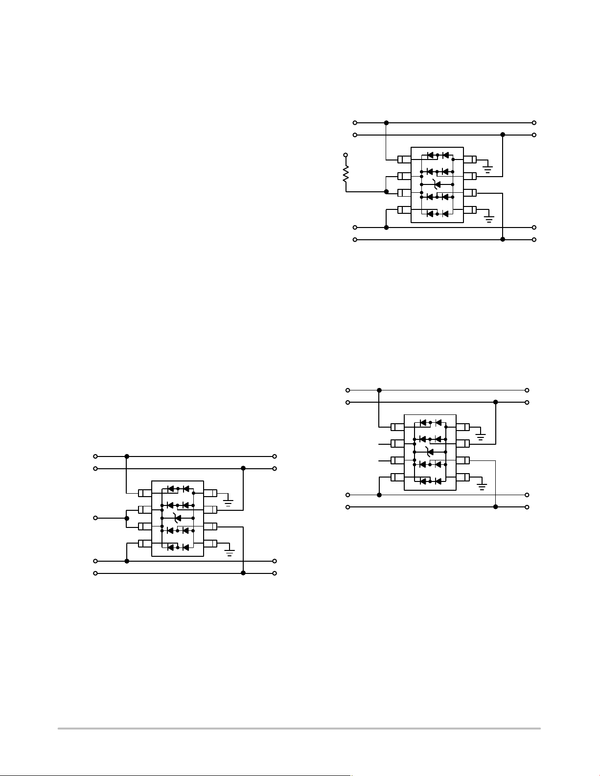
Option 1
Protection of four data lines and the power supply using
V
as reference.
CC
I/O 1
I/O 2
V
CC
I/O 3
I/O 4
1
2
3
4
Figure 3.
8
7
6
5
For this configuration, connect pins 2 and 3 directly to the
positive supply rail (V
). The data lines are referenced to
CC
the supply voltage. The internal TVS diode prevents
overvoltage on the supply rail. Biasing of the steering diodes
reduces their capacitance.
Option 2
Protection of four data lines with bias and power supply
isolation resistor.
I/O 1
I/O 2
V
CC
10 K
1
2
3
4
I/O 3
I/O 4
Figure 4.
8
7
6
5
The NUP4106 can be isolated from the power supply by
connecting a series resistor between pins 2 and 3 and V
CC
A 10 kW resistor is recommended for this application. This
will maintain a bias on the internal TVS and steering diodes,
reducing their capacitance.
Option 3
Protection of four data lines using the internal TVS diode
as reference.
I/O 1
I/O 2
I/O 3
I/O 4
NC
NC
1
2
3
4
Figure 5.
8
7
6
5
In applications lacking a positive supply reference or
those cases in which a fully isolated power supply is
required, the internal TVS can be used as the reference. For
these applications, pins 2 and 3 are not connected. In this
configuration, the steering diodes will conduct whenever the
voltage on the protected line exceeds the working voltage of
the TVS plus one diode drop (Vc=Vf + V
TVS).
.
http://onsemi.com
3
 Loading...