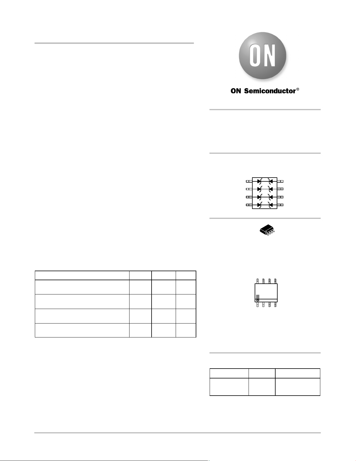
ON NUP4000 Schematic [ru]

NUP4000
Bi-directional TVS Array for
High-Speed Data Line
Protection
The NUP4000 transient voltage suppressor is designed to protect
equipment attached to up to four high speed communication lines from
ESD, EFT, and lightning.
Features:
• SO−8 Package
• Peak Power − 400 W 8 x 20 mS
• ESD Rating:
IEC 61000−4−2 (ESD) ±15 kV (air) ±8 kV (contact)
IEC 61000−4−4 (EFT) 40 A (5/50 ns)
IEC 61000−4−5 (lightning) 12 A (8/20 ms)
• UL Flammability Rating of 94 V−0
• These Devices are Pb−Free, Halogen Free/BFR Free and are RoHS
Compliant
Typical Applications:
• High Speed Communication Line Protection
• 15 V Data and I/O Lines
• Microprocessor Based Equipment
• LAN/WAN Equipment
• Servers
• Notebook and Desktop PC
• Serial and Parallel Ports
• Peripherals
http://onsemi.com
SO−8
VOLTAGE SUPPRESSOR
400 WATTS PEAK POWER
15 VOLTS
PIN CONFIGURATION
AND SCHEMATIC
1
2
3
4
8
SO−8
CASE 751
8
7
6
5
1
MAXIMUM RATINGS
Rating Symbol Value Unit
Peak Power Dissipation
8 x 20 ms @ T
Peak Pulse Current
8 x 20 ms @ T
Junction and Storage
Temperature Range
Lead Solder Temperature −
Maximum 10 Seconds Duration
1. Non−repetitive current pulse 8 x 20 mS exponential decay waveform
= 25°C (Note 1)
A
= 25°C (Note 1)
A
P
I
TJ, T
T
PP
stg
400 W
10 A
−55 to
+150
260 °C
pk
L
°C
MARKING DIAGRAM
8
NUP40
AYWWG
G
1
A = Assembly Location
Y = Year
WW = Work Week
G = Pb−Free Package
(Note: Microdot may be in either location)
ORDERING INFORMATION
Device Package Shipping
NUP4000DR2G SO−8
(Pb−Free)
†For information on tape and reel specifications,
including part orientation and tape sizes, please
refer to our Tape and Reel Packaging Specification
Brochure, BRD8011/D.
2500 / Tape & Reel
†
© Semiconductor Components Industries, LLC, 2009
August, 2009 − Rev. 0
1 Publication Order Number:
NUP4000/D

NUP4000
ELECTRICAL CHARACTERISTICS
Characteristic Symbol Min Typ Max Unit
Reverse Working Voltage V
Reverse Breakdown Voltage @ It = 1.0 mA V
Reverse Leakage Current @ V
Maximum Clamping Voltage @ IPP = 1.0 A, 8 x 20 mS
Maximum Clamping Voltage @ IPP = 5.0 A, 8 x 20 mS
Maximum Peak Pulse Current I
Junction Capacitance @ VR = 0 V, f = 1 MHz C
= 15 Volts I
RWM
RWM
BR
R
V
C
V
C
PP
J
− − 15 V
16.7 − − V
N/A − 1.0
N/A − 24 V
N/A − 30 V
− − 10 A
− − 75 pF
mA
1000
100
10
NOTE: Non−Repetitive Surge.
, PEAK SURGE POWER (WATTS)
pk
P
1
1 10 100 1000
t, TIME (ms)
Figure 1. Pulse Width
100
90
80
70
60
50
t
r
PEAK VALUE I
PULSE WIDTH (tP) IS DEFINED
AS THAT POINT WHERE THE
PEAK CURRENT DECAY = 8 ms
HALF VALUE I
RSM
@ 8 ms
RSM
/2 @ 20 ms
40
30
20
10
% OF PEAK PULSE CURRENT
0
t
P
020406080
t, TIME (ms)
Figure 2. 8 × 20 ms Pulse Waveform
http://onsemi.com
2
 Loading...