

NUP3112UPMU
Quad Transient Voltage
Suppressor Array
ESD Protection Diodes with Ultra−Low
(0.7 pF) Capacitance
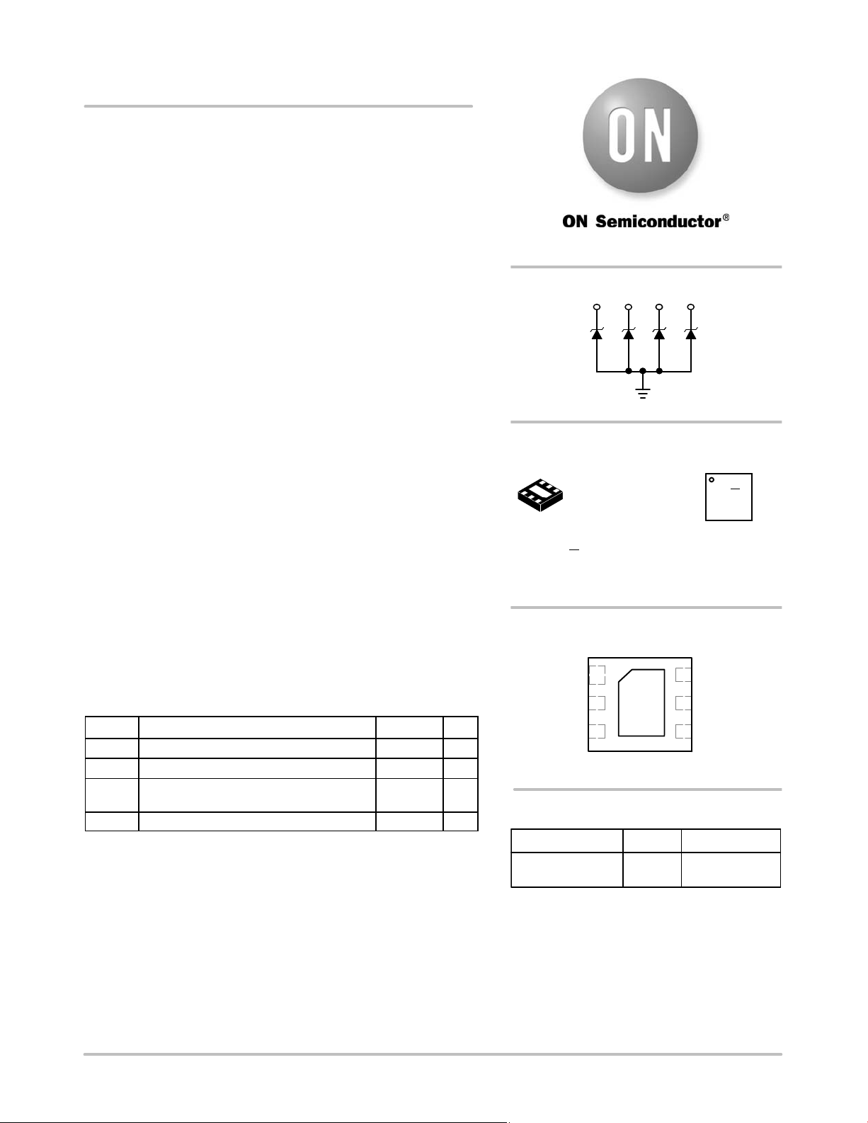
The three−line voltage transient suppressor array is designed to protect
voltage−sensitive components that require ultra−low capacitance from
ESD and transient voltage events. This device features a common anode
design which protects three independent high speed data lines and a V
CC
power line in a single six−lead UDFN low profile package.
Excellent clamping capability, low capacitance, low leakage, and fast
response time make these parts ideal for ESD protection on designs
where board space is at a premium. Because of its low capacitance, it is
suited for use in high frequency designs such as a USB 2.0 high speed.
Features
• Low Capacitance Data Lines (0.7 pF Typical)
• Protects up to Three Data Lines Plus a V
CC
Pin
• UDFN Package, 1.6 x 1.6 mm
• Low Profile of 0.50 mm for Ultra Slim Design
• ESD Rating: IEC61000−4−2: Level 4
− Contact (14 kV)
• V
Pin = 15 V Protection
CC
• D
, D2, and D3 Pins = 5.2 V Minimum Protection
1
• This is a Pb−Free Device
Typical Applications
• USB 2.0 High−Speed Interface
• Cell Phones
• MP3 Players
• SIM Card Protection
MAXIMUM RATINGS (T
Symbol
T
J
T
STG
T
L
ESD IEC 61000−4−2 Contact 14000 V
Stresses exceeding Maximum Ratings may damage the device. Maximum
Ratings are stress ratings only. Functional operation above the Recommended
Operating Conditions is not implied. Extended exposure to stresses above the
Recommended Operating Conditions may affect device reliability.
Operating Junction Temperature Range −40 to 125 °C
Storage Temperature Range −55 to 150 °C
Lead Solder Temperature – Maximum
(10 seconds)
= 25°C, unless otherwise specified)
J
Rating Value Unit
260 °C
http://onsemi.com
D1D2D3V
UDFN6 1.6x1.6
6
MU SUFFIX
1
(Note: Microdot may be in either location)
Device Package Shipping
NUP3112UPMUTAG UDFN6
†For information on tape and reel specifications,
including part orientation and tape sizes, please
refer to our Tape and Reel Packaging Specification
Brochure, BRD8011/D.
CASE 517AP
XX = Specific Device Code
M
= Date Code
G = Pb−Free Package
PIN CONNECTIONS
D
1
1
GND
2
D
2
3
D
3
ORDERING INFORMATION
(Pb−Free)
CC
MARKING
DIAGRAM
1
XX MG
G
6
V
CC
NC
5
NC
4
†
3000/Tape & Reel
© Semiconductor Components Industries, LLC, 2008
June, 2008− Rev. 0
1 Publication Order Number:
NUP3112UPMU/D
ELECTRICAL CHARACTERISTICS
(TA = 25°C unless otherwise noted)
Symbol
V
I
V
RWM
V
V
P
Maximum Reverse Peak Pulse Current
PP
Clamping Voltage @ I
C
Working Peak Reverse Voltage
I
Maximum Reverse Leakage Current @ V
R
Breakdown Voltage @ I
BR
I
Test Current
T
I
Forward Current
F
Forward Voltage @ I
F
Peak Power Dissipation
pk
C Max. Capacitance @ VR = 0 and f = 1.0 MHz
Parameter
PP
T
F
NUP3112UPMU
RWM
VCV
V
RWM
BR
Uni−Directional TVS
I
I
F
I
V
R
F
I
T
I
PP
V
ELECTRICAL CHARACTERISTICS (T
= 25°C, unless otherwise specified)
J
Parameter Conditions Symbol Min Typ Max Unit
Reverse Working Voltage (D1, D2, and D3) (Note 1) V
Reverse Working Voltage (V1) (Note 1) V
Breakdown Voltage (D1, D2, and D3) IT = 1 mA, (Note 2) V
Breakdown Voltage (VCC) IT = 5 mA, (Note 2) V
Reverse Leakage Current (D1, D2, and D3) @ V
Reverse Leakage Current (VCC) @ V
RWM
RWM2
Capacitance (D1, D2, and D3) VR = 0 V, f = 1 MHz (Line to GND) C
1. TVS devices are normally selected according to the working peak reverse voltage (V
or continuous peak operating voltage level.
is measured at pulse test current IT.
2. V
BR
), which should be equal or greater than the DC
RWM
RWM1
RWM2
BR
BR2
I
R
I
R
J
− − 4.0 V
− − 12 V
5.2 5.5 − V
13.5 15 15.8 V
− − 1.0
− − 1.0
− 0.7 0.9 pF
mA
mA
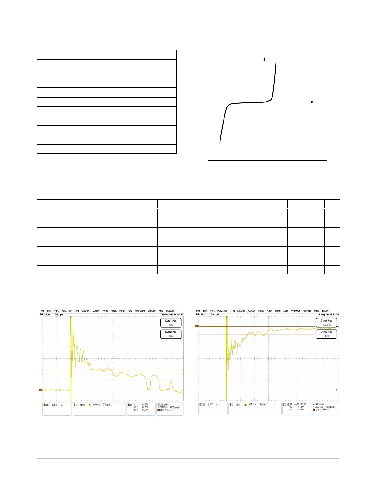
Figure 1. ESD Clamping Voltage Screenshot
Positive 8 kV Contact per IEC61000−4−2
Figure 2. ESD Clamping Voltage Screenshot
Negative 8 kV Contact per IEC61000−4−2
http://onsemi.com
2

2X
PIN ONE
REFERENCE
6X
DETAIL A
0.10 C
2X
0.05 C
0.05 C
6X
L
0.10 C
DETAIL B
D
TOP VIEW
SIDE VIEW
D2
3
1
A1
A
B
E
(A3)
NUP3112UPMU
PACKAGE DIMENSIONS
UDFN6, 1.6x1.6, 0.5P
CASE 517AP−01
ISSUE O
L1
DETAIL A
OPTIONAL
CONSTRUCTION
EXPOSED Cu
A
A1
DETAIL B
CONSTRUCTION
C
SEATING
PLANE
OPTIONAL
L
MOLD CMPD
NOTES:
1. DIMENSIONING AND TOLERANCING PER
ASME Y14.5M, 1994.
2. CONTROLLING DIMENSION: MILLIMETERS.
3. DIMENSION b APPLIES TO PLATED TERMINAL
AND IS MEASURED BETWEEN 0.15 AND
0.30 mm FROM TERMINAL.
4. COPLANARITY APPLIES TO THE EXPOSED
PAD AS WELL AS THE TERMINALS.
MILLIMETERS
DIM MIN MAX
A 0.45 0.55
A1 0.00 0.05
A3 0.13 REF
b 0.20 0.30
D 1.60 BSC
A3
E 1.60 BSC
e 0.50 BSC
D2 1.10 1.30
E2 0.45 0.65
K 0.20 −−−
L 0.20 0.40
L1 0.00 0.15
SOLDERMASK DEFINED
MOUNTING FOOTPRINT*
1.26
E2
K6X
e
BOTTOM VIEW
56
6X
b
0.10 B
NOTE 3
0.05ACC
6X
0.52
0.50 PITCH
1.90
0.61
1
6X
0.32
DIMENSIONS: MILLIMETERS
*For additional information on our Pb−Free strategy and soldering
details, please download the ON Semiconductor Soldering and
Mounting Techniques Reference Manual, SOLDERRM/D.
ON Semiconductor and are registered trademarks of Semiconductor Components Industries, LLC (SCILLC). SCILLC reserves the right to make changes without further notice
to any products herein. SCILLC makes no warranty, representation or guarantee regarding the suitability of its products for any particular purpose, nor does SCILLC assume any liability
arising out of the application or use of any product or circuit, and specifically disclaims any and all liability, including without limitation special, consequential or incidental damages.
“Typical” parameters which may be provided in SCILLC data sheets and/or specifications can and do vary in different applications and actual performance may vary over time. All
operating parameters, including “Typicals” must be validated for each customer application by customer’s technical experts. SCILLC does not convey any license under its patent rights
nor the rights of others. SCILLC products are not designed, intended, or authorized for use as components in systems intended for surgical implant into the body, or other applications
intended to support or sustain life, or for any other application in which the failure of the SCILLC product could create a situation where personal injury or death may occur. Should
Buyer purchase or use SCILLC products for any such unintended or unauthorized application, Buyer shall indemnify and hold SCILLC and its officers, employees, subsidiaries, affiliates,
and distributors harmless against all claims, costs, damages, and expenses, and reasonable attorney fees arising out of, directly or indirectly, any claim of personal injury or death
associated with such unintended or unauthorized use, even if such claim alleges that SCILLC was negligent regarding the design or manufacture of the part. SCILLC is an Equal
Opportunity/Affirmative Action Employer. This literature is subject to all applicable copyright laws and is not for resale in any manner.
PUBLICATION ORDERING INFORMATION
LITERATURE FULFILLMENT:
Literature Distribution Center for ON Semiconductor
P.O. Box 5163, Denver, Colorado 80217 USA
Phone: 303−675−2175 or 800−344−3860 Toll Free USA/Canada
Fax: 303−675−2176 or 800−344−3867 Toll Free USA/Canada
Email: orderlit@onsemi.com
N. American Technical Support: 800−282−9855 Toll Free
USA/Canada
Europe, Middle East and Africa Technical Support:
Phone: 421 33 790 2910
Japan Customer Focus Center
Phone: 81−3−5773−3850
http://onsemi.com
3
ON Semiconductor Website: www.onsemi.com
Order Literature: http://www.onsemi.com/orderlit
For additional information, please contact your local
Sales Representative
NUP3112UPMU/D

 Loading...