

NCP81172
2-Phase Synchronous Buck
Controller with Integrated
Gate Drivers and PWM VID
Interface
The NCP81172, a general−purpose two−phase synchronous buck
controller, integrates gate drivers and PWM VID interface in a
QFN−24 package and provides a compact−footprint power
management solution for new generation computing processors. It
receives power save command (PSI) from processors and operates in
1−phase diode emulation mode to obtain high efficiency in light−load
condition. Operating in high switching frequency up to 800 kHz
allows employing small size inductor and capacitors. The part is able
to support all−ceramic−capacitor applications.
Features
4.5 V to 24 V Input Voltage Range
Output Voltage up to 2.0 V with PWM VID Interface
Differential Output Voltage Sense
Integrated Gate Drivers
200 kHz ~ 800 kHz Switching Frequency
Power Saving Interface (PSI)
Power Good Output
Programmable Over Current Protection
Over Voltage Protection
Under Voltage Protection
Temperature Sense and Alert Output
Thermal Shutdown Protection
QFN−24, 4 x 4 mm, 0.5 mm Pitch Package
This is a Pb−Free Device
Typical Applications
GPU and CPU Power
Graphics Card Applications
Desktop and Notebook Applications
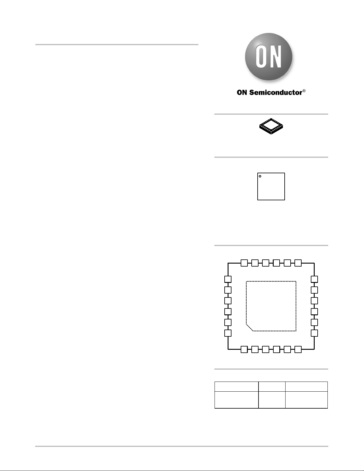
http://onsemi.com
24
1
QFN24
CASE 485L
MARKING DIAGRAM
81172
ALYWG
G
81172 = Specific Device Code
A = Assembly Location
L = Wafer Lot
Y = Year
W = Work Week
G = Pb−Free Package
PINOUT
HG2
BST2
PH219
LG220
PVCC21
PGND22
LG123
PH124
BST1
HG1
PGOOD
25
GND
EN
VCC
PSI
TALERT#
VID
131415161718
TSNS
COMP
FBRTN
VREF
REFIN
VIDBUF
654321
12
11
FB
10
9
FS
8
7
Semiconductor Components Industries, LLC, 2013
April, 2013 − Rev. 1
(Top View)
ORDERING INFORMATION
Device Package Shipping
NCP81172MNTXG QFN24
(Pb−Free)
†For information on tape and reel specifications,
including part orientation and tape sizes, please
refer to our Tape and Reel Packaging Specification
Brochure, BRD8011/D.
1 Publication Order Number:
4000 / Tape &
†
Reel
NCP81172/D
NCP81172
+5 V
+3.3 V
EN
PSI
VID
PG
TALT
15 VCC
25 GND
3
EN
4
PSI
16
PGOOD
14
TALERT#
5
VID
13 TSNS
8 VREF
7 REFIN
NCP81172
21PVCC
22PGND
2HG1
1BST1
24PH1
23LG1
17HG2
18BST2
19PH2
20LG2
10FBRTN
+5 V
VIN
VOUT
VIN
6 VIDBUF
9 FS
11FB
12COMP
Figure 1. Typical Application Circuit with PWM−VID Interface
http://onsemi.com
2
NCP81172
+5 V
+3.3 V
EN
PSI
PG
TALT
15 VCC
25 GND
EN
3
PSI
4
16
PGOOD
14
TALERT#
5
VID
13 TSNS
8 VREF
7 REFIN
NCP81172
21PVCC
22PGND
2HG1
1BST1
24PH1
23LG1
17HG2
18BST2
19PH2
20LG2
10FBRTN
+5 V
VIN
VOUT
VIN
6 VIDBUF
9 FS
11FB
12COMP
Figure 2. Typical Application Circuit without PWM−VID Interface
http://onsemi.com
3
NCP81172
15
3
16
13
14
4
9
8
VCC
EN
PGOOD
TSNS
TALERT#
PSI
FS
VREF
UVLO
&
PGOOD
Thermal
Management
PSI
Control
Ramp
Generator
Reference
Voltage
FAULT
RAMP1
PH1
RAMP2
2/1 Phase
PWM
Control
&
Protections
(OVP, UVP, OCP)
PWM1
PWM2
Gate Drive
1
Gate Drive
2
PVCC
PVCC
PVCC
PVCC
BST1
HG1
PH1
LG1
PGND
BST2
HG2
PH2
LG2
21
1
2
24
23
22
18
17
19
20
5
6
7
11
10
25
12
VID
VIDBUF
REFIN
FB
FBRTN
GND
COMP
CS1
Current
CS2
Figure 3. Functional Block Diagram
Sense
PGND
PWM1
PH1
LG1
PWM2
PH2
LG2
GND
http://onsemi.com
4

NCP81172
PIN DESCRIPTION
Pin Name Type Description
1 BST1 Analog Power Bootstrap 1. Provides bootstrap voltage for the high−side gate drive of phase 1.
2 HG1 Analog Output High−Side Gate 1. Directly connected with the gate of the high−side power MOSFET
3 EN Logic Input Enable. Logic high enables the device and logic low makes the device in standby
4 PSI Logic Input Power Saving Interface. Logic high enables 2 phase CCM operation, mid level
5 VID Logic Input Voltage ID. Voltage ID input from processor.
6 VIDBUF Analog Output Voltage ID Buffer. VID PWM pulse output from an internal buffer.
7 REFIN Analog Input Reference Input. Reference voltage input for output voltage regulation. The pin is
8 VREF Analog Output Output Reference Voltage. Precise 2 V reference voltage output. A 10 nF ceramic
9 FS Analog Input Frequency Selection. A resistor from this pin to ground programs switching frequency.
10 FBRTN Analog Input Voltage Feedback Return Input. An inverting input of internal error amplifier.
11 FB Analog Input Feedback. An inverting input of internal error amplifier.
12 COMP Analog Output Compensation. Output pin of error amplifier.
13 TSNS Analog Input Temperature Sensing. Temperature sensing input.
14 TALERT# Logic Output Thermal Alert. Open drain output and active low indicates over temperature.
15 VCC Analog Power
16 PGOOD Logic Output Power GOOD. Open−drain output. Provides a logic high valid power good output
17 HG2 Analog Output High−Side Gate 2. Connected with the gate of the high−side power MOSFET in
18 BST2 Analog Power Bootstrap 2. Provides bootstrap voltage for the high−side gate drive of phase 2.
19 PH2 Analog Input Phase Node 2. Connected to interconnection between high−side MOSFET and
20 LG2 Analog Output Low−Side Gate 2. Connected with the gate of the low−side power MOSFET in
21 PVCC Analog Power Voltage Supply of Gate Drivers. Power supply input pin of internal gate drivers.
22 PGND Analog Ground Power Ground. Power ground of internal gate drivers. Must be connected to the
23 LG1 Analog Output Low−Side Gate 1. Connected with the gate of the low−side power MOSFET in
24 PH1 Analog Input Phase Node 1. Connected to interconnection between high−side MOSFET and
25 THERM/GND Analog Ground Thermal Pad and Analog Ground. Ground of internal control circuits. Must be
A 0.1 mF ~ 1 mF ceramic capacitor is required from this pin to PH1 (pin 24).
of phase 1.
mode.
enables 1−phase CCM operation, and logic low enables 1−phase CCM/DCM
operation.
connected to a non−inverting input of internal error amplifier.
capacitor is required from this pin to GND.
Voltage Supply of Controller. Power supply input pin of control circuits. A 1 mF or larger
ceramic capacitor bypasses this input to GND. This capacitor should be placed as
close as possible to this pin.
signal, indicating the regulator’s output is in regulation window.
phase 2.
A 0.1 mF ~ 1 mF ceramic capacitor is required from this pin to PH2 (pin 19).
low−side MOSFET in phase 2.
phase 2.
A 4.7 mF or larger ceramic capacitor bypasses this input to ground. This capacitor
should be placed as close as possible to this pin.
system ground.
phase 1.
A resistor may be applied between this pin and GND to program OCP threshold.
low−side MOSFET in phase 1.
connected to the system ground.
http://onsemi.com
5

NCP81172
MAXIMUM RATINGS
Value
Rating Symbol
PH to PGND V
Gate Driver Supply Voltage PVCC to GND V
Supply Voltage VCC to GND V
BST to PGND V
BST to PH V
HG to PH V
LG to GND V
PGND to GND V
FBRTN to GND V
PH
PVCC
VCC
BST_PGND
BST_PH
HG
LG
PGND
FBRTN
Other Pins to GND −0.3 VCC+0.3 V
Human Body Model (HBM) ESD Rating Are (Note 1) ESD HBM 2000 V
Machine Model (MM) ESD Rating Are (Note 1) ESD MM 200 V
Latch up Current: (Note 2)
All pins, except digital pins
I
LU
Digital pins
Operating Junction Temperature Range (Note 4) T
Operating Ambient Temperature Range T
Storage Temperature Range T
Thermal Resistance Junction to Top Case (Note 5)
Thermal Resistance Junction to Board (Note 5)
Thermal Resistance Junction to Ambient (Note 4) R
Power Dissipation (Note 6) P
J
A
STG
R
Ψ
JC
R
Ψ
JB
JA
D
Moisture Sensitivity Level (Note 7) MSL 1 −
Stresses exceeding Maximum Ratings may damage the device. Maximum Ratings are stress ratings only. Functional operation above the
Recommended Operating Conditions is not implied. Extended exposure to stresses above the Recommended Operating Conditions may affect
device reliability.
1. This device is ESD sensitive. Handling precautions are needed to avoid damage or performance degradation.
2. Latch up Current per JEDEC standard: JESD78 class II.
3. The thermal shutdown set to 150C (typical) avoids potential irreversible damage on the device due to power dissipation.
4. EDEC standard JESD 51−7 (1S2P Direct−Attach Method) with 0 LFM.
5. JEDEC standard JESD 51−7 (1S2P Direct−Attach Method) with 0 LFM. For checking junction temperature using external measurement.
6. The maximum power dissipation (PD) is dependent on input voltage, maximum output current and external components selected. T ambient
= 25C, Tjunc_max = 125C, PD = (Tjunc_max−T_amb)/Theta JA
7. Moisture Sensitivity Level (MSL): 1 per IPC/JEDEC standard: J−STD−020A.
MIN MAX
−2
30 V
−8 (<100 ns)
−0.3 6.5 V
−0.3 6.5 V
−0.3 35 V
−0.3 6.5 V
−0.3
BST+0.3 V
−2 (<200 ns)
−0.3
PVCC+0.3 V
−2 (<200 ns)
−0.3 0.3 V
−0.3 0.3 V
−100
−10
100
10
−40 125 C
−40 100 C
−40 150 C
6.0 C/W
7.5 C/W
50 C/W
2.0 W
Unit
mA
ELECTRICAL CHARACTERISTICS
(V
= 12 V, V
IN
referenced to T
Characteristics
SUPPLY VOLTAGE
VIN Supply Voltage
Range
VCC Supply Voltage
Range
8. Guaranteed by design, not tested in production.
= V
VCC
from −40C to 100C. unless other noted)
J
PVCC
= 5 V, V
REFIN
= 1.0 V, V
= 3.3 V, typical values are referenced to TJ = 25C, Min and Max values are
PSI
Test Conditions Symbol Min Typ Max Unit
(Note 8) V
(Note 8) V
IN
CC
4.5 12 24 V
4.5 5 5.5 V
http://onsemi.com
6

NCP81172
ELECTRICAL CHARACTERISTICS (continued)
(V
= 12 V, V
IN
referenced to T
Characteristics UnitMaxTypMinSymbolTest Conditions
SUPPLY VOLTAGE
PVCC Supply Voltage
Range
VCC Under−Voltage
(UVLO) Threshold
VCC OK Threshold VCC rising V
SUPPLY CURRENT
VCC Quiescent Current
VCC Shutdown Current EN low I
PVCC Quiescent Supply
Current
PVCC Shutdown Current EN low I
SWITCHING FREQUENCY SETTING
PS0 Switching Frequency
Range
FS Voltage
VOLTAGE REFERENCE
VREF Reference Voltage
PWM MODULATION
Minimum On Time
Minimum Off Time (Note 8) T
Maximum Duty Cycle (Note 8) D
VOLTAGE ERROR AMPLIFIER
Open−Loop DC Gain
Unity Gain Bandwidth (Note 8) GBW
Slew Rate (Note 8) SR
COMP Voltage Swing
FB, REFIN Bias Current VFB = V
Input Offset Voltage V
REFIN Discharge Switch
ON−Resistance
CURRENT−SENSE AMPLIFIER
Closed−Loop DC Gain
−3dB Gain Bandwidth (Note 8) BW
Input Offset Voltage V
ENABLE
EN High Threshold
EN Low Threshold V
EN Input Bias Current External 1k pull−up to 3.3 V I
8. Guaranteed by design, not tested in production.
= V
VCC
from −40C to 100C. unless other noted)
J
PVCC
= 5 V, V
REFIN
= 1.0 V, V
EN high, no switching, PS0
EN high, no switching, PS1/PS2
EN high, no switching, PS0
EN high, no switching, PS1/PS2
RFS = 39.2 kW
I
COMP
I
COMP
= V
osEA
I
REFIN
= VPH − V
osCS
= 3.3 V, typical values are referenced to TJ = 25C, Min and Max values are
PSI
(Note 8) V
VCC falling V
CCUV−
CCOK
I
sdCC
I
PCC
sdPCC
(Note 8) F
V
I
= 1 mA V
REF
(Note 8) T
VREF
on_min
off_min
(Note 8) GAIN
(source) = 2 mA V
(sink) = 2 mA V
= 1.0 V I
REFIN
− VFB (Note 8) V
REFIN
maxCOMP
minCOMP
osEA
(sink) = 2 mA
GAIN
(Note 8) V
PGND
osCS
V
highEN
lowEN
biasEN
PCC
CC
SW
FS
max
EA
EA
COMP
FB
CA
CA
4.5 5 5.5 V
4.0 4.05 4.2 V
4.2 4.25 4.4 V
−
−
− 30 50
−
−
− − 2.0
9
9
0.35
0.35
15
15
0.6
0.6
mA
mA
mA
mA
mA
mA
200 800 kHz
2.0 V
1.98 2.0 2.02 V
50 ns
250 ns
− 100 − %
80 dB
20 MHz
20
V/ms
3.2 3.4 − V
− 1.05 1.15 V
−400 400 nA
−4 4 mV
6.25
W
−5.5 V/V
10 MHz
−500 − 500 uV
1.6 − − V
− − 0.8 V
− − 1.0
mA
http://onsemi.com
7

NCP81172
ELECTRICAL CHARACTERISTICS (continued)
(V
= 12 V, V
IN
referenced to T
Characteristics UnitMaxTypMinSymbolTest Conditions
POWER SAVE INPUT
PSI High Threshold
PSI Low Threshold Rising
PSI Input Bias Current I
SOFT START AND PGOOD
Vout Startup Delay
Cout Startup Slew Rate 3.0 V/ms
PGOOD Startup Delay Measured from EN to PGOOD assertion 2.0 ms
PGOOD Shutdown Delay Measured from EN to PGOOD de−assertion 125 ns
PGOOD Low Voltage I
PGOOD Leakage Current PGOOD = 5 V I
PROTECTION
Current Limit Threshold
Fast Under Voltage
Protection (FUVP)
Threshold
Faster Under Voltage
Protection (FUVP) Delay
Slow Under Voltage
Protection (SUVP)
Threshold
Slow Under Voltage
Protection (SUVP) Delay
Over Voltage Protection
(OVP) Threshold
Over Voltage Protection
(OVP) Delay
Over Temperature
Protection (OTP)
Threshold
Recovery Temperature
Threshold
Over Temperature
Protection (OTP) Delay
OUTPUT DISCHARGE
Output Discharge
Resistance per Phase
8. Guaranteed by design, not tested in production.
= V
VCC
from −40C to 100C. unless other noted)
J
PVCC
= 5 V, V
REFIN
= 1.0 V, V
Measured from EN to Vout Start up from 0 V 1.15 ms
PGOOD
Measured from PGND to Phx
(R
(1%) is connected from LG1
ILMT
to GND)
Voltage from FB to GND 0.15 0.2 0.25 V
Voltage from COMP to GND 3.0 V
Voltage from FB to GND 1.85 2.0 2.15 V
Measured from PHx to PGND when EN is low (Note 8) R
= 3.3 V, typical values are referenced to TJ = 25C, Min and Max values are
PSI
Rising
Falling
Falling
= 4 mA (sink) V
R
is open
ILMT
R
= 6.98 kW
ILMT
R
= 21.0 kW
ILMT
R
= 35.7 kW
ILMT
R
= 49.9 kW
ILMT
V
highPSI
V
lowPSI
biasPSI
lPGOOD
lkgPGOOD
V
OCTH
2.05
0.5
110 122 134
72 82 92
89 100 111
146 163 180
2.4
2.55
2.2
0.8
0.95 V
0.6
− − 1.0
− − 0.3 V
− −
1.0 mA
OCP is disabled −
(Note 8) 2.0
(Note 8)
(Note 8)
50 us
2.0
(Note 8)
(Note 8)
T
sd
T
rec
140 150 C
125 C
(Note 8) 125 ns
dischrg
2
V
mA
mV
ms
ms
kW
http://onsemi.com
8

NCP81172
ELECTRICAL CHARACTERISTICS (continued)
(V
= 12 V, V
IN
referenced to T
Characteristics UnitMaxTypMinSymbolTest Conditions
TSENSE and ALERT
TALERT# Assert
Threshold
TALERT# De−Assert
Threshold
TALERT# Low Voltage I
TALERT# Leakage
Current
PWM−VID BUFFER
VID Input Threshold
Buffer Output Rise Time T
Buffer Output Fall Time T
Rising and Falling Edge
Delay
Propagation Delay Tpd = T
Propagation Delay Error Tpd = T
INTERNAL HIGH−SIDE GATE DRIVE
Pull−High Drive ON
Resistance
Pull−Low Drive ON
Resistance
HG Propagation Delay
Time
INTERNAL LOW−SIDE GATE DRIVE
Pull−High Drive ON
Resistance
Pull−Low Drive ON
Resistance
LG Propagation Delay
Time
BOOTSTRAP
On Resistance of
Rectifier Switch
Rectifier Switch Leakage
Current
8. Guaranteed by design, not tested in production.
= V
VCC
from −40C to 100C. unless other noted)
J
PVCC
= 5 V, V
REFIN
= 1.0 V, V
Measured at TSNS (Temperature Rising)
Measured at TSNS (Temperature Falling) V
ALERT
TALERT# = 5 V I
T = | Tr − Tf | (Note 8)
V
BST
V
BST
– V
= 5 V, IHG = 2 mA (source)
PH
– V
PH
From LG off to HG on
V
– V
PVCC
V
PVCC
– V
PGND
PGND
From HG off to LG on
V
= 5 V, Id = 2 mA, TA = 25C
PVCC
V
PVCC
= 3.3 V, typical values are referenced to TJ = 25C, Min and Max values are
PSI
V
lowTSNS
highTSNS
= 4 mA (sink) V
=T
pHL
pLH
– T
pHL
(Note 8) T
pLH
= 5 V, IHG = 2 mA (sink)
lowALERT
lkgALERT
R
DRV_HH
R
DRV_HL
T
= 5 V, ILG = 2 mA (source)
= 5 V, ILG = 2 mA (sink)
R
DRV_LH
R
DRV_LL
T
R
= 5 V, EN = 0 V
I
lkgBST
0.99 1.00 1.01 V
− 1.05 − V
− − 0.3 V
− −
1.0 mA
1.4 V
r
f
3 ns
3 ns
T 0.5 ns
T
pd
pd
8 ns
0.5 ns
− 1.5 −
− 1.0 −
pdHG
16 ns
− 1.0 −
− 0.5 −
pdLG
BST
5.0 14 20
10 ns
− − 3
W
W
W
W
W
mA
http://onsemi.com
9

NCP81172
DETAILED DESCRIPTION
General
The NCP81172, a 2−phase synchronous buck controller,
integrates gate drivers and PWM VID interface in a QFN−24
of multi−phase current−mode RPM control results in fast
transient response and good dynamic current balance. It is
able to support all−ceramic−capacitor applications.
package and provides a compact−footprint power
management solution for new generation computing
processors. It receives power save input (PSI) from
processors and operates in 1−phase diode emulation mode
to obtain high efficiency in light−load condition. Operating
in high switching frequency up to 800 kHz allows
Operation Modes
The NCP81172 has three power operation modes
responding to PSI levels as shown in Table 1. The operation
mode can be changed on the fly. In 1−phase operation, no
switching in phase 2.
employing small size inductor and capacitors. Introduction
Table 1. POWER SAVING INTERFACE (PSI) CONFIGURATION
PSI Level Power Mode Phase Configuration
High (PSI 2.4 V) PS0 2−Phase, FCCM
Intermediate (0.8 V < PSI < 2.4 V) PS1 1−Phase, FCCM
Low (PSI 0.8 V) PS2 1−Phase, Auto CCM/DCM
The NCP81172 is also able to support pure single−phase
applications without a need to stuff components for phase 2.
In this configuration, the four pins including BST2, HG2,
LG2, and PH2 can be float, but make sure the voltage at PSI
pin is never in high level.
Switching Frequency
Switching frequency is programmed by a resistor RFS
applied from the FS pin to ground. The typical frequency
range is from 200 kHz to 800 kHz. The FS pin provides
approximately 2 V out and the source current is mirrored
into the internal ramp generator. The switching frequency in
Remote Voltage Sense
2−phase operation (PS0 mode) can be estimated by
A high performance and high input impedance
differential error amplifier, as shown in Figure 4, provides
an accurate sense for the output voltage of the regulator. The
output voltage and FBRTN inputs should be connected to the
regulator’s output voltage sense points via a Kelvin−sense
To reduce output ripple in 1−phase operation, the
switching frequency in PS1 and PS2 modes is set to be
higher than PS0 mode, which can be estimated by
pair. The output voltage sense signal goes through a
compensation network and into the inverting input (FB pin)
of the error amplifier. The non−inverting input of the error
amplifier is connected to the reference input (REFIN pin).
Figure 5 shows a measurement based on a typical
application under condition of V
I
out
mode operation. It can be also found that the higher R
of the low−side MOSFETs the smaller frequency difference
REFIN
7
between PS0 and PS1 mode.
F
SW(kHz)
F
SW(kHz)
+ 6603 @ R
+ 5226 @ R
FS(kW)
FS(kW)
= 20 V, V
in
= 10 A for PS1 mode operation and I
−0.766
−0.665
= 0.9 V,
out
= 20 A for PS0
out
(eq. 1)
(eq. 2)
DS(on)
FB
11
FBRTN
10
GND
25
COMP
12
Figure 4. Differential Error Amplifier
http://onsemi.com
10

NCP81172
Figure 5. Switching Frequency Programmed by Resistor RFS at FS Pin
Soft Start
The NCP81172 has a soft start function. The output starts
to ramp up following a system reset period after the device
is enabled. The device is able to start up smoothly under an
output pre−biased condition without discharging the output
before ramping up.
REFIN Discharge
An internal switch in REFIN pin starts to short REFIN to
GND just after EN is pulled high and it turns off just before
the beginning of the soft start. The typical on resistance of
the switch is 6.25 W.
Output Discharge in Shut Down
The NCP81172 has an output discharge function when the
device is in shutdown mode. The resistors (2 kW per phase)
from PH node to PGND in both phases are active to
discharge the output capacitors.
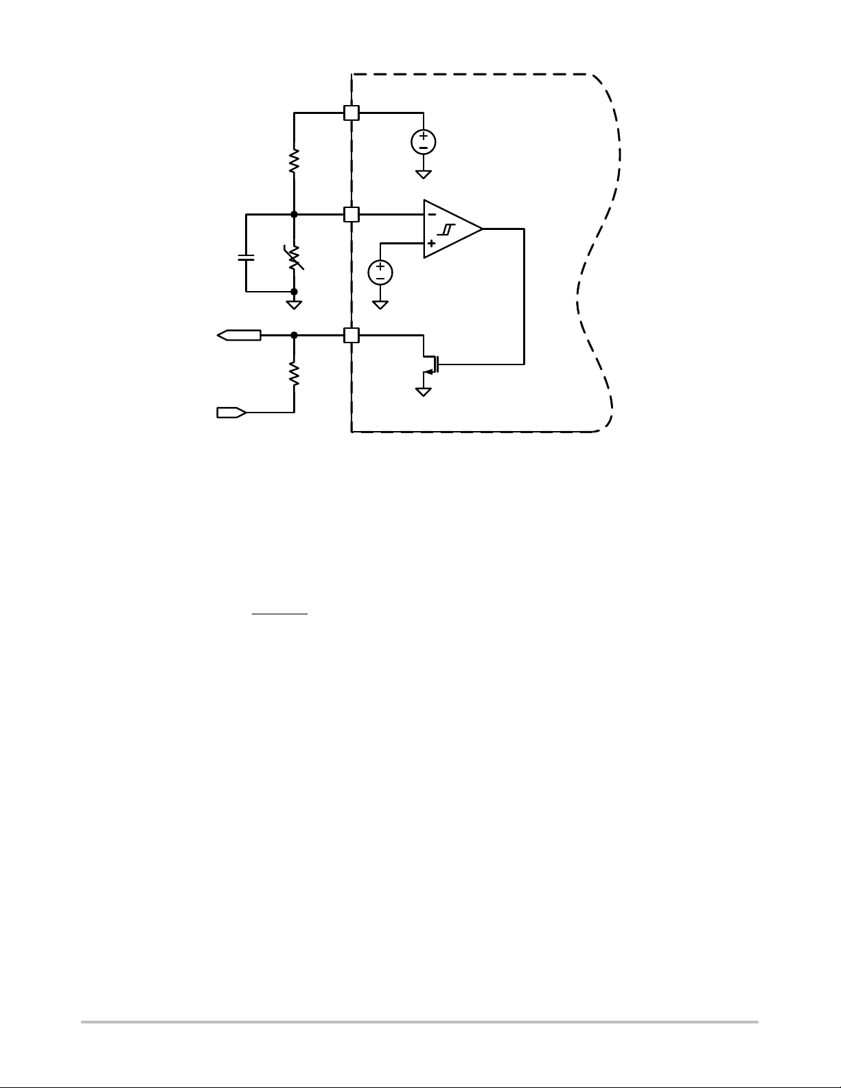
Temperature Sense and Thermal Alert
The NCP81172 provides external temperature sense and
thermal alert in the normal operation mode, and disables the
function in the standby mode. The temperature sense and
thermal alert circuit diagram is shown in . An external
voltage divider, consisting of a NTC thermistor R_NTC and
a resistor R_TSNS, is employed to sense temperature and
program alert level. Usually the thermistor is placed close to
a hot spot like a power MOSFET. The NCP81172 monitors
the voltage at TSNS pin and compares the voltage to an
internal 1 V threshold by an internal comparator. Once the
TSNS voltage drops below 1 V, the comparator turns on an
open−drain switch at TALERT# pin and thus indicates a high
temperature alert. The thermal alert can be de−asserted when
TSNS voltage raises back to be higher than 1.05V. In an
exemplary application where a 100 kW (B = 4250 at 25C)
NTC thermistor is applied together with a 5.62 kW resistor,
an low−valid thermal alert signal is asserted when the
temperature of the NTC thermistor reaches 100C and
de−asserted when the temperature drops down to 97C.
Thermal Shutdown
The NCP81172 has a thermal shutdown protection to
protect the device from overheating when the die
temperature exceeds 150C. Once the thermal protection is
triggered, the fault state can be ended by re−applying VCC
and/or EN if the temperature drops down below 125C.
http://onsemi.com
11
VREF
8
TSNS
13
NCP81172
2.0V
R_NTC R_TSNSR_TALERT
TALERT#
3.3V
14
TALERT#
Figure 6. Temperature Sense and Thermal Alert Circuit Diagram
Over Current Protection
The NCP81172 protects converters from over current.
The current through each phase is monitored by voltage
sensing from phase node PHx to power ground PGND. The
sense signal is compared to an internal voltage threshold.
Once over load happens, the inductor current is limited to an
average current per phase, which can be estimated by
V
+
thOC
R
DS(phase)
(eq. 3)
where R
DS(phase)
I
LMT(phase)
is a total on conduction resistance of
low−side MOSFETs per phase. Normally, a continuous over
load event leads to a voltage drop in the output voltage and
possible to eventually trip under voltage protection.
The over−current threshold can be externally
programmed by adding a 1% tolerance resistor between
LG1 pin and GND. The selectable thresholds can be found
in the electrical table. Please note the maximum RC time
constant formed by the resistor and the total input
capacitance of the low−side MOSFETs should be smaller
than 300 ms in order to make sure the detection voltage
settles well.
Under Voltage Protection
There are two under voltage protections implemented in
the NCP81172, which are fast under voltage protection and
slow under voltage protection.
1.0V
Fast under voltage protection (FUVP) protects converters
in case of an extreme short circuit in output by monitoring
FB voltage. Once FB voltage drops below 0.2 V for more
than 2 ms, the NCP81172 latches off, both the high−side
MOSFETs and the low-side MOSFETs in all phases are
turned off. The fault remains set until the system has either
VCC or EN toggled state. The FUVP function is disabled in
soft start.
Slow under voltage protection (SUVP) of the NCP81172
is based on voltage detection at COMP pin. In normal
operation, COMP level is below 2.5 V. When the output
voltage drops below REFIN voltage for long time and
COMP rises to be over 3 V, an internal UV fault timer will
be triggered. If the fault still exists after 50 ms, the
NCP81172 latches off, both the high-side MOSFETs and the
low−side MOSFETs in all phases are turned off. The fault
remains set until the system has either VCC or EN toggled
state.
Over Voltage Protection
Over voltage protection of the NCP81172 is based on
voltage detection at FB pin. Once FB voltage is over 2 V for
more than 2 ms, all the high−side MOSFETs are turned off
and all the low−side MOSFETs are latched on. The
NCP81172 latches off until the system has either VCC or EN
has toggled state.
http://onsemi.com
12

NCP81172
LAYOUT GUIDELINES
Electrical Layout Considerations
Good electrical layout is a key to make sure proper
operation, high efficiency, and noise reduction.
Power Paths: Use wide and short traces for power paths
to reduce parasitic inductance and high−frequency loop
area. It is also good for efficiency improvement.
Power Supply Decoupling: The power MOSFET
bridges should be well decoupled by input capacitors
and input loop area should be as small as possible to
reduce parasitic inductance, input voltage spike, and
noise emission. Place decoupling caps as close as
possible to the controller VCC and VCCP pins.
Output Decoupling: The output capacitors should be as
close as possible to the load like a GPU. If the load is
distributed, the capacitors should also be distributed
and generally placed in greater proportion where the
load is more dynamic.
Switching Nodes: Switching nodes between HS and LS
MOSFETs should be copper pours to carry high current
and dissipate heat, but compact because they are also
noise sources.
Gate Drive: All the gate drive traces such as HGx, LGx,
PHx, and BSTx should be short, straight as possible,
and not too thin. The bootstrap cap and an option
resistor need to be very close and directly connected
between BSTx pin and PHx pin.
Ground: It would be good to have separated ground
planes for PGND and GND and connect the two planes
at one point. PGND plane is an isolation plane between
noisy power traces and all the sensitive control circuits.
Directly connect the exposed pad (GND pin) to GND
ground plane through vias. The analog control circuits
should be surrounded by GND ground plane. GND
ground plane is connected to PGND plane by single
joint with low impedance.
Voltage Sense: Use Kelvin sense pair and arrange a
“quiet” path for the differential output voltage sense.
Current Sense: The NCP81172 senses phase currents by
monitoring voltages from phase nodes PHx to the
common ground PGND pin. PGND ground plane
should be well underneath PHx trances. To get better
current balance between the two phases, try to make a
layout as symmetrical as possible and balance the
current flow in PGND plane for the two phases.
Temperature Sense: A NTC thermistor is placed close
to a hot spot like a power MOSFET, and a filter
capacitor is placed close to TSNS pin of the controller.
To avoid the traces from/to the NTC thermistor to cross
over other sensitive control circuits.
Compensation Network: The compensation network
should be close to the controller. Keep FB trace short to
minimize their capacitance to GND.
PWM VID Circuit: The PWM VID is a high slew−rate
digital signal from GPU to the controller. The trace
routing of it should be done to avoid noise coupling
from the switching node and to avoid coupling to other
sensitive analog circuit as well. The RC network of the
PWM VID circuit needs to be close to the controller. A
10 nF ceramic cap is connected from VREF pin to
GND plane, and another small ceramic cap is connected
from REFIN pin to GND plane.
Thermal Layout Considerations
Good thermal layout helps high power dissipation from a
small−form factor VR with reduced temperature rise.
The exposed pads of the controller and power
MOSFETs must be well soldered on the board.
A four or more layers PCB board with solid ground
planes is preferred for better heat dissipation.
More vias are welcome to be underneath the exposed
pads and surrounding the power devices to connect the
inner ground layers to reduce thermal resistances.
Use large area copper pour to help thermal conduction
and radiation.
Try distributing multiple heat sources to reduce
temperature rise in hot spots.
http://onsemi.com
13

PIN 1
REFEENCE
2X
0.15 C
2X
0.10 C
0.08 C
NOTE 4
0.15 C
DETAIL A
1
e
e/2
BOTTOM VIEW
D
TOP VIEW
DETAIL B
A3
SIDE VIEW
D2
7
24
NCP81172
PACKAGE DIMENSIONS
QFN24, 4x4, 0.5P
CASE 485L
ISSUE B
A3
NOTES:
1. DIMENSIONING AND TOLERANCING PER ASME
Y14.5M, 1994.
2. CONTROLLING DIMENSION: MILLIMETERS.
3. DIMENSION b APPLIES TO PLATED TERMINAL
AND IS MEASURED BETWEEN 0.25 AND 0.30 MM
FROM THE TERMINAL TIP.
4. COPLANARITY APPLIES TO THE EXPOSED PAD
AS WELL AS THE TERMINALS.
MILLIMETERS
DIM MIN MAX
A 0.80 1.00
A1 0.00 0.05
A3 0.20 REF
b 0.20 0.30
D 4.00 BSC
D2 2.70 2.90
E 4.00 BSC
E2 2.70 2.90
e 0.50 BSC
L 0.30 0.50
L1 0.05 0.15
4.30
2.90
24X
0.55
4.30
A
L
L
B
L1
E
DETAIL A
ALTERNATE
CONSTRUCTIONS
MOLD CMPDEXPOSED Cu
A1
DETAIL B
ALTERNATE TERMINAL
CONSTRUCTIONS
A1
A
SEATING
C
PLANE
RECOMMENDED
24X
L
13
E2
19
b
24X
0.10 B
0.05
C
AC
NOTE 3
SOLDERING FOOTPRINT*
1
2.90
0.50
PITCH
DIMENSIONS: MILLIMETERS
24X
0.32
*For additional information on our Pb−Free strategy and soldering
details, please download the ON Semiconductor Soldering and
Mounting Techniques Reference Manual, SOLDERRM/D.
ON Semiconductor and are registered trademarks of Semiconductor Components Industries, LLC (SCILLC). SCILLC owns the rights to a number of patents, trademarks,
copyrights, trade secrets, and other intellectual property. A listing of SCILLC’s product/patent coverage may be accessed at www.onsemi.com/site/pdf/Patent−Marking.pdf. SCILLC
reserves the right to make changes without further notice to any products herein. SCILLC makes no warranty, representation or guarantee regarding the suitability of its products for any
particular purpose, nor does SCILLC assume any liability arising out of the application or use of any product or circuit, and specifically disclaims any and all liability, including without
limitation special, consequential or incidental damages. “Typical” parameters which may be provided in SCILLC data sheets and/or specifications can and do vary in different applications
and actual performance may vary over time. All operating parameters, including “Typicals” must be validated for each customer application by customer’s technical experts. SCILLC
does not convey any license under its patent rights nor the rights of others. SCILLC products are not designed, intended, or authorized for use as components in systems intended for
surgical implant into the body, or other applications intended to support or sustain life, or for any other application in which the failure of the SCILLC product could create a situation where
personal injury or death may occur. Should Buyer purchase or use SCILLC products for any such unintended or unauthorized application, Buyer shall indemnify and hold SCILLC and
its officers, employees, subsidiaries, affiliates, and distributors harmless against all claims, costs, damages, and expenses, and reasonable attorney fees arising out of, directly or indirectly,
any claim of personal injury or death associated with such unintended or unauthorized use, even if such claim alleges that SCILLC was negligent regarding the design or manufacture
of the part. SCILLC is an Equal Opportunity/Affirmative Action Employer. This literature is subject to all applicable copyright laws and is not for resale in any manner.
PUBLICATION ORDERING INFORMATION
LITERATURE FULFILLMENT:
Literature Distribution Center for ON Semiconductor
P.O. Box 5163, Denver, Colorado 80217 USA
Phone: 303−675−2175 or 800−344−3860 Toll Free USA/Canada
Fax: 303−675−2176 or 800−344−3867 Toll Free USA/Canada
Email: orderlit@onsemi.com
N. American Technical Support: 800−282−9855 Toll Free
USA/Canada
Europe, Middle East and Africa Technical Support:
Phone: 421 33 790 2910
Japan Customer Focus Center
Phone: 81−3−5817−1050
http://onsemi.com
ON Semiconductor Website: www.onsemi.com
Order Literature: http://www.onsemi.com/orderlit
For additional information, please contact your local
Sales Representative
NCP81172/D
14

 Loading...