

NCP6132A, NCP6132B
Dual Output 3 Phase & 2
Phase Controller with
Single SVID Interface for
Desktop and Notebook CPU
Applications
http://onsemi.com
The NCP6132A/NCP6132B dual output three plus two phase buck
solution is optimized for Intel IMVP−7 and VR12 compatible CPUs.
The controller combines true differential voltage sensing, differential
inductor DCR current sensing, input voltage feed−forward, and
adaptive voltage positioning to provide accurately regulated power for
both Desktop and Notebook applications. The control system is based
on Dual−Edge pulse−width modulation (PWM) combined with DCR
current sensing providing the fastest initial response to dynamic load
events and reduced system cost. It also sheds to single phase during
light load operation and can auto frequency scale in light load while
maintaining excellent transient performance.
There are three internal MOSFET drivers inside the chip. One of
these three integrated driver can be configured either to drive core
phase or aux phase. NCP6132A and NCP6132B have almost same
structure except that NCP6132A has two integrated drivers for the
core rail and one integrated driver for auxiliary rail, while the
NCP6132B has all three integrated drivers for the core rail.
Features
• Meets Intel’s VR12/IMVP7 Specifications
• Three Phase CPU Voltage Regulator, and Two Phase Auxiliary
Voltage Regulator, with Three Internal MOSFET Drivers in Total
• Current Mode Dual Edge Modulation for Fastest Initial Response to
Transient Loading
• Dual High Performance Operational Error Amplifier
• One Digital Soft Start Ramp for Both Rails
• Dynamic Reference Injection
• Accurate Total Summing Current Amplifier
• DAC with Droop Feed−forward Injection
• Dual High Impedance Differential Voltage and Total
Current Sense Amplifiers
• Phase−to−Phase Dynamic Current Balancing
• “Lossless” DCR Current Sensing for Current Balancing
• Summed Thermally Compensated Inductor Current
Sensing for Droop
• Power Saving Phase Shedding
• Start Up into Pre−charged Output Voltage
• Adaptive Voltage Positioning (AVP)
• Vin Feed Forward Ramp Slope
• Pin Programming for Internal SVID Parameters
• Over Voltage Protection (OVP) & Under Voltage
Protection (UVP)
• Over Current Protection (OCP)
• Dual Power Good Output with Internal Delays
• Pb−free and Halide−free Packages are Available
• True Differential Current Balancing Sense Amplifiers
for Each Phase
• Switching Frequency Range of 200 kHz − 600 kHz
Applications
• Desktop & Notebook Processors
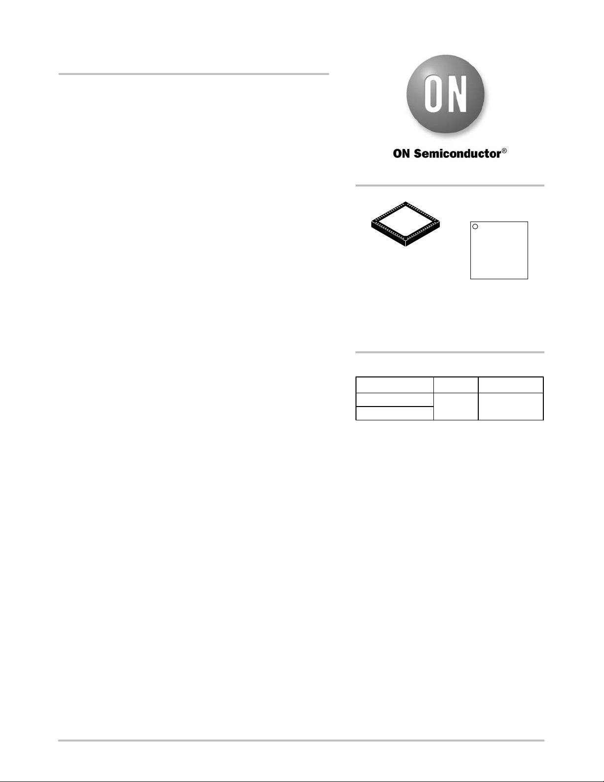
MARKING
DIAGRAM
1
160
QFN60
CASE 485BB
x = A or B
A = Assembly Location
WL = Wafer Lot
YY = Year
WW = Work Week
G = Pb−Free Package
ORDERING INFORMATION
Device Package Shipping
NCP6132AMNR2G
NCP6132BMNR2G
†For information on tape and reel specifications,
including part orientation and tape sizes, please
refer to our Tape and Reel Packaging Specification
Brochure, BRD8011/D.
QFN60
(Pb−Free)
NCP6132x
AWLYYWWG
2500/Tape
& Reel
†
© Semiconductor Components Industries, LLC, 2012
October, 2012 − Rev. 1
1 Publication Order Number:
NCP6132A/D
NCP6132A, NCP6132B
EN
GND
VCC
VDDBP
TSNS
TSNSA
VRHOT#
SDIO
SCLK
ALERT#
VBOOT
VSP
VSN
DROOP
DIFF
COMP
TRBST#
CSSUM
CSREF
CSCOMP
ILIM
IOUT
CSP1
CSP2
CSP3
ENABLE
UVLO & EN
THERMAL
MONITOR
ENABLE
SVID
INTERFACCE
DAC
GND
DIFFAMP
CSREF
1.3 V
FB
ERROR
−
AMP
ENABLE
VSPA
VSNA
DACA
DROOPA
DATA
REGISTERS
TRBST
AUX VR READY
COMPARATOR
DAC
AUX
DAC
VSPA
VSNA
VSP
VSN
ADC
DAC
AUX
DAC
AUX OVP
OVP
ENABLE
MUX
OVPA
OVP
VSP
VSN
DAC
DROOP
VR READY
COMPARATOR
VSPA − VSNA
VSP − VSN
TSNS
TSNSA
IMON
IMONA
IMAX
IMAXA
IOUTA
ILIMA
AUX
DIFFAMP
AUX
CS
AMP
AUX
DAC
GND
CSREFA
1.3 V
−
+
−
VRDYA
VRDY
VSPA
VSNA
DROOPA
DIFFA
CSSUMA
CSREFA
CSCOMPA
ILIMA
IOUTA
FBA
DETECT
CSREF
+
1.3 V
−
+
IOUT
ILIM
MAIN
CURRENT
BALANCE
CS
AMP
ENABLE
CORE PHASE
GENERATOR
COMP
OVP
RAMP1
RAMP2
RAMP3
ENABLE
RAMP
GENERATORS
TRBSTA
DETECT
RAMPA2
RAMPA1
AUX
ERROR
AMP
AUX
PWM
GENERATOR
+
AUX
CURRENT
BALANCE
ENABLE
COMPA
OVPA
1.3 V
COMPA
TRBSTA#
CSP1A
CSP2A
CSREFA
BSTA
HGA
SWA
PVCC
LGA
PVCC
LG1
PGND
BST1
HG1
SW1
PGND
PVCC
LG2
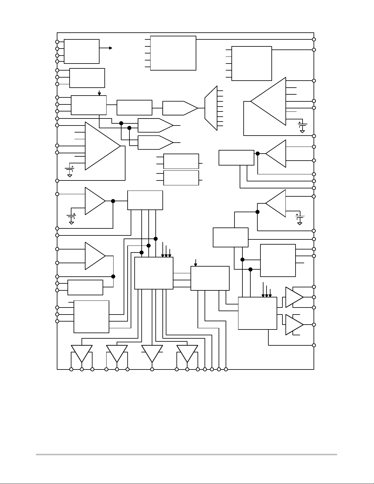
Figure 1. Block Diagram
http://onsemi.com
BST2
PGND
PWMA
HG2
SW2
PWM
VRMP
ROSC
DRVEN
2
VCC
VDDBP
VRDYA
EN
SDIO
ALERT#
SCLK
VBOOT
ROSC
VRMP
VRHOT#
VRDY
VSN
VSP
DIFF
NCP6132A, NCP6132B
FBA
DIFFA
VSNA
VSPA
60
1
15
16
COMPA
TRBSTA#
NCP6132A/NCP6132B
ILIMA
IOUTA
Tab: GND
DROOPA
CSSUMA
CSREFA
CSCOMPA
CSP2A
CSP1A
TSNSA
46
PWMA
45
BSTA
HGA
SWA
LGA
BST2
HG2
SW2
LG2
PVCC
PGND
LG1
SW1
HG1
31
BST1
30
FB
TRBST#
ILIM
IOUT
COMP
DROOP
CSREF
CSSUM
CSCOMP
CSP3
CSP1
CSP2
PWM
TSNS
DRVEN
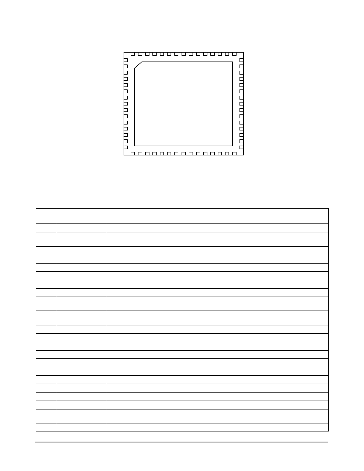
Figure 2. QFN60 Pin Diagram
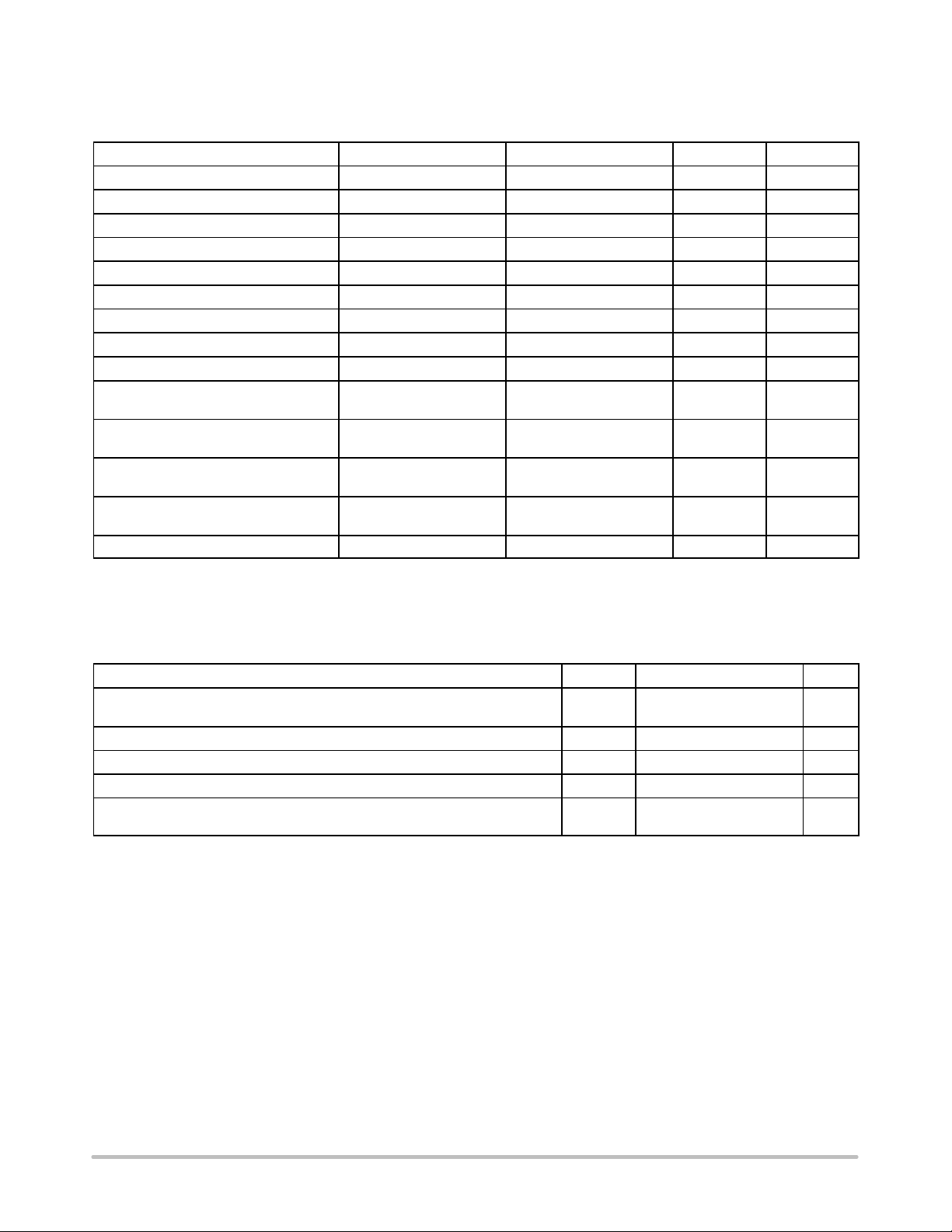
Table 1. QFN60 PIN LIST DESCRIPTION
Pin
No.
1 VCC Power for the internal control circuits. A decoupling capacitor is connected from this pin to ground.
2 VDDBP
3 VRDYA Open drain output. High indicates that the aux output is regulating.
4 EN Logic input. Logic high enables both outputs and logic low disables both outputs.
5 SDIO Serial VID data interface.
6 ALERT# Serial VID ALERT#.
7 SCLK Serial VID clock.
8 VBOOT A resistor to GND on this pin sets the Core and Aux Boot−up Voltage
9 ROSC A resistance from this pin to ground programs the oscillator frequency. This pin supplies a trimmed
10 VRMP Feed−forward input of Vin for the ramp slope compensation. The current fed into this pin is used to
11 VRHOT# Thermal logic output for over temperature.
12 VRDY Open drain output. High indicates that the core output is regulating.
13 VSN Inverting input to the core differential remote sense amplifier.
14 VSP Non−inverting input to the core differential remote sense amplifier.
15 DIFF Output of the core differential remote sense amplifier.
16 TRBST# Compensation pin for the load transient boost.
17 FB Error amplifier voltage feedback for core output
18 COMP Output of the error amplifier and the inverting inputs of the PWM comparators for the core output.
19 IOUT Total output current monitor for core output. Short it to GND if IMON function is not needed.
20 ILIM Over current shutdown threshold setting for core output. Resistor to CSCOMP to set threshold.
21 DROOP Used to program droop function for core output. It’s connected to the resistor divider placed between
22 CSCOMP Output of total current sense amplifier for core output.
Symbol Description
Digital Logic power. Connect this pin to VCC with 10 W. Connect 0.1 mF capacitor from this pin to
ground
output voltage of 2 V.
control of the ramp of PWM slope
CSCOMP and CSREF summing node.
http://onsemi.com
3
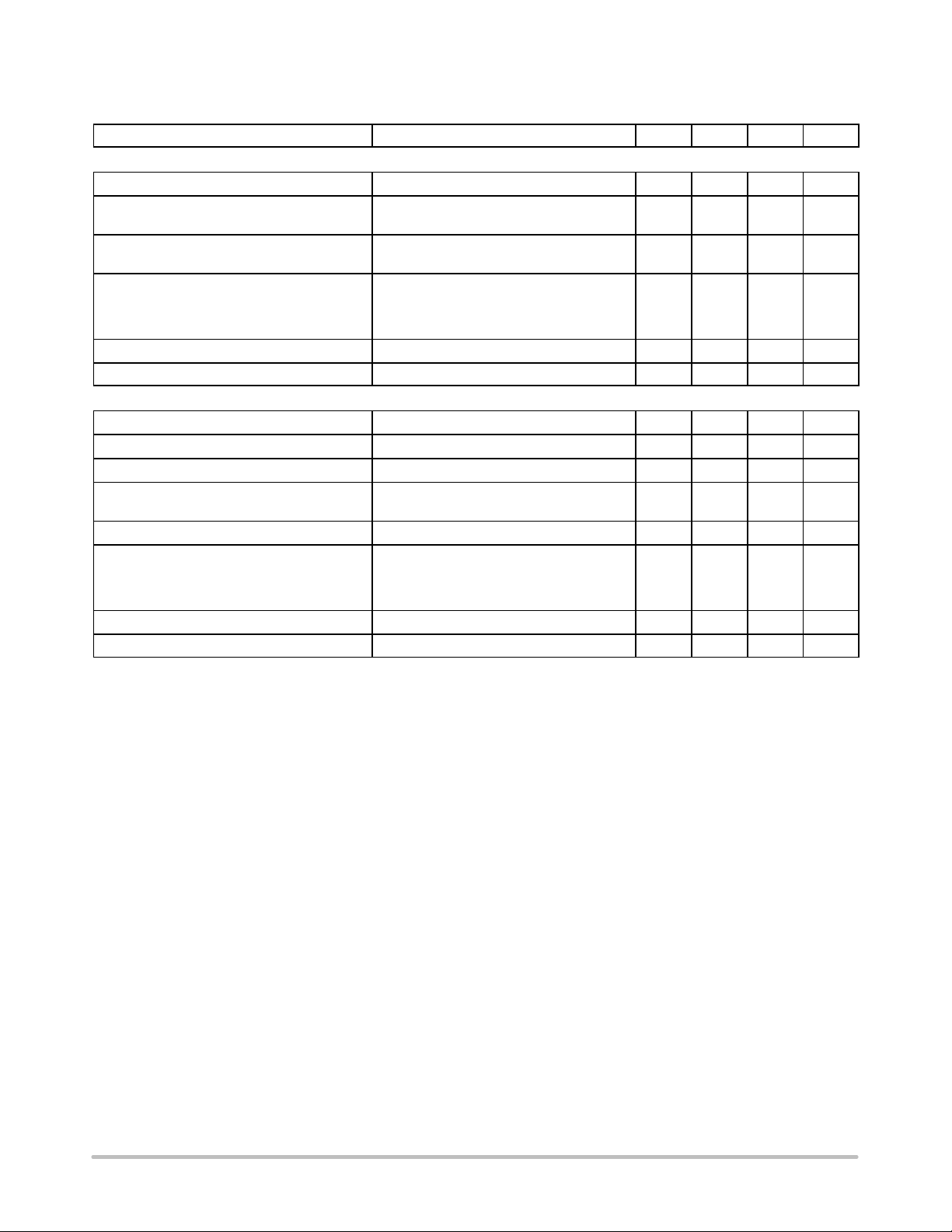
NCP6132A, NCP6132B
Table 1. QFN60 PIN LIST DESCRIPTION
Pin
No.
23 CSSUM Inverting input of total current sense amplifier for core output.
24 CSREF Total output current sense amplifier reference voltage input. And inverting input to core current bal-
ance sense amplifiers.
25 CSP3 Non−inverting input to current balance sense amplifier for phase 3
26 CSP2 Non−inverting input to current balance sense amplifier for phase 2
27 CSP1 Non−inverting input to current balance sense amplifier for phase 1
28 TSNS Temp Sense input for the core converter.
29 DRVEN Bidirectional gate driver enable for external drivers for both core and aux rails. It should be left floating
if unused.
30 PWM Phase 3 PWM output. A resistor to ground on this pin programs IMAX.
31 BST1 High−Side Bootstrap supply for phase 1
32 HG1 High−Side gate drive output for phase 1
33 SW1 Current return for high−side gate drive for phase 1
34 LG1 Low−Side gate drive output for phase 1
35 PGND Power ground for gate drivers
36 PVCC Power Supply for gate drivers
37 LG2 Low−Side gate drive output for phase 2
38 SW2 Current return for high−side gate drive for phase 2
39 HG2 High−Side gate drive output for phase 2
40 BST2 High−Side Bootstrap supply for phase 2
41 LGA Low−Side gate drive output for aux phase 1
42 SWA Current return for high−side gate drive for aux phase 1
43 HGA High−Side gate drive output for aux phase 1
44 BSTA High−Side Bootstrap supply for aux phase 1
45 PWMA Aux Phase 2 PWM output. A resistor to ground on this pin programs IMAXA.
46 TSNSA Temp sense for the aux converter
47 CSP1A Non−inverting input to aux current balance sense amplifier for phase 1
48 CSP2A Non−inverting input to aux current balance sense amplifier for phase 2
49 CSREFA Total output current sense amplifier reference voltage input for aux. Inverting input to aux current
balance sense amplifier for phase 1 and 2
50 CSSUMA Inverting input of total current sense amplifier for aux output
51 CSCOMPA Output of total current sense amplifier for aux output
52 DROOPA Used to program droop function for aux output. It’s connected to the resistor divider placed between
CSCOMPA and CSREFA.
53 ILMA Over current shutdown threshold setting for aux output. Resistor to CSCOMPA to set threshold.
54 IOUTA Total output current monitor for aux output. Short to GND if IMON function is not needed.
55 COMPA Output of aux error amplifier and inverting input of PWM comparator for aux output
56 FBA Error amplifier voltage feedback for aux output
57 TRBSTA# Compensation pin for load transient boost
58 DIFFA Output of the aux differential remote sense amplifier
59 VSPA Non−inverting input to aux differential remote sense amplifier
60 VSNA Inverting input to aux differential remote sense amplifier
61 GND Analog ground
DescriptionSymbol
http://onsemi.com
4
NCP6132A, NCP6132B
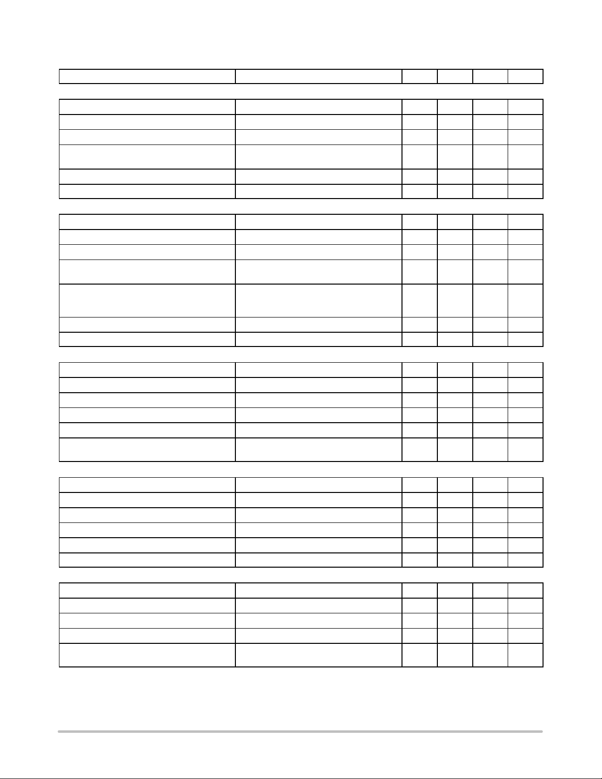
ABSOLUTE MAXIMUM RATINGS
Table 2. ELECTRICAL INFORMATION
Pin Symbol V
MAX
COMP, COMPA VCC + 0.3 V −0.3 V 2 mA 2 mA
CSCOMP, CSCOMPA VCC + 0.3 V −0.3 V 2 mA 2 mA
VSN, VSNA GND + 300 mV GND – 300 mV 1 mA 1 mA
DIFF, DIFFA VCC + 0.3 V −0.3 V 2 mA 2 mA
VRDY, VRDYA VCC + 0.3 V −0.3 V N/A 2 mA
VDDPB, VCC, PVCC 6.5 V −0.3 V N/A N/A
ROSC VCC + 0.3 V −0.3 V 1 mA N/A
IOUT, IOUTA Output TBD −0.3 V
VRMP +25 V −0.3 V
SW1, SW2, SWA 28 V −5 V
BST1, BST2, BSTA 34 V wrt/ GND
6.5 V wrt/ SW
LG1, LG2, LGA VCC + 0.3 V −0.3 V
HG1, HG2, HGA BST + 0.3 V −0.3 V wrt/ SW
−2 V ≤ 200 ns wrt/ SW
All Other Pins VCC + 0.3 V −0.3 V
Stresses exceeding Maximum Ratings may damage the device. Maximum Ratings are stress ratings only. Functional operation above the
Recommended Operating Conditions is not implied. Extended exposure to stresses above the Recommended Operating Conditions may affect
device reliability.
*All signals referenced to GND unless noted otherwise.
V
MIN
−10 V ≤ 200 ns
−0.3 V wrt/ SW
−5 V ≤ 200 ns
I
SOURCE
I
SINK
Table 3. THERMAL INFORMATION
Parameters Symbol Typical Units
Thermal Characteristic
QFN Package (Note 1)
Operating Junction Temperature Range (Note 2) T
Operating Ambient Temperature Range −10 to +100
Maximum Storage Temperature Range T
Moisture Sensitivity Level
QFN Package
*The maximum package power dissipation must be observed.
1. JESD 51−5 (1S2P Direct−Attach Method) with 0 LFM
2. JESD 51−7 (1S2P Direct−Attach Method) with 0 LFM
R
JA
J
STG
−10 to +125
−40 to +150
MSL 1
31
_C/W
_C
_C
_C
http://onsemi.com
5
NCP6132A, NCP6132B
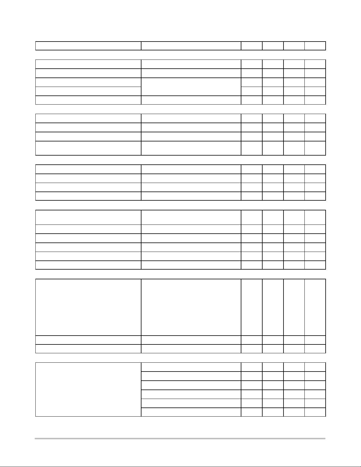
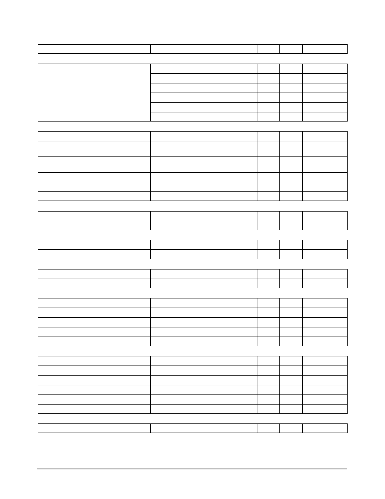
Table 4. NCP6132A/NCP6132B (3+2) ELECTRICAL CHARACTERISTICS
Unless otherwise stated: −10°C < TA < 100°C; VCC = 5.0 V; C
Parameter
ERROR AMPLIFIER
Input Bias Current −400 400 nA
Open Loop DC Gain CL = 20 pF to GND,
Open Loop Unity Gain Bandwidth CL = 20 pF to GND,
Slew Rate
Maximum Output Voltage I
Minimum Output Voltage I
DIFFERENTIAL SUMMING AMPLIFIER
Input Bias Current −400 − 400 nA
VSP Input Voltage Range −0.3 − 3.0 V
VSN Input Voltage Range −0.3 − 0.3 V
−3 dB Bandwidth CL = 20 pF to GND,
Closed Loop DC gain VS to DIFF VS+ to VS− = 0.5 to 1.3 V 1.0 V/V
Droop Accuracy CSREF − DROOP = 80 mV
Maximum Output Voltage I
Minimum Output Voltage I
3. Guaranteed by design/characterization, not in production test
4. Guaranteed by characterization
= 0.1 mF
VCC
Test Conditions Min Typ Max Units
80 dB
RL = 10 kW to GND
55 MHz
RL = 10 kW to GND
DVin = 100 mV, G = −10 V/V,
DV
= 1.5 V – 2.5 V,
out
CL = 20 pF to GND,
20
DC Load = 10k to GND
= 2.0 mA 3.5 − − V
SOURCE
= 2.0 mA − − 1 V
SINK
12 MHz
RL = 10 kW to GND
DAC = 0.8 V to 1.2 V
−10°C ~ 100°C
−10°C ~ 85°C
= 2 mA 3.0 − − V
SOURCE
= 2 mA − − 0.5 V
SINK
78.5
79
81.5
81
V/ms
mV
http://onsemi.com
6
NCP6132A, NCP6132B
Table 5. ELECTRICAL CHARACTERISTICS Unless otherwise stated: −10°C < T
< 100°C; VCC = 5.0 V; C
A
VCC
= 0.1 mF
Parameter Test Conditions Min Typ Max Units
CURRENT SUMMING AMPLIFIER
Offset Voltage (Vos) −300 300
mV
Input Bias Current (CSSUM) CSSUM = CSREF = 1 V −7.5 7.5 nA
Open Loop Gain 80 dB
Current Sense Unity Gain Bandwidth CL = 20 pF to GND,
10 MHz
RL = 10 kW to GND
Maximum CSCOMP (A) Output Voltage I
Minimum CSCOMP(A) Output Voltage
= 2 mA 3.5 − − V
source
I
sink
= 500 mA
− − 0.1 V
CURRENT BALANCE AMPLIFIER
Input Bias Current CSPx = CSREF = 1.2 V −50 − 50 nA
Common Mode Input Voltage Range CSPx = CSREF 0 − 2.0 V
Differential Mode Input Voltage Range CSREF = 1.2 V −100 − 100 mV
Input Offset Voltage Matching CSPx = CSREF = 1.2 V,
−1.5 − 1.5 mV
Measured from the average
Current Sense Amplifier Gain 0 V < CSPx − CSREF < 0.1 V,
−10°C ~ 85°C
−10°C ~ 100°C
5.7
5.5
6.0
6.0
6.3
6.3
V/V
Multiphase Current Sense Gain Matching CSREF = CSP = 10 mV to 30 mV −3 3 %
−3 dB Bandwidth 8 MHz
BIAS SUPPLY
VCC Quiescent Current EN = high 20 27 35 mA
EN = low 10 70
mA
UVLO Threshold VCC rising 4.5 V
VCC falling 4.0 V
VCC UVLO Hysteresis 200 mV
VDDBP Quiescent Current EN = Low
EN = High
0.8
12.0
mA
DAC SLEW RATE
Soft Start Slew Rate 2.33
Slew Rate Slow 3.5
Slew Rate Fast 13.5
AUX Soft Start Slew Rate 2.33
AUX Slew Rate Slow 3.5
AUX Slew Rate Fast 13.5
mv/ms
mv/ms
mv/ms
mv/ms
mv/ms
mv/ms
ENABLE INPUT
Enable High Input Leakage Current External 1k pull−up to 3.3 V − 1.0
Upper Threshold V
Lower Threshold V
Total Hysteresis V
UPPER
UPPER
LOWER
– V
LOWER
Enable Delay Time Measure time from Enable transitioning HI
to when DRON goes high, V
is not 0 V
boot
0.8 V
0.35 V
95 mV
5.0 ms
mA
3. Guaranteed by design/characterization, not in production test
4. Guaranteed by characterization
http://onsemi.com
7
NCP6132A, NCP6132B
Table 5. ELECTRICAL CHARACTERISTICS Unless otherwise stated: −10°C < T
< 100°C; VCC = 5.0 V; C
A
VCC
= 0.1 mF
Parameter UnitsMaxTypMinTest Conditions
DRVEN
Output High Voltage
Output Low Voltage
Rise Time
Fall Time − 2 − ns
Sourcing 500 mA
Sinking 500 mA
CL (PCB) = 20 pF,
DVo = 10% to 90%
Internal Pull Down Resistance EN = Low 70
3.5 V
0.1 V
− 255 − ns
kW
IOUT / IOUTA OUTPUT
Maximum Output Voltage R
Input Referred Offset Voltage I
Output Source Current
Current Gain (IOUT
R
I
limit
CURRENT
= 8.0 kW , Temp range: 0°C to 60°C
OUT
= 5k 2.5 V
lim
to CSREF −2.5 2.5 mV
limit
sink current = 80 mA
) / (ILIM
CURRENT
), R
ILIM
=
9.5 10 10.5
840
mA
OSCILLATOR
Switching Frequency Range 200 − 800 kHz
Switching Frequency Accuracy 200 kHz < Fsw < 800 kHz −10 − 10 %
3 Phase Operation
Rosc Output Voltage
R
osc
R
osc
= 67.4 kW
= 67.4 kW
360 400 440 kHz
1.95 2.00 2.05 V
OUTPUT OVER VOLTAGE & UNDER VOLTAGE PROTECTION (OVP & UVP)
Over Voltage Threshold During Soft−Start &
1.7 1.75 1.8 V
DVID
Over Voltage Threshold Above DAC VSP(A) Rising 225 250 275 mV
Over Voltage Delay VSP(A) rising to PWMx low 50 ns
Under Voltage Threshold Below DAC−DROOP VSP(A) Falling 350 400 450 mV
Under−voltage Hysteresis VSP(A) Rising 25 mV
Under−voltage Delay 5
VR12 DAC
System Voltage Accuracy −105C ~ 855C
1.0 V ≤ DAC < 1.52 V
0.8 V< DAC < 0.995 V
0.5 V < DAC < 0.795 V
0.25 V < DAC < 0.495 V
−0.5
−5
−8
−8
+0.5
+5
+8
+8
mV
mV
mV
−105C ~ 1005C
1.0 V ≤ DAC < 1.52 V
0.8 V< DAC < 0.995 V
0.5 V < DAC < 0.795 V
0.25 V < DAC < 0.495 V
Droop Feed−Forward Current Measure on DROOP pin 60 66 72
1
−12
−12
−12
1
+12
+12
+12
mV
mV
mV
mA
Droop Feed−Forward Pulse On−Time 0.16
OVERCURRENT PROTECTION
ILIM Threshold Current
(OCP shutdown after 50 ms delay)
Aux/Core Multiphase, PS0, R
Aux/Core 1−phase, PS1/2/3, R
Aux 2−phase, PS1, R
Core 2−phase, PS1, R
lim
lim
Aux/Core 2−phase, PS2/3, R
Core 3−phase, PS1/2/3, R
= 20 kW
lim
= 20 kW
lim
= 20 kW
= 20 kW
= 20 kW
lim
= 20 kW
lim
9.0 10 11.0
10
10
6.5
6.5
4.0
mA
mA
mA
mA
mA
mA
3. Guaranteed by design/characterization, not in production test
4. Guaranteed by characterization
ms
%
%
ms
http://onsemi.com
8
NCP6132A, NCP6132B
Table 5. ELECTRICAL CHARACTERISTICS Unless otherwise stated: −10°C < T
< 100°C; VCC = 5.0 V; C
A
VCC
= 0.1 mF
Parameter UnitsMaxTypMinTest Conditions
OVERCURRENT PROTECTION
ILIM Threshold Current
(immediate OCP shutdown)
Aux/Core Multiphase, PS0, R
Aux/Core 1−phase, PS1/2/3, R
Aux 2−phase, PS1, R
Core 2−phase, PS1, R
lim
lim
Aux/Core 2−phase, PS2/3, R
Core 3−phase, PS1/2/3, R
= 20 kW
lim
= 20 kW
lim
= 20 kW
= 20 kW
= 20 kW
lim
= 20 kW
lim
13.5 15 16.5
15
15
10
10
6
mA
mA
mA
mA
mA
mA
MODULATORS (PWM COMPARATORS) FOR CORE & AUX
Minimum Pulse Width Fsw = 350 kHz 60 ns
0% Duty Cycle COMP voltage when the PWM outputs
1.3 − V
remain LO
100% Duty Cycle COMP voltage when the PWM outputs
remain HI V
RMP
= 12.0 V
− 2.5 − V
PWM Ramp Duty Cycle Matching COMP = 2 V, PWM Ton matching −20 20 %
PWM Phase Angle Error Between adjacent phases −25 25 deg
Ramp Feed−forward Voltage range 5 22 V
TRBST#
TRBST/COMP offset TRBST Starts Sinking Current 350 mV
TRBST Sink Capability 500
mA
TRBSTA#
TRBSTA/COMPA offset TRBSTA Starts Sinking Current 350 mV
TRBSTA Sink Capability 500
mA
VRHOT#
Output Low Voltage I_VRHOT = −4 mA 0.3 V
Output Leakage Current High Impedance State −1.0 − 1.0
mA
TSNS/TSNSA
Alert# Assert Threshold 515 mV
Alert# De−assert Threshold 533 mV
VRHOT# Assert Threshold 496 mV
VRHOT# Rising Threshold 515 mV
TSNS Bias Current 115 120 125
mA
ADC
Voltage Range 0 2 V
Total Unadjusted Error (TUE) −1 +1 %
Differential Nonlinearity (DNL) 8−bit 1 LSB
Power Supply Sensitivity +/−1 %
Conversion Time 30
Round Robin 90
ms
ms
VRDY, VRDYA (Power Good) OUTPUT
Output Low Saturation Voltage I
= 4 mA − − 0.3 V
VRDY(A)
3. Guaranteed by design/characterization, not in production test
4. Guaranteed by characterization
http://onsemi.com
9
NCP6132A, NCP6132B
Table 5. ELECTRICAL CHARACTERISTICS Unless otherwise stated: −10°C < T
< 100°C; VCC = 5.0 V; C
A
VCC
= 0.1 mF
Parameter UnitsMaxTypMinTest Conditions
VRDY, VRDYA (Power Good) OUTPUT
Rise Time
Fall Time
Output Voltage at Power−up
External pull−up of 1 kW to 3.3 V,
C
= 45 pF, DVo = 10% to 90%
TOT
External pull−up of 1 kW to 3.3 V,
C
= 45 pF, DVo = 90% to 10%
TOT
VRDY, VRDYA pulled up to 5 V via 2 kW
− 100 ns
10 ns
− − 1.0 V
Output Leakage Current When High VRDY & VRDYA = 5.0 V −1.0 − 1.0
VRDY Delay (rising) DAC = TARGET to VRDY 500
VRDY Delay (falling) From OCP or OVP − 5 −
PWM, PWMA OUTPUTS
Output High Voltage
Sourcing 500 mA
VCC –
− − V
1.0 V
Output Mid Voltage No Load, SetPS = 02 1.3 2.0 2.7 V
Output Low Voltage
Rise and Fall Time
Sinking 500 mA
CL (PCB) = 50 pF, DVo = GND to VCC
− − 0.7 V
− 10 ns
Tri−State Output Leakage Gx = 2.0 V, x = 1−4, EN = Low −1.0 − 1.0
PHASE DETECTION
CSP1A, CSP2A, CSP2, CSP3
4.2 V
Pin Threshold Voltage
SCLK, SDIO
V
V
V
V
R
IL
IH
HYS
OH
ON
Input Low Voltage 0.45 V
Input High Voltage 0.65 V
Hysteresis Voltage 50 mV
Output High Voltage 1.05 V
Buffer On Resistance
4 13
(data line, ALERT#, and VRHOT#)
Leakage Current −100 100
Pad Capacitance (Note 3) 4.0 pF
VR clock to data delay (Tco) (Note 3) 4 8.3 ns
Setup time (Tsu) (Note 3) 7 ns
Hold time (Thld) (Note 3) 14 ns
HIGH−SIDE MOSFET DRIVER
Pull−up Resistance, Sourcing Current (Note 4) BST = PVCC 1.2 2.0
High Side Driver Sourcing Current BST = PVCC 4.17 A
Pull−down Resistance, Sinking Current
BST = PVCC 0.8 2.0
(Note 4)
High Side Driver Sinking Current BST = PVCC 6.25 A
HG1, HG2, HGA Rise Time VCC = 5 V, 3 nF load, BST − SW = 5 V 6 16 30 ns
HG1, HG2, HGA Fall Time VCC = 5 V, 3 nF load, BST − SW = 5 V 6 11 30 ns
HG1, HG2, HGA Turn−On Propagation Delay
tpdh
DRVH
C
= 3 nF 16 40 47 ns
LOAD
SW1, SW2, SWA Pull−Down Resistance SW to PGND 2
HG1, HG2, HGA Pull−Down Resistance HG to SWBST−SW = 0 V 260
3. Guaranteed by design/characterization, not in production test
4. Guaranteed by characterization
mA
ms
ms
mA
W
mA
W
W
kW
kW
http://onsemi.com
10

NCP6132A, NCP6132B
Table 5. ELECTRICAL CHARACTERISTICS Unless otherwise stated: −10°C < T
< 100°C; VCC = 5.0 V; C
A
VCC
= 0.1 mF
Parameter UnitsMaxTypMinTest Conditions
HIGH−SIDE MOSFET DRIVER
BST Quiescent Current EN = L (shutdown)
EN = H, no switching
1.0
300
10
LOW−SIDE MOSFET DRIVER
Pull−up Resistance, Sourcing Current (Note 4) 0.9 2.0
Low Side Driver Sourcing Current 5.56 A
Pull−down Resistance, Sinking Current
0.4 1.0
(Note 4)
Low Side Driver Sinking Current 12.5 A
LG1, LG2, LGA Rise Time 3 nF load 6 16 30 ns
LG1, LG2, LGA Fall Time 3 nF load 6 11 30 ns
LG1, LG2, LGA Turn−On Propagation Delay
tpdh
DRVL
C
= 3 nF 11 30 ns
LOAD
LG1, LG2, LGA Pull−Down Resistance LG to PGND, VCC = 5 V 45
PVCC Quiescent Current EN = L (Shutdown)
EN = H, no switching
1.0
490
10
BOOTSTRAP RECTIFIER SWITCH
On Resistance EN = L or EN = H and DRVL = H 5.0 9.0 14.0
3. Guaranteed by design/characterization, not in production test
4. Guaranteed by characterization
mA
W
W
kW
mA
W
tf
DRVL
DRVL
tpdh
DRVH
tr
DRVH
DRVH
(WITH RESPECT TO SW)
V
TH
SW
Figure 3. Timing Diagram
NOTE: Timing is referenced to the 90% and 10% points, unless otherwise noted.
V
TH
1.0V
tr
tf
DRVL
DRVH
tpdh
DRVL
http://onsemi.com
11

NCP6132A, NCP6132B
Table 6. VR12, IMVP−7 VID CODES
VID7 VID6 VID5 VID4 VID3 VID2 VID1 VID0 Voltage (V) HEX
0 0 0 0 0 0 0 0 OFF 00
0 0 0 0 0 0 0 1 0.25000 01
0 0 0 0 0 0 1 0 0.25500 02
0 0 0 0 0 0 1 1 0.26000 03
0 0 0 0 0 1 0 0 0.26500 04
0 0 0 0 0 1 0 1 0.27000 05
0 0 0 0 0 1 1 0 0.27500 06
0 0 0 0 0 1 1 1 0.28000 07
0 0 0 0 1 0 0 0 0.28500 08
0 0 0 0 1 0 0 1 0.29000 09
0 0 0 0 1 0 1 0 0.29500 0A
0 0 0 0 1 0 1 1 0.30000 0B
0 0 0 0 1 1 0 0 0.30500 0C
0 0 0 0 1 1 0 1 0.31000 0D
0 0 0 0 1 1 1 0 0.31500 0E
0 0 0 0 1 1 1 1 0.32000 0F
0 0 0 1 0 0 0 0 0.32500 10
0 0 0 1 0 0 0 1 0.33000 11
0 0 0 1 0 0 1 0 0.33500 12
0 0 0 1 0 0 1 1 0.34000 13
0 0 0 1 0 1 0 0 0.34500 14
0 0 0 1 0 1 0 1 0.35000 15
0 0 0 1 0 1 1 0 0.35500 16
0 0 0 1 0 1 1 1 0.36000 17
0 0 0 1 1 0 0 0 0.36500 18
0 0 0 1 1 0 0 1 0.37000 19
0 0 0 1 1 0 1 0 0.37500 1A
0 0 0 1 1 0 1 1 0.38000 1B
0 0 0 1 1 1 0 0 0.38500 1C
0 0 0 1 1 1 0 1 0.39000 1D
0 0 0 1 1 1 1 0 0.39500 1E
0 0 0 1 1 1 1 1 0.40000 1F
0 0 1 0 0 0 0 0 0.40500 20
0 0 1 0 0 0 0 1 0.41000 21
0 0 1 0 0 0 1 0 0.41500 22
0 0 1 0 0 0 1 1 0.42000 23
0 0 1 0 0 1 0 0 0.42500 24
0 0 1 0 0 1 0 1 0.43000 25
0 0 1 0 0 1 1 0 0.43500 26
0 0 1 0 0 1 1 1 0.44000 27
0 0 1 0 1 0 0 0 0.44500 28
0 0 1 0 1 0 0 1 0.45000 29
0 0 1 0 1 0 1 0 0.45500 2A
http://onsemi.com
12

NCP6132A, NCP6132B
Table 6. VR12, IMVP−7 VID CODES
VID7 HEXVoltage (V)VID0VID1VID2VID3VID4VID5VID6
0 0 1 0 1 0 1 1 0.46000 2B
0 0 1 0 1 1 0 0 0.46500 2C
0 0 1 0 1 1 0 1 0.47000 2D
0 0 1 0 1 1 1 0 0.47500 2E
0 0 1 0 1 1 1 1 0.48000 2F
0 0 1 1 0 0 0 0 0.48500 30
0 0 1 1 0 0 0 1 0.49000 31
0 0 1 1 0 0 1 0 0.49500 32
0 0 1 1 0 0 1 1 0.50000 33
0 0 1 1 0 1 0 0 0.50500 34
0 0 1 1 0 1 0 1 0.51000 35
0 0 1 1 0 1 1 0 0.51500 36
0 0 1 1 0 1 1 1 0.52000 37
0 0 1 1 1 0 0 0 0.52500 38
0 0 1 1 1 0 0 1 0.53000 39
0 0 1 1 1 0 1 0 0.53500 3A
0 0 1 1 1 0 1 1 0.54000 3B
0 0 1 1 1 1 0 0 0.54500 3C
0 0 1 1 1 1 0 1 0.55000 3D
0 0 1 1 1 1 1 0 0.55500 3E
0 0 1 1 1 1 1 1 0.56000 3F
0 1 0 0 0 0 0 0 0.56500 40
0 1 0 0 0 0 0 1 0.57000 41
0 1 0 0 0 0 1 0 0.57500 42
0 1 0 0 0 0 1 1 0.58000 43
0 1 0 0 0 1 0 0 0.58500 44
0 1 0 0 0 1 0 1 0.59000 45
0 1 0 0 0 1 1 0 0.59500 46
0 1 0 0 0 1 1 1 0.60000 47
0 1 0 0 1 0 0 0 0.60500 48
0 1 0 0 1 0 0 1 0.61000 49
0 1 0 0 1 0 1 0 0.61500 4A
0 1 0 0 1 0 1 1 0.62000 4B
0 1 0 0 1 1 0 0 0.62500 4C
0 1 0 0 1 1 0 1 0.63000 4D
0 1 0 0 1 1 1 0 0.63500 4E
0 1 0 0 1 1 1 1 0.64000 4F
0 1 0 1 0 0 0 0 0.64500 50
0 1 0 1 0 0 0 1 0.65000 51
0 1 0 1 0 0 1 0 0.65500 52
0 1 0 1 0 0 1 1 0.66000 53
0 1 0 1 0 1 0 0 0.66500 54
0 1 0 1 0 1 0 1 0.67000 55
http://onsemi.com
13

NCP6132A, NCP6132B
Table 6. VR12, IMVP−7 VID CODES
VID7 HEXVoltage (V)VID0VID1VID2VID3VID4VID5VID6
0 1 0 1 0 1 1 0 0.67500 56
0 1 0 1 0 1 1 1 0.68000 57
0 1 0 1 1 0 0 0 0.68500 58
0 1 0 1 1 0 0 1 0.69000 59
0 1 0 1 1 0 1 0 0.69500 5A
0 1 0 1 1 0 1 1 0.70000 5B
0 1 0 1 1 1 0 0 0.70500 5C
0 1 0 1 1 1 0 1 0.71000 5D
0 1 0 1 1 1 1 0 0.71500 5E
0 1 0 1 1 1 1 1 0.72000 5F
0 1 1 0 0 0 0 0 0.72500 60
0 1 1 0 0 0 0 1 0.73000 61
0 1 1 0 0 0 1 0 0.73500 62
0 1 1 0 0 0 1 1 0.74000 63
0 1 1 0 0 1 0 0 0.74500 64
0 1 1 0 0 1 0 1 0.75000 65
0 1 1 0 0 1 1 0 0.75500 66
0 1 1 0 0 1 1 1 0.76000 67
0 1 1 0 1 0 0 0 0.76500 68
0 1 1 0 1 0 0 1 0.77000 69
0 1 1 0 1 0 1 0 0.77500 6A
0 1 1 0 1 0 1 1 0.78000 6B
0 1 1 0 1 1 0 0 0.78500 6C
0 1 1 0 1 1 0 1 0.79000 6D
0 1 1 0 1 1 1 0 0.79500 6E
0 1 1 0 1 1 1 1 0.80000 6F
0 1 1 1 0 0 0 0 0.80500 70
0 1 1 1 0 0 0 1 0.81000 71
0 1 1 1 0 0 1 0 0.81500 72
0 1 1 1 0 0 1 1 0.82000 73
0 1 1 1 0 1 0 0 0.82500 74
0 1 1 1 0 1 0 1 0.83000 75
0 1 1 1 0 1 1 0 0.83500 76
0 1 1 1 0 1 1 1 0.84000 77
0 1 1 1 1 0 0 0 0.84500 78
0 1 1 1 1 0 0 1 0.85000 79
0 1 1 1 1 0 1 0 0.85500 7A
0 1 1 1 1 0 1 1 0.86000 7B
0 1 1 1 1 1 0 0 0.86500 7C
0 1 1 1 1 1 0 1 0.87000 7D
0 1 1 1 1 1 1 0 0.87500 7E
0 1 1 1 1 1 1 1 0.88000 7F
1 0 0 0 0 0 0 0 0.88500 80
http://onsemi.com
14

NCP6132A, NCP6132B
Table 6. VR12, IMVP−7 VID CODES
VID7 HEXVoltage (V)VID0VID1VID2VID3VID4VID5VID6
1 0 0 0 0 0 0 1 0.89000 81
1 0 0 0 0 0 1 0 0.89500 82
1 0 0 0 0 0 1 1 0.90000 83
1 0 0 0 0 1 0 0 0.90500 84
1 0 0 0 0 1 0 1 0.91000 85
1 0 0 0 0 1 1 0 0.91500 86
1 0 0 0 0 1 1 1 0.92000 87
1 0 0 0 1 0 0 0 0.92500 88
1 0 0 0 1 0 0 1 0.93000 89
1 0 0 0 1 0 1 0 0.93500 8A
1 0 0 0 1 0 1 1 0.94000 8B
1 0 0 0 1 1 0 0 0.94500 8C
1 0 0 0 1 1 0 1 0.95000 8D
1 0 0 0 1 1 1 0 0.95500 8E
1 0 0 0 1 1 1 1 0.96000 8F
1 0 0 1 0 0 0 0 0.96500 90
1 0 0 1 0 0 0 1 0.97000 91
1 0 0 1 0 0 1 0 0.97500 92
1 0 0 1 0 0 1 1 0.98000 93
1 0 0 1 0 1 0 0 0.98500 94
1 0 0 1 0 1 0 1 0.99000 95
1 0 0 1 0 1 1 0 0.99500 96
1 0 0 1 0 1 1 1 1.00000 97
1 0 0 1 1 0 0 0 1.00500 98
1 0 0 1 1 0 0 1 1.01000 99
1 0 0 1 1 0 1 0 1.01500 9A
1 0 0 1 1 0 1 1 1.02000 9B
1 0 0 1 1 1 0 0 1.02500 9C
1 0 0 1 1 1 0 1 1.03000 9D
1 0 0 1 1 1 1 0 1.03500 9E
1 0 0 1 1 1 1 1 1.04000 9F
1 0 1 0 0 0 0 0 1.04500 A0
1 0 1 0 0 0 0 1 1.05000 A1
1 0 1 0 0 0 1 0 1.05500 A2
1 0 1 0 0 0 1 1 1.06000 A3
1 0 1 0 0 1 0 0 1.06500 A4
1 0 1 0 0 1 0 1 1.07000 A5
1 0 1 0 0 1 1 0 1.07500 A6
1 0 1 0 0 1 1 1 1.08000 A7
1 0 1 0 1 0 0 0 1.08500 A8
1 0 1 0 1 0 0 1 1.09000 A9
1 0 1 0 1 0 1 0 1.09500 AA
1 0 1 0 1 0 1 1 1.10000 AB
http://onsemi.com
15

NCP6132A, NCP6132B
Table 6. VR12, IMVP−7 VID CODES
VID7 HEXVoltage (V)VID0VID1VID2VID3VID4VID5VID6
1 0 1 0 1 1 0 0 1.10500 AC
1 0 1 0 1 1 0 1 1.11000 AD
1 0 1 0 1 1 1 0 1.11500 AE
1 0 1 0 1 1 1 1 1.12000 AF
1 0 1 1 0 0 0 0 1.12500 B0
1 0 1 1 0 0 0 1 1.13000 B1
1 0 1 1 0 0 1 0 1.13500 B2
1 0 1 1 0 0 1 1 1.14000 B3
1 0 1 1 0 1 0 0 1.14500 B4
1 0 1 1 0 1 0 1 1.15000 B5
1 0 1 1 0 1 1 0 1.15500 B6
1 0 1 1 0 1 1 1 1.16000 B7
1 0 1 1 1 0 0 0 1.16500 B8
1 0 1 1 1 0 0 1 1.17000 B9
1 0 1 1 1 0 1 0 1.17500 BA
1 0 1 1 1 0 1 1 1.18000 BB
1 0 1 1 1 1 0 0 1.18500 BC
1 0 1 1 1 1 0 1 1.19000 BD
1 0 1 1 1 1 1 0 1.19500 BE
1 0 1 1 1 1 1 1 1.20000 BF
1 1 0 0 0 0 0 0 1.20500 C0
1 1 0 0 0 0 0 1 1.21000 C1
1 1 0 0 0 0 1 0 1.21500 C2
1 1 0 0 0 0 1 1 1.22000 C3
1 1 0 0 0 1 0 0 1.22500 C4
1 1 0 0 0 1 0 1 1.23000 C5
1 1 0 0 0 1 1 0 1.23500 C6
1 1 0 0 0 1 1 1 1.24000 C7
1 1 0 0 1 0 0 0 1.24500 C8
1 1 0 0 1 0 0 1 1.25000 C9
1 1 0 0 1 0 1 0 1.25500 CA
1 1 0 0 1 0 1 1 1.26000 CB
1 1 0 0 1 1 0 0 1.26500 CC
1 1 0 0 1 1 0 1 1.27000 CD
1 1 0 0 1 1 1 0 1.27500 CE
1 1 0 0 1 1 1 1 1.28000 CF
1 1 0 1 0 0 0 0 1.28500 D0
1 1 0 1 0 0 0 1 1.29000 D1
1 1 0 1 0 0 1 0 1.29500 D2
1 1 0 1 0 0 1 1 1.30000 D3
1 1 0 1 0 1 0 0 1.30500 D4
1 1 0 1 0 1 0 1 1.31000 D5
1 1 0 1 0 1 1 0 1.31500 D6
http://onsemi.com
16

NCP6132A, NCP6132B
Table 6. VR12, IMVP−7 VID CODES
VID7 HEXVoltage (V)VID0VID1VID2VID3VID4VID5VID6
1 1 0 1 0 1 1 1 1.32000 D7
1 1 0 1 1 0 0 0 1.32500 D8
1 1 0 1 1 0 0 1 1.33000 D9
1 1 0 1 1 0 1 0 1.33500 DA
1 1 0 1 1 0 1 1 1.34000 DB
1 1 0 1 1 1 0 0 1.34500 DC
1 1 0 1 1 1 0 1 1.35000 DD
1 1 0 1 1 1 1 0 1.35500 DE
1 1 0 1 1 1 1 1 1.36000 DF
1 1 1 0 0 0 0 0 1.36500 E0
1 1 1 0 0 0 0 1 1.37000 E1
1 1 1 0 0 0 1 0 1.37500 E2
1 1 1 0 0 0 1 1 1.38000 E3
1 1 1 0 0 1 0 0 1.38500 E4
1 1 1 0 0 1 0 1 1.39000 E5
1 1 1 0 0 1 1 0 1.39500 E6
1 1 1 0 0 1 1 1 1.40000 E7
1 1 1 0 1 0 0 0 1.40500 E8
1 1 1 0 1 0 0 1 1.41000 E9
1 1 1 0 1 0 1 0 1.41500 EA
1 1 1 0 1 0 1 1 1.42000 EB
1 1 1 0 1 1 0 0 1.42500 EC
1 1 1 0 1 1 0 1 1.43000 ED
1 1 1 0 1 1 1 0 1.43500 EE
1 1 1 0 1 1 1 1 1.44000 EF
1 1 1 1 0 0 0 0 1.44500 F0
1 1 1 1 0 0 0 1 1.45000 F1
1 1 1 1 0 0 1 0 1.45500 F2
1 1 1 1 0 0 1 1 1.46000 F3
1 1 1 1 0 1 0 0 1.46500 F4
1 1 1 1 0 1 0 1 1.47000 F5
1 1 1 1 0 1 1 0 1.47500 F6
1 1 1 1 0 1 1 1 1.48000 F7
1 1 1 1 1 0 0 0 1.48500 F8
1 1 1 1 1 0 0 1 1.49000 F9
1 1 1 1 1 0 1 0 1.49500 FA
1 1 1 1 1 0 1 1 1.50000 FB
1 1 1 1 1 1 0 0 1.50500 FC
1 1 1 1 1 1 0 1 1.51000 FD
1 1 1 1 1 1 1 0 1.51500 FE
1 1 1 1 1 1 1 1 1.52000 FF
http://onsemi.com
17

12V
5V
EN
SCLK
NCP6132A, NCP6132B
SVID bus idle
SDIO VSPA VID PKT
VSPA
VSP
SVID Alert
VRDYA
VRDY
CPU Driving, Single Data Rate
SCLK
CPU
send
VR latch
SDIO
VSP VID pkt
Figure 4. Start Up Timing Diagram
VR Driving, Single Data Rate
SCLK
VR
send
SDIO
Status PKT
CPU latch
TCO _CPU
T
co_CPU = clock to data delay in CPU
TCO_CPU
thld
tSU
tsu =0.5*T −Tco_CPU
thld =0.5*T +Tco_CPU
TCO_ VR
T
co_VR = clock to data delay in VR
tsu =T −2*Tfly −Tco_VR
thld =2*Tfly +Tco_VR
Tfly propagation time on Serial VID bus
Figure 5. SVID Timing Diagram
http://onsemi.com
18
tSU
thld

NCP6132A, NCP6132B
Table 7. STATE TRUTH TABLE
Error AMP
STATE VRDY(A) Pin
POR
0 < VCC < UVLO
Disabled
EN < threshold
UVLO > threshold
Start up Delay &
Calibration
EN > threshold
UVLO > threshold
DRVEN Fault
EN > threshold
UVLO > threshold
DRVEN < threshold
Soft Start
EN > threshold
UVLO > threshold
DRVEN > High
Normal Operation
EN > threshold
UVLO > threshold
DRVEN > High
Over Voltage Low N/A DAC + 150 mV High
Over Current Low Operational Last DAC Code Low
VID Code = 00h Follows the
N/A N/A N/A Resistive pull down
Low Low Disabled Low
Low Low Disabled Low
Low Low Disabled Resistive pull up Driver must release
Low Operational Active /
High Operational Active /
MultiVR Config
register (34h)
Bit 0 setting
Comp(A) Pin
Low Disabled High, PWM/PWMA
OVP(A) &
UVP(A)
No latch
Latching
DRVEN PIN Method of Reset
DRVEN to high
High
High N/A
Set Valid VID Code
outputs in low state
LGx outputs in high
state
http://onsemi.com
19

NCP6132A, NCP6132B
Controller
POR
VCC < UVLO
OVP
VCC > UVLO
Drive Off
EN = 0
VDRP > ILIM
NO _ CPU
INVALID VID
Soft Start
DAC = Vboot
Soft Start
Disable
EN = 1
Calibrate
3. 5 ms and CAL DONE
Phase
Detect
VCCP > UVLO and DRON HIGH
Ramp
Ramp
VS > OVP
DAC = VID
Normal
VRDY
VS > UVP
VS < UVP
UVP
Figure 6. State Diagram
http://onsemi.com
20

NCP6132A, NCP6132B
General
The NCP6132A/NCP6132B is a dual output three phase plus
two phase dual edge modulated multiphase PWM controller
designed to meet the Intel VR12 and IMVP−7 specifications
with a serial SVID control interface. It is designed to work
in notebook, desktop, and server applications.
User−set Phase and Driver Selection
NCP6132A/NCP6132B can be user−configured to
operate under different phase and driver combinations.
Phase selection for core and aux regulator can be set up
separately by configuring the pin connections of CSP2,
CSP3, CSP1A, and CSP2A. During start−up (before SVID
is available), CSPx pins are monitored to detect user−set
configuration. If a pin is connected to VCC directly or
through a low value (1 kW) resistor, the monitored input
signal is driven to logic high indicating that the
corresponding phase is disabled. Otherwise, if a pin is
connected normally, the monitored input signal is driven to
logic low and that phase is operational. During initialization,
the configuration defined by CSPx is written into a User
Configuration Register (UCR). If the detected configuration
doesn’t match any of the valid configurations listed in the
table below then it is considered as unsupported. With an
unsupported configuration the chip doesn’t start switching
but remains power−up. After initialization the UCR acts as
a Read−Only reg.
The user configuration for core and aux regulator is shown as below:
No Core Rail Aux Rail CSP2 CSP3 CSP1A CSP2A PART
1 2 int. + 1 ext. 1 int. + 1 ext. normal normal Normal normal NCP6132A
2 2 int. + 1 ext. 1 int. normal normal Normal VCC NCP6132A
3 2 int. + 1 ext. off normal normal VCC VCC NCP6132A
4 3 int. 2 ext. normal normal Normal normal NCP6132B
5 3 int. 1 ext. normal normal Normal VCC NCP6132B
6 3 int. off normal normal VCC VCC NCP6132B
7 2 int. 1 int. + 1 ext. normal VCC Normal normal NCP6132A
8 2 int. 1 int. normal VCC Normal VCC NCP6132A
9 2 int. 2 ext. normal VCC Normal normal NCP6132B
10 2 int. 1 ext. normal VCC Normal VCC NCP6132B
11 2 int. off normal VCC VCC VCC NCP6132A or
12 1 int. 1 int. VCC VCC Normal VCC NCP6132A
13 1 int. 1 ext. VCC VCC Normal VCC NCP6132B
14 1 int. off VCC VCC VCC VCC NCP6132A or
*NCP6132A supports configurations: 1, 2, 3, 7, 8, 11, 12 and 14; NCP6132B supports configurations: 4, 5, 6, 9, 10, 11, 13, 14.
*When both CSP1A and CSP2A are pulled to VCC, the aux regulator is totally disabled. It does not respond to any SVID command with address 01h.
NCP6132B
NCP6132B
http://onsemi.com
21

NCP6132A, NCP6132B
If aux rail is disabled, the unused pins’ connection should follow the below table:
UNUSED PIN CONNECTION WITH DISABLED AUX RAIL
Pin Name Connect to
CSP1A V
CSP2A V
LGA Float
SWA Float
HGA Float
BSTA Float
VSPA GND
VSNA GND
DIFFA Float
FBA COMPA
COMPA FBA
TRBSTA# Float or VCC
CSREFA GND
CSCOMPA CSSUMA
CSSUMA CSCOMPA
DROOPA CSCOMPA
ILIMA Float
TSNSA GND
IOUTA GND
PWMA Float
CC
CC
There are three integrated drivers: HG1/LG1, HG2/LG2
and HGA/LGA. There are 5 internal PWM signals:
PWM1/2/3 from core controller and PWM1A/2A from aux
controller. HG1/LG1 is driven by PWM1, HG2/LG2 is
driven by PWM2, and HGA/LGA is driven by PWM1A
when aux rail uses one internal driver, driven by PWM3
when core rail uses 3 internal drivers.
To drive the external drivers, NCP6132A/NCP6132B has
two PWM signal outputs: PWM and PWMA, whose internal
connections depend on the phase and driver configuration.
For example, PWM can be driven by PWM3 when there is
one external driver needed for core rail, or driven by
PWM2A when aux rail requires two external drivers.
Similarly, PWMA can be driven either by PWM1A or
PWM2A. The detailed phase configuration table is shown
below:
PHASE CONFIGURATION TABLE
Aux
1 int. + 1 ext.
Core
2 int. + 1 ext.
Core
3 int.
Core
2 int.
Core
1 int.
Core drivers :
HG1/LG1
HG2/LG2
PWM
Aux drivers :
HGA/LGA
PWMA
No Core drivers :
Core drivers :
HG1/LG1
HG2/LG2
Aux drivers :
HGA/LGA
PWMA
No No Core drivers :
Aux
2 ext.
No Core drivers :
HG1/LG1
HG2/LG2
HGA/LGA
Aux drivers :
PWMA (phase 1)
PWM (phase 2)
Core drivers :
HG1/LG1
HG2/LG2
Aux drivers :
PWMA (phase 1)
PWM (phase 2)
Aux
1 int.
HG1/LG1
HG2/LG2
PWM
Aux drivers :
HGA/LGA
No Core drivers :
Aux drivers :
Core drivers :
HG1/LG1
HG2/LG2
Aux drivers :
HGA/LGA
HG1/LG1
Core drivers :
Aux drivers :
Core drivers :
Aux
1 ext.
No Core drivers :
HG1/LG1
HG2/LG2
HGA/LGA
PWMA
HG1/LG1
HG2/LG2
PWMA
HG1/LG1
HG1/LG1
HG2/LG2
Aux drivers :
Core drivers :
HG1/LG1
HG2/LG2
HGA/LGA
Aux drivers :
Core drivers :
HG1/LG1
HG2/LG2
Aux drivers :
Core drivers :
HG1/LG1
Aux
off
PWM
Aux drivers :
HGA/LGA
http://onsemi.com
22
Aux drivers :
PWMA
Aux drivers :

NCP6132A, NCP6132B
Phase Interleaving
When both core and graphic rails are in multiphase user
configuration, NCP6132A/NCP6132B uses phase
interleaved PWM operation for dual output rails, i.e., there’s
a phase shift between the two rails. The phase shift between
core rail and aux rail is to ensure PWM on−cycle of each
Core
Phase 1
0
˚
Aux
Phase 2
270
Core
Phase 3
240
˚
3+2
˚
Aux
Phase 1
90
Core
Phase 2
120
˚
˚
interleaved phase has no overlap. It helps reduce the RMS
current of the input capacitor connected to Vin and therefore
lower power dissipation over capacitor ESR.
The interleaved phase angle for different phase
configurations is shown in the following diagram.
Core
Phase 1
˚
0
Aux
Phase 2
270
˚
2+2
Core
Phase 2
180
˚
Aux
Phase 1
90
˚
Figure 7. Interleaved Phases Diagram
Phase Shedding (PS)
The NCP6132A/NCP6132B supports phase shedding
based by CPU/GPU PSx states. (Auto Phase Shedding
triggered by user−set phase shedding threshold without any
PS state transition is not supported.) The NCP6132A/
NCP6132B implements PS0, PS1, PS2 and PS3 power
saving states for CPU/GPU shown as follows:
For CPU (3−phase or 2−phase user configuration):
Power Status Phases Operating Mode Control Method
PS0 Heavy load condition Multi−phase interleaving CF DEPWM
PS1 Medium load condition Single−phase Forced CCM mode QCF RPM
PS2/3 Light load condition Single−phase Automatic CCM/DCM mode VF RPM
For GPU (2−phase user configuration):
Power Status Phases Operating Mode Control Method
PS0 Heavy load condition 2−phase interleaving CF DEPWM
PS1 Medium load condition 2−phase interleaving CF DEPWM
PS2/3 Light load condition Single−phase Automatic CCM/DCM mode VF RPM
For CPU & GPU (1−phase user configuration):
Power Status Phases Operating Mode Control Method
PS0 Heavy load condition Single−phase Forced CCM mode QCF RPM
PS1 Medium load condition Single−phase Forced CCM mode QCF RPM
PS2/3 Light load condition Single−phase Automatic CCM/DCM mode VF RPM
*CF – Constant Frequency
DEPWM − Dual Edge Pulse Width Modulation
QCF − Quasi Constant Frequency
RPM – Ramp Pulse Modulation
VF – Variable Frequency
http://onsemi.com
23

NCP6132A, NCP6132B
In PS2/3 state, transition from CCM to DCM is triggered
by a Zero Current Detector (ZCD) latch. ZCD latch is set by
a ZCD comparator monitoring switch node (SWN) voltage
during PWM off−time. ZCD latch is reset at negative edge
of PWM signal and is ready to be set after a set minimum
PWM off−time delay. As SWN voltage is stably ramping up
toward zero, if the SWN voltage crosses a set (a few negative
mV) threshold, then ZCD latch is set and LG1 output is
driven to logic low to turn off low−side power switch and
phase is operating in DCM. If ZCD latch remains reset
during PWM off−cycle, then the low−side power switch
remains turned on and the phase is operating in CCM.
If aux phase 1 is configured with external driver, the driver
should have built−in ZCD comparator (like NCP5911) to
support DCM.
Transition from PS1 to PS0 state triggering phase
shedding is called PS1 assertion. Similarly, PS2 assertion is
the transition to PS2 state. Note that PS1 assertion in aux rail
should be ignored as PS1 and PS0 have the same phase
operating mode.
PS1 or PS2 assertion is ignored and user−set multiphase
operation is enforced for the following circumstances:
during startup, in current limit (CLIMx) operation, and
during DVID transition.
Phase shedding is always from multiphase to single phase
in one single step.
• For core rail:
♦ Phase shedding from 3−phase is done by driving
PWM output (internally connected to PWM3) to
mid−level while DRVEN output is still driven to
logic high, and by keeping both HG2, LG2 outputs
to logic low.
♦ Phase shedding from 2−phase is done by driving
both HG2, LG2 outputs to logic low.
• For aux rail:
♦ Phase shedding from 2−phase is done by driving
both HGA, LGA outputs to logic low.
Transition from PS1/2/3 to PS0 state triggers phase
un−shedding.
Phase un−shedding is instantaneous and happens from
single−phase to user−set multiphase configuration in one
single step.
Serial VID
The NCP6132A/NCP6132B supports the Intel serial VID
interface. It communicates with the microprocessor through
three wires (SCLK, SDIO, ALERT#). The table of
supported registers is shown below.
Index Name Description Access Default
00h Vendor ID Uniquely identifies the VR vendor. The vendor ID assigned by Intel to
01h Product ID Uniquely identifies the VR product. The VR vendor assigns this number. R 0x00
02h Product
Revision
05h Protocol ID Identifies the SVID Protocol the NCP6132A/NCP6132B supports R 0x01
06h Capability Informs the Master of the NCP6132A/NCP6132B’s Capabilities,
10h Status_1 Data register read after the ALERT# signal is asserted. Conveying the status
11h Status_2 Data register showing optional status_2 data. R 00h
12h Temp zone Data register showing temperature zones the system is operating in R 00h
15h I_out 8 bit binary word ADC of current. This register reads 0xFF when the IOUT(A)
16h V_out 8 bit binary word ADC of output voltage, measured between VSP and VSN.
17h VR_Temp 8 bit binary word ADC of voltage. Binary format in deg C, IE 100C = 64h. A
ON Semiconductor is 0x1Ah
Uniquely identifies the revision or stepping of the VR control IC. The VR
vendor assigns this data.
1 = supported, 0 = not supported
Bit 7 = Iout_format. Bit 7 = 0 when 1A = 1LSB of Reg 15h. Bit 7 = 1 when
Reg 15 FFh = Icc_Max. Default = 1
Bit 6 = ADC Measurement of Temp Supported = 1
Bit 5 = ADC Measurement of Pin Supported = 0
Bit 4 = ADC Measurement of Vin Supported = 0
Bit 3 = ADC Measurement of Iin Supported = 0
Bit 2 = ADC Measurement of P
Bit 1 = ADC Measurement of V
Bit 0 = ADC Measurement of I
of the VR.
pin voltage is 2 V. The IOUT(A) voltage should be scaled with an external
resister to ground such that a load equal to Icc_Max generates a 2 V signal.
LSB size is 8 mV
value of 00h indicates this function is not supported
Supported = 1
out
Supported = 1
out
Supported = 1
out
R 0x1Ah
R 0x03
R 0xC7
R 00h
R 01h
R 01h
R 01h
http://onsemi.com
24

NCP6132A, NCP6132B
Index DefaultAccessDescriptionName
18h P_out 8 bit binary word representative of output power. The output voltage is
1Ch Status 2 Last
read
21h Icc_Max Data register containing the Icc_Max the platform supports. The value is
22h Temp_Max Data register containing the max temperature the platform supports and the
24h SR_fast
25h SR_slow Slew Rate for SetVID_slow commands. It is 4X slower than the SR_fast rate.
26h Vboot The NCP6132A/NCP6132B will ramp to Vboot and hold at Vboot until it
30h Vout_Max Programmed by master and sets the maximum VID the VR will support. If a
31h VID setting Data register containing currently programmed VID voltage. VID data format. RW 00h
32h Pwr State Register containing the current programmed power state. RW 00h
33h Offset Sets offset in VID steps added to the VID setting for voltage margining. Bit 7
34h MultiVR Config
multiplied by the output current value and the result is stored in this register. A
value of 00h indicates this function is not supported
When the status 2 register is read its contents are copied into this register.
The format is the same as the Status 2 Register.
measured on the ICCMAX pin on power up and placed in this register. From
that point on the register is read only.
level VR_hot asserts. This value defaults to 100°C and programmable over
the SVID Interface
Slew Rate for SetVID_fast commands. Binary format in mV/ms.
Binary format in mV/ms
receives a new SVID SetVID command to move to a different voltage. Default
value = 0 V.
higher VID code is received, the VR should respond with “not supported”
acknowledge. VR 12 VID format.
is sign bit, 0 = positive margin, 1 = negative margin. Remaining 7 BITS are #
VID steps for margin 2s complement.
00h = no margin
01h = +1 VID step
02h = +2 VID steps
FFh = −1 VID step
FEh = −2 VID steps.
R 01h
R 00h
R 00h
R/W 64h
R 0Ah
R 02h
R 00h
RW FBh
RW 00h
For NCP6132A/NCP6132B, VID code change is supported by SVID interface with three options as below:
SVID Command
Option
SetVID_Fast 01h
SetVID_Slow 02h =1/4 of SetVID_Fast VID code
SetVID_Decay 03h No slew rate control, VID code
Code
Feature
>10 mV/ms VID code change
slew rate
change slew rate
down
Boot Voltage Programming
The NCP6132A/NCP6132B has a VBOOT voltage
register that can be externally programmed for both core and
aux boot−up output voltage. The VBOOT voltage can be
programmed with a resistor from VBOOT pin to GND, or it
can be set to 1.1 V by connecting VBOOT pin to GND to
facilitate mass production. See the Boot Voltage Table.
(Indicating the slew rate of VID code change)
BOOT VOLTAGE TABLE
Boot Voltage (V)
0 10k
0.9 20k
1.0 30k
1.1 40k
1.2 50k
1.35 60k
Register Address
24h
25h
N/A
Resistor Value (W)
Or connect VBOOT pin to GND
Or connect VBOOT pin to V
CC
http://onsemi.com
25

NCP6132A, NCP6132B
SVID Addressing
The NCP6132A/NCP6132B has fixed SVID device
addresses for core and aux rail. The core rail address is 0000,
and aux rail address is 0001.
Remote Sense Amplifier
A high performance high input impedance true
differential amplifier is provided to accurately sense the
output voltage of the regulator. The VSP and VSN inputs
should be connected to the regulator’s output voltage sense
points. The remote sense amplifier takes the difference of
the output voltage with the DAC voltage and adds the droop
voltage to
V
DIFF
+ǒV
)ǒV
VSP
DROOP
* V
VSN
* V
Ǔ)ǒ
CSREF
1.3 V * V
Ǔ
DAC
Ǔ
(eq. 1)
This signal then goes through a standard error
compensation network and into the inverting input of the
error amplifier. The non−inverting input of the error
amplifier is connected to the same 1.3 V reference used for
the differential sense amplifier output bias.
High Performance Voltage Error Amplifier
A high performance error amplifier is provided for high
bandwidth transient performance. A standard type 3
compensation circuit is normally used to compensate the
system.
Differential Current Feedback Amplifiers
Each phase has a low offset differential amplifier to sense
that phase current for current balance and per phase OCP
protection during soft−start. The inputs to the CSREF and
CSPx pins are high impedance inputs. It is recommended
that any external filter resistor RCSN not exceed 10 kW to
avoid offset issues with leakage current. It is also
recommended that the voltage sense element be no less than
0.5 mW for accurate current balance. Fine tuning of this time
constant is generally not required.
L
+
C
CSN
SWNx
PHASE
*DCR
RCSN
DCR
Figure 8.
CSPx
CCSN
LPHASE
12
CSREF
VOUT
R
CSN
The individual phase current is summed into to the PWM
comparator feedback in this way current is balanced is via
a current mode control approach.
Total Current Sense Amplifier
The NCP6132A/NCP6132B uses a patented approach to
sum the phase currents into a single temperature
compensated total current signal. This signal is then used to
generate the output voltage droop, total current limit, and the
output current monitoring functions. The total current signal
is floating with respect to CSREF. The current signal is the
difference between CSCOMP and CSREF. The Ref(n)
resistors sum the signals from the output side of the
inductors to create a low impedance virtual ground. The
amplifier actively filters and gains up the voltage applied
across the inductors to recover the voltage drop across the
inductor series resistance (DCR). Rth is placed near an
inductor to sense the temperature of the inductor. This
allows the filter time constant and gain to be a function of the
Rth NTC resistor and compensate for the change in the DCR
with temperature.
CSN1
CSN2
CSN3
SWN1
SWN2
SWN3
Rref1
Rref2
Rref3
Rph1
Rph2
Rph3
Cref
1n
CSREF
CSSUM
Figure 9.
+
-
CSCOMP
Ccs1
Ccs2
Rcs1Rcs2
Rth
The DC gain equation for the current sensing:
Rcs1*Rth
Rcs1)Rth
Rph
*DCR
Total
(eq. 2)
Ǔ
V
CSCOMP−CSREF
Rcs2 )
+
*ǒIout
Set the gain by adjusting the value of the Rph resistors.
The DC gain should set to the output voltage droop. If the
voltage from CSCOMP to CSREF is less than 100 mV at
ICCMAX then it is recommended to increase the gain of the
CSCOMP amp and add a resister divider to the Droop pin
filter. This is required to provide a good current signal to
offset voltage ratio for the ILIM pin. When no droop is
needed, the gain of the amplifier should be set to provide
~100 mV across the current limit programming resistor at
full load. The values of Rcs1 and Rcs2 are set based on the
220k NTC and the temperature effect of the inductor and
should not need to be changed. The NTC should be placed
near the closest inductor. The output voltage droop should
be set with the droop filter divider.
The pole frequency in the CSCOMP filter should be set
equal to the zero from the output inductor. This allows the
circuit to recover the inductor DCR voltage drop current
http://onsemi.com
26

NCP6132A, NCP6132B
signal. Ccs1 and Ccs2 are in parallel to allow for fine tuning
of the time constant using commonly available values. It is
best to fine tune this filter during transient testing.
DCR@25° C
FZ+
2*PI*L
FP+
ǒ
2 * PI *
Programming the Current Limit
Rcs2 )
Rcs1*Rth@25° C
Rcs1)Rth@25° C
Phase
1
Ǔ
*(Ccs1 ) Ccs
(eq. 3)
(eq. 4)
The current−limit thresholds are programmed with a
resistor between the ILIM and CSCOMP pins. The ILIM pin
mirrors the voltage at the CSREF pin and mirrors the sink
current internally to IOUT (reduced by the IOUT Current
Gain) and the current limit comparators. Set the value of the
current limit resistor based on the user−set output current
limit Iout
or CSREF− CSCOMP voltage at Iout
LIMIT
LIMIT
condition as shown below:
Rcs1*Rth
Rcs2 )
R
+
ILIM
Rcs1)Rth
Rph
10 mA
*ǒIout
LIMIT
* DCR
Ǔ
(eq. 5)
If the Droop at maximum load is less than 100 mV at
ICCMAX we recommend altering this filter into a voltage
divider such that a larger signal can be provided to the ILIM
resistor by increasing the CSCOMP amp gain for better
current monitor accuracy. The DROOP pin divider gain
should be set to provide a voltage from DROOP to CSREF
equal to the amount of voltage droop desired in the output.
A current is applied to the DROOP pin during dynamic VID.
In this case Rdroop1 in parallel with Rdroop2 should be
equal to Rdroop.
Rdroop2
Cdroop
CSREF
CSSUM
5
6
DROOP
+
−
Figure 11.
7
Rdroop1
CSCOMP
or
V
R
ILIM
Programming DROOP and DAC Feed−Forward Filter
CSREF−CSCOMP@ILIMIT
+
10 mA
(eq. 6)
The signals DROOP and CSREF are differentially
summed with the output voltage feedback to add precision
voltage droop to the output voltage. The total current
feedback should be filtered before it is applied to the
DROOP pin. This filter impedance provides DAC
feed−forward during dynamic VID changes. Programming
this filter can be made simpler if CSCOMP−CSREF is equal
to the droop voltage. Rdroop sets the gain of the DAC
feed−forward and Cdroop provides the time constant to
cancel the time constant of the system per the following
equations. Cout is the total output capacitance and Rout is
the output impedance of the system.
Cdroop
CSREF
CSSUM
5
6
Rdroop + Cout * Rout * 453.6x10
Cdroop +
DROOP
+
−
Rout * Cout
Rdroop
Figure 10.
7
Rdroop
CSCOMP
6
Programming IOUT
The IOUT pin sources a current equal to the ILIM sink
current gained by the IOUT Current Gain. The voltage on
the IOUT pin is monitored by the internal A/D converter and
should be scaled with an external resistor to ground such that
a load equal to ICCMAX generates a 2 V signal on IOUT. A
pull−up resistor from 5 V VCC can be used to offset the
IOUT signal positive if needed.
R
+
IOUT
Programming ICC_MAX and ICC_MAXA
Rcs2)
10 *
2.0 V * R
Rcs1*Rth
Rcs1)Rth
Rph
LIMIT
*ǒIout
ICC_MAX
*DCR
(eq. 7)
Ǔ
The SVID interface provides the platform ICC_MAX
value at register 21h for both the core and the aux rails. A
resistor to ground on the PWM and PWMA pins program
these registers at the time the part in enabled. 10 mA is
sourced from these pins to generate a voltage on the program
resistor. The value of the register is 1 A per LSB. When
ICC_MAX is less than 118 A, resistor value is set according
to the equation below. The resistor value should be no less
than 10 k.
R
ICC_MAX
Programming TSNS and TSNSA
ICC_MAX
+
10 mA * 256 A
21h
2V
) 3.5 kW
(eq. 8)
Two temperature sense inputs are provided. A precision
current is sourced out the output of the TSNS and TSNSA
http://onsemi.com
27

NCP6132A, NCP6132B
pins to generate a voltage on the temperature sense network.
The voltages on the temperature sense inputs are sampled by
the internal A/D converter and then digitally converted to
temperature and stored in SVID register 17h. A 100 k NTC
should be used. The Rcomp1 and Rcomp2 vary with NTC’s
temperature characteristics.
TSNS
Rcomp1
0.0
Cfilter
0.1 mF
Rcomp2
8.25K
AGND
Figure 12.
Precision Oscillator
RNTC
100K
AGND
A programmable precision oscillator is provided. The
clock oscillator serves as the master clock to the ramp
generator circuit. This oscillator is programmed by a resistor
to ground on the ROSC pin. The ROSC pin provides
approximately 2 V out and the source current is mirrored
into the internal ramp oscillator. The oscillator generates
triangle ramps that are 0.5 ~ 2.5 V in amplitude depending
on the VRMP pin voltage to provide input voltage feed
forward compensation. The oscillator frequency is
approximately proportional to the current flowing in the
ROSC resistor.
f
OSC
+
V
OSC
ǒ
2
V
ref
1
R
OSCCOSC
) 2t
(eq. 9)
Ǔ
d
Where
f
OSC
V
OSC
PWM master oscillator frequency
oscillator ramp peak−to−peak voltage
(1 V)
V
ref
R
ROSC pin frequency setting resistor
OSC
C
OSC
ROSC pin reference voltage (2 V)
oscillator timing capacitor (2.5 pF)
td oscillator loop delay (10 ns)
And the per phase switching frequency fsw is given by
f
fsw+
OSC
12
(eq. 10)
The switching frequency range is between 200 kHz/phase to
800 kHz/phase.
Programming the Ramp Feed−Forward Circuit
The ramp generator circuit provides the ramp used by the
PWM comparators. The ramp generator provides voltage
feed−forward control by varying the ramp magnitude with
respect to the VRMP pin voltage. The VRMP pin also has
a 4 V UVLO function. The VRMP UVLO is only active
after the controller is enabled. The VRMP pin is a high
impedance input when the controller is disabled.
The PWM ramp time is changed according to the following,
V
RAMPpk+pk
Vin
Comp−IL
Duty
Programming TRBST#
+ 0.1 * V
PP
Figure 13.
VRMP
(eq. 11)
Vramp_pp
The TRBST# pin provides a signal to offset the output
after load release overshoot. This network should be fine
tuned during the board tuning process and is only necessary
in systems with significant load release overshoot. The
TRBST# network allows maximum boost for low frequency
load release events to minimize load release ringing back
undershoot. The network time constants are set up to provide
a TRBST# roll of at higher frequencies where it is not
needed. Cboost1*Rbst1 controls the time constant of the
load release boost. This should be set to counter the under
shoot after load release. Rbst1 + Rbst2 controls the
maximum amount of boost during rapid step loading. Rbst2
is generally much larger then Rbst1. The Cboost2 * Rbst2
time constant controls the roll off frequency of the TRBST#
function.
Cboost2
Rbst1
FB TRBST
Cboost1
Rbst2
Figure 14.
Rbst3
http://onsemi.com
28

NCP6132A, NCP6132B
PWM Comparators
During steady state operation, the duty cycle is centered
on the valley of the triangle ramp waveform and both edges
of the PWM signal are modulated. During a transient event
PROTECTION FEATURES
Input Under Voltage Protection
NCP6132A/NCP6132B monitors the 5 V VCC supply
and the VRMP pin for under voltage protection. The gate
driver monitors both the gate driver VCC and the BST
voltage. When the voltage on the gate driver is insufficient
it will pull HG1, HG2, HGA, LG1, LG2, LGA, DRVEN low
and notify the controller the power is not ready. The gate
driver will hold HG1, HG2, HGA, LG1, LG2, LGA,
DRVEN low for a minimum period of time to allow the
controller to restart its startup sequence. In this case the
PWM and PWMA are set back to the MID state and soft start
would begin again. See the figure below.
DAC
Gate Driver Pulls DRVEN
Low during driver UVLO
Figure 15. Gate Driver UVLO Restart
Soft Start
If DRVEN is pulled low the
controller will hold off its
startup
and Calibration
Soft start is implemented internally. A digital counter
steps the DAC up from zero to the target voltage based on the
predetermined slew rate in the spec table. The PWM signals
will start out open with a test current to collect data on
IMAX/IMAXA and for setting internal registers. After the
IMAX/IMAXA configuration data is collected the
controller enables and sets the PWM signal to the 2.0 V MID
state to indicate that the drivers should be in diode mode.
DRVON will then be asserted and the COMP pin released to
begin soft−start. The DAC will ramp from Zero to the target
DAC codes and the PWM outputs will begin to fire. Each
phase will move out of the MID state when the first PWM
pulse is produced preventing the discharge of a pre−charged
output.
the duty will increase rapidly and proportionally turning on
all phases as the error amp signal increases with respect to
the ramps to provide a highly linear and proportional
response to the step load.
Figure 16. Soft−Start Sequence
Over Current Latch− Off Protection
The NCP6132A/NCP6132B provides two different types
of current limit protection. During normal operation a
programmable total current limit is provided that scales with
the phase count during power saving operation. A second
fixed per−phase current limit is provided for VID lower than
0.25 V, such as during soft−start.
The level of total current limit is set with the resistor from
the ILIM pin to CSCOMP pin. Internally the current through
ILIM pin is scaled and then compared to two current
thresholds 10 mA and 15 mA, where 10 mA threshold is
scaled to indicate the 100% current limit and 15 mA
indicates the 150% current limit. If 100% current limit is
exceeded, an internal latch−off counter starts. The controller
shuts down if the over current fault is not removed after
50 ms. If 150% current limit is exceeded, the controller shuts
down immediately. To recover from an OCP fault the EN pin
must be cycled low. The current limit is scaled down along
with the phase shedding. Phase shedding from 3−phase to
single phase scales the current limit to its 1/3; phase
shedding from 2−phase to single phase scales the current
limit to its half. For example, for a 3−phase design in PS0
state the 100% current limit trips if ILIM current exceeds
10 mA, but in PS1/2/3 state (phase shedding to single phase)
ILIM current above 3.3 mA will trigger the 100% current
limit.
Under Voltage Monitor
The output voltage is monitored at the output of the
differential amplifier for UVLO. If the output falls more
than 300 mV below the DAC−DROOP voltage the UVLO
comparator will trip sending the VRDY/VRDYA signal low.
http://onsemi.com
29

NCP6132A, NCP6132B
Over Voltage Protection
During normal operation the output voltage is monitored
at the differential inputs VSP and VSN. If the output voltage
exceeds the DAC voltage by approximately 250 mV, LGx
from integrated drivers will be forced high and
PWM/PWMA will be forced low when OVP is triggered.
And then the DAC will ramp down to zero to avoid a
negative output voltage spike during shutdown. When the
DAC gets to zero, LGx will be forced high and
PWM/PWMA will be forced low with DRVEN remaining
high. To reset the part the EN pin must be cycled low.
During soft−start & DVID, the OVP has a fix threshold at
1.75 V.
OVP Threshold
DAC
VSP_VSN
OVP
Triggered
Latch Off
PWM
Figure 17. OVP Threshold Behavior
R
THPlace as close as possible
to nearest inductor
Layout Notes
The NCP6132A/NCP6132B has differential voltage and
current monitoring. This improves signal integrity and
reduces noise issues related to layout for easy design use. To
insure proper function there are some general rules to
follow:
Careful layout in per phase and total current sensing are
critical for jitter minimization, accurate current balancing
and ILIM and IOUT monitoring. Give the first priority in
component placement and trace routing to per phase and
total current sensing circuit. The per phase inductor current
sense RC filters should always be placed as close to the
CSREF and CSP pins on the controller as possible. The filter
cap from CSCOMP to CSREF should also be close to the
controller. The temperature−compensate resistor R
should be placed as close as possible to the Phase 1 inductor.
The wiring path between R
CSx
and R
should be kept as
PHx
short as possible and well away from switch node lines. The
Refx resistors (10 W) connected to CSREF pin should be
placed near the inductors to reduce the length of traces. The
resistors R
are better to have 0603 package. The above
PHX
layout notes are shown in Figure 18.
Place the VCC decoupling caps as close as possible to the
controller VCC pin. For any RC filter on the VCC and
VDDBP pins, the resistor should be no higher than 2.2 W to
prevent large voltage drop.
The small high feed back cap from COMP to FB should
be as close to the controller as possible. Keep the FB traces
short to minimize their capacitance to ground.
To V
OUT
To Switch Nodes
Sense
TH
CSCOMP
CSSUM
−
CSREF
+
−
+
−
+
CSP1
CSP2
R
R
C
CS2
C
CS1
CS1
R
CS2
Keep this path as short as
PH1
R
PH2
R
possible and well away
from switch node lines
REF1
R
REF2
REFx resistors could
be placed near the
inductors to reduce
the number of long
traces
R
CSN1
C
CSN1
To
Switch
Nodes
C
R
CSN2
CSN2
Per phase current sense RC should be
placed close to CSPx pins
Figure 18.
http://onsemi.com
30

PIN 1
l
LOCATION
0.10 C
0.05 C
0.08 C
NOTE 4
DETAIL A
DETAIL C
0.10 C
NCP6132A, NCP6132B
PACKAGE DIMENSIONS
QFN60 7x7, 0.4P
CASE 485BB
ISSUE A
NOTES:
D A B
L
L
L1
DETAIL A
ALTERNATE TERMINAL
E
CONSTRUCTIONS
MOLD CMPDEXPOSED Cu
TOP VIEW
SIDE VIEW
(A3)
A1
A
SEATING
C
PLANE
DETAIL B
ALTERNATE
CONSTRUCTIONS
SOLDERING FOOTPRINT*
D2
K
30
15
31
L3
1
L3
E2
DETAIL C
ALTERNATE CORNER
LEAD CONSTRUCTION
60X
0.63
1. DIMENSIONS AND TOLERANCING PER ASME
Y14.5M, 1994.
2. CONTROLLING DIMENSION: MILLIMETERS.
3. DIMENSION b APPLIES TO THE PLATED
TERMINAL AND IS MEASURED ABETWEEN
0.15 AND 0.30 MM FROM TERMINAL TIP.
4. COPLANARITY APPLIES TO THE EXPOSED
PAD AS WELL AS THE TERMINALS.
MILLIMETERS
DIM MIN MAX
A 0.80 1.00
A1 0.00 0.05
A3 0.20 REF
b 0.15 0.25
D 7.00 BSC
D2 5.50 5.70
E 7.00 BSC
E2 5.50 5.70
e 0.40 BSC
K
0.30 REF
L 0.30 0.50
L1 −−− 0.15
L3 0.10 REF
RECOMMENDED
2X
5.74
2X
7.30
60X
1
60 46
L
e
BOTTOM VIEW
45
60X
b
0.07 C
0.05 C
A B
NOTE 3
60X
0.25
DIMENSIONS: MILLIMETERS
0.40 PITCH
*For additional information on our Pb−Free strategy and soldering
details, please download the ON Semiconductor Soldering and
Mounting Techniques Reference Manual, SOLDERRM/D.
ON Semiconductor and are registered trademarks of Semiconductor Components Industries, LLC (SCILLC). SCILLC owns the rights to a number of patents, trademarks,
copyrights, trade secrets, and other intellectual property. A listing of SCILLC’s product/patent coverage may be accessed at www.onsemi.com/site/pdf/Patent−Marking.pdf. SCILLC
reserves the right to make changes without further notice to any products herein. SCILLC makes no warranty, representation or guarantee regarding the suitability of its products for any
particular purpose, nor does SCILLC assume any liability arising out of the application or use of any product or circuit, and specifically disclaims any and all liability, including without
limitation special, consequential or incidental damages. “Typical” parameters which may be provided in SCILLC data sheets and/or specifications can and do vary in different applications
and actual performance may vary over time. All operating parameters, including “Typicals” must be validated for each customer application by customer’s technical experts. SCILLC
does not convey any license under its patent rights nor the rights of others. SCILLC products are not designed, intended, or authorized for use as components in systems intended for
surgical implant into the body, or other applications intended to support or sustain life, or for any other application in which the failure of the SCILLC product could create a situation where
personal injury or death may occur. Should Buyer purchase or use SCILLC products for any such unintended or unauthorized application, Buyer shall indemnify and hold SCILLC and
its officers, employees, subsidiaries, affiliates, and distributors harmless against all claims, costs, damages, and expenses, and reasonable attorney fees arising out of, directly or indirectly,
any claim of personal injury or death associated with such unintended or unauthorized use, even if such claim alleges that SCILLC was negligent regarding the design or manufacture
of the part. SCILLC is an Equal Opportunity/Affirmative Action Employer. This literature is subject to all applicable copyright laws and is not for resale in any manner.
PUBLICATION ORDERING INFORMATION
LITERATURE FULFILLMENT:
Literature Distribution Center for ON Semiconductor
P.O. Box 5163, Denver, Colorado 80217 USA
Phone: 303−675−2175 or 800−344−3860 Toll Free USA/Canada
Fax: 303−675−2176 or 800−344−3867 Toll Free USA/Canada
Email: orderlit@onsemi.com
N. American Technical Support: 800−282−9855 Toll Free
USA/Canada
Europe, Middle East and Africa Technical Support:
Phone: 421 33 790 2910
Japan Customer Focus Center
Phone: 81−3−5817−1050
http://onsemi.com
ON Semiconductor Website: www.onsemi.com
Order Literature: http://www.onsemi.com/orderlit
For additional information, please contact your loca
Sales Representative
NCP6132A/D
31

 Loading...