ON NCP5911MNTBG Schematic [ru]

NCP5911
IMVP7.0 Compatible
Synchronous Buck MOSFET
Driver
The NCP5911 is a high performance dual MOSFET gate driver
optimized to drive the gates of both high−side and low−side power
MOSFETs in a synchronous buck converter. It can drive up to 3 nF
load with a 25 ns propagation delay and 20 ns transition time.
Adaptive anti−cross−conduction and power saving operation circuit
can provide a low switching loss and high efficiency solution for
notebook systems.
A bidirectional Enable pin can provide a fault signal to the
controller when the gate driver detects an undervoltage lockout. The
UVLO function guarantees the outputs are low when the supply
voltage is low.
Features
• Faster Rise and Fall Times
• Adaptive Anti−Cross−Conduction Circuit
• Zero Cross Detection function
• Output Disable Control Turns Off Both MOSFETs
• Undervoltage Lockout
• Power Saving Operation Under Light Load Conditions
• Direct Interface to NCP6131 and Other Compatible PWM
Controllers
• Thermally Enhanced Package
• These Devices are Pb−Free and are RoHS Compliant*
http://onsemi.com
MARKING
DIAGRAM
1
DFN8
CASE 506AA
AL = Specific Device Code
M = Date Code
G = Pb−Free Package
(Note: Microdot may be in either location)
PINOUT DIAGRAM
1
BST
EN
VCC
2
FLAG
3
4
PWM
1
ALMG
G
8
DRVH
SW
7
9
6
GND
DRVL
5
Typical Applications
• Power Management Solutions for Notebook systems
*For additional information on our Pb−Free strategy and soldering details, please
download the ON Semiconductor Soldering and Mounting Techniques
Reference Manual, SOLDERRM/D.
© Semiconductor Components Industries, LLC, 2011
February, 2011 − Rev. 1
1 Publication Order Number:
ORDERING INFORMATION
Device Package Shipping
NCP5911MNTBG DFN8
(Pb−Free)
†For information on tape and reel specifications,
including part orientation and tape sizes, please
refer to our Tape and Reel Packaging Specifications
Brochure, BRD8011/D.
3000 / Tape & Reel
†
NCP5911/D

NCP5911
VCC
PWM
EN
Logic
UVLO
Fault
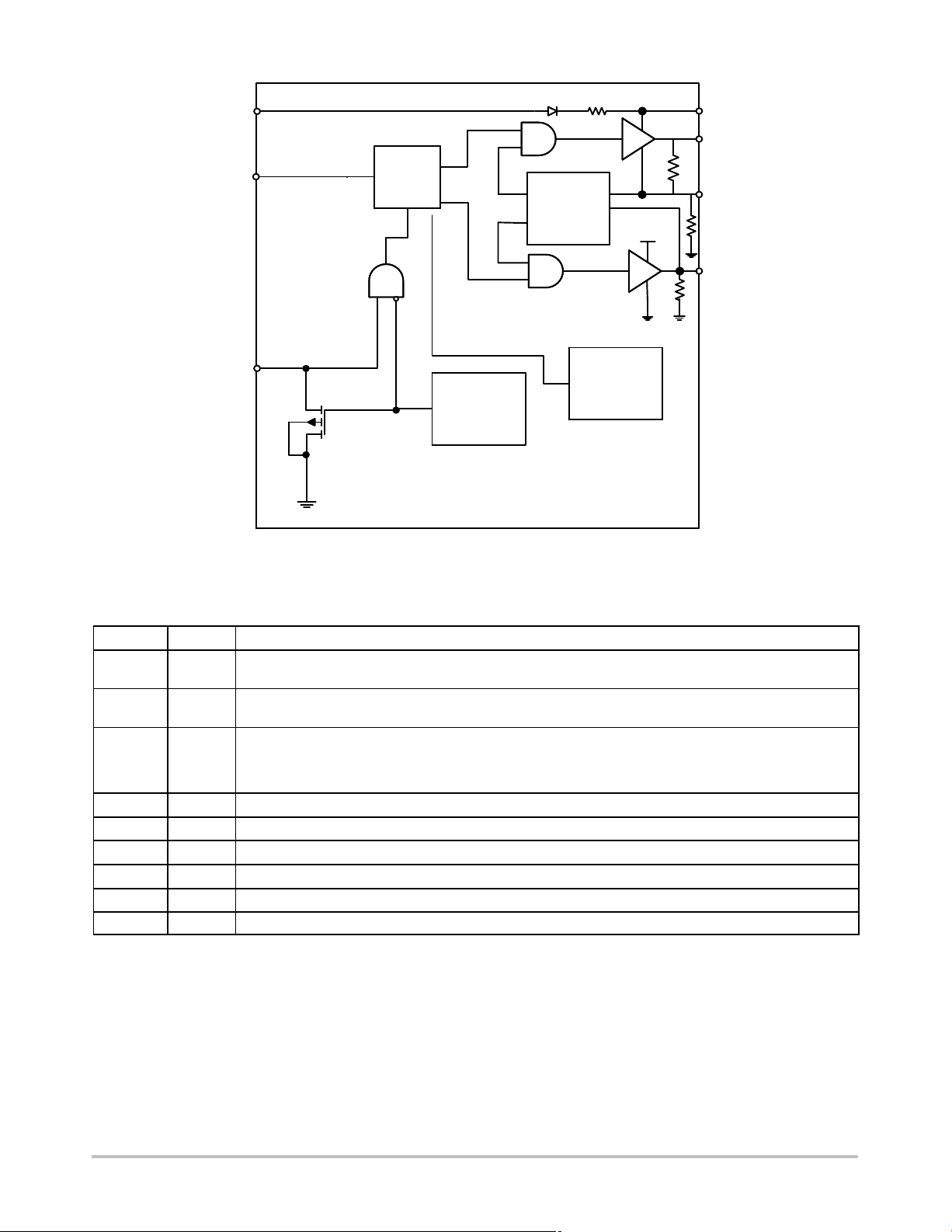
Figure 1. Block Diagram
Anti−Cross
Conduction
BST
DRVH
SW
VCC
DRVL
ZCD
Detection
PIN DESCRIPTIONS
Pin No. Symbol Description
1 BST Floating bootstrap supply pin for high side gate driver. Connect the bootstrap capacitor between this pin and
2 PWM Control input. The PWM signal has three distinctive states: Low = Low Side FET Enabled, Mid = Diode
3 EN Logic input. A logic high to enable the part and a logic low to disable the part. Three states logic input:
4 VCC
5 DRVL Low side gate drive output. Connect to the gate of low side MOSFET.
6 GND Bias and reference ground. All signals are referenced to this node.
7 SW Switch node. Connect this pin to the source of the high side MOSFET and drain of the low side MOSFET.
8 DRVH High side gate drive output. Connect to the gate of high side MOSFET.
9 FLAG Thermal flag. There is no electrical connection to the IC. Connect to ground plane.
the SW pin.
Emulation Enabled, High = High Side FET Enabled.
EN = High to enable the gate driver;
EN = Low to disable the driver;
EN = Mid to go into diode mode (both high and low side gate drive signals are low)
Power supply input. Connect a bypass capacitor (0.1 mF) from this pin to ground.
http://onsemi.com
2

NCP5911
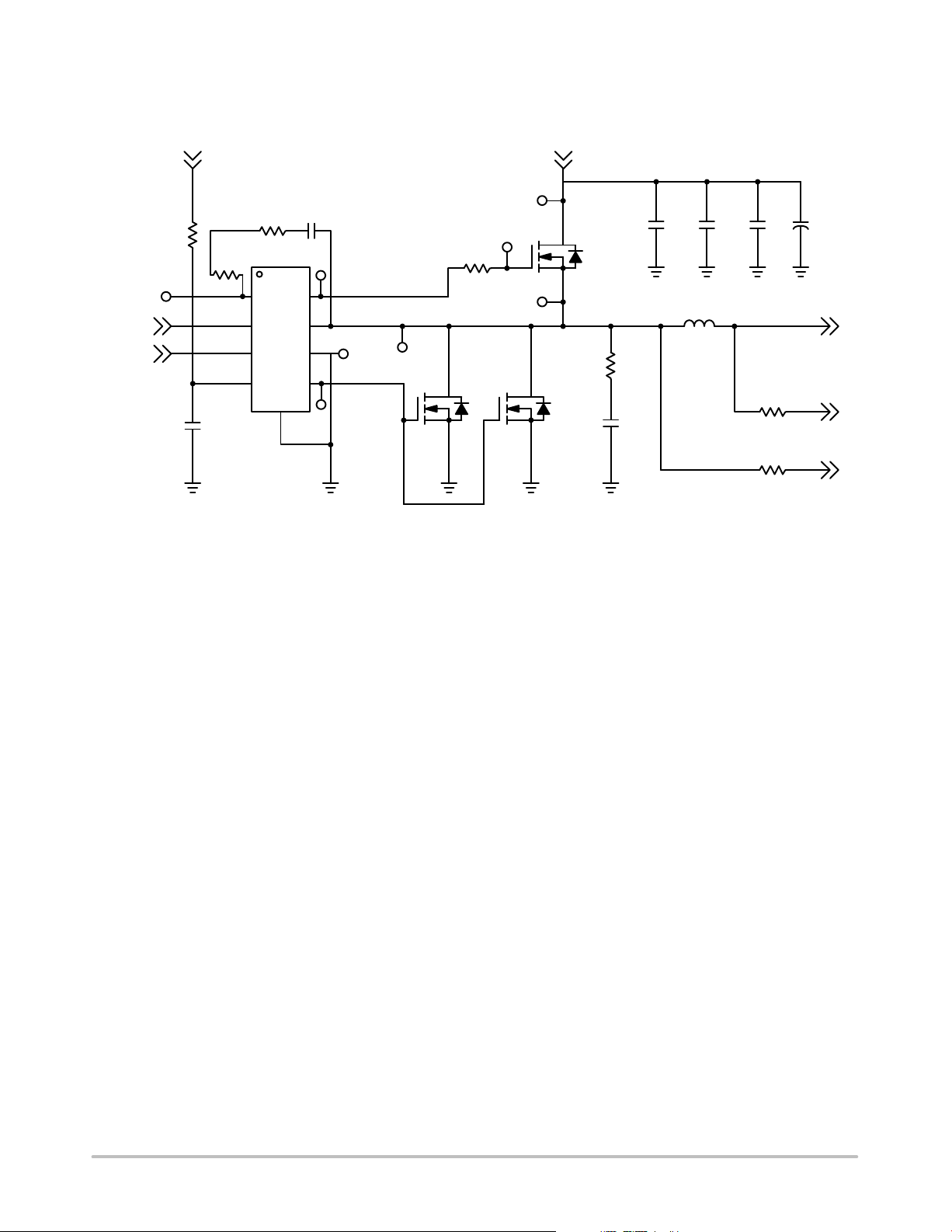
APPLICATION CIRCUIT
TP4
PWM
DRON
5V_POWER
R1
1.02
C5
1uF
R143
0.0
R164
0.0
NCP5911
BST
PWM
EN
VCC
PAD
HG
SW
GND
LG
C4
0.027uF
TP3
VREG_SW1_HG
VREG_SW1_OUT
VREG_SW1_LG
TP8
TP2
R142
0.0
TP6
TP7
Q9 Q10
NTMFS4851N NTMFS4851N
Figure 2. Application Circuit
TP1
TP5
VIN
Q1
NTMFS4821N
C1 C2 C3 CE9
4.7uF 4.7uF 4.7uF 390uF
L
235nH
R3
2.2
C6
2700pF
JP13_ETCH
JP14_ETCH
+
VCCP
CSN11
CSP11
http://onsemi.com
3
 Loading...