

ON NCP500SN185T1, NCP500SN18T1, NCP500SN25T1, NCP500SN26T1, NCP500SN27T1 Schematic [ru]
...
NCP500
150 mA CMOS Low Noise
Low−Dropout Voltage
Regulator
The NCP500 series of fixed output low dropout linear regulators are
designed for portable battery powered applications which require low
noise operation, fast enable response time, and low dropout. The
device achieves its low noise performance without the need of an
external noise bypass capacitor. Each device contains a voltage
reference unit, an error amplifier, a PMOS power transistor, and
resistors for setting output voltage, and current limit and temperature
limit protection circuits.
The NCP500 has been designed to be used with low cost ceramic
capacitors and requires a minimum output capacitor of 1.0 F.
Features
• Ultra−Low Dropout Voltage of 170 mV at 150 mA
• Fast Enable Turn−On Time of 20 sec
• Wide Operating Voltage Range of 1.8 V to 6.0 V
• Excellent Line and Load Regulation
• High Accuracy Output Voltage of 2.5%
• Enable Can Be Driven Directly by 1.0 V Logic
• Typical RMS Noise Voltage 50 V with No Bypass Capacitor
(BW = 10 Hz to 100 kHz)
• Very Small QFN 2x2 Package
• Pb−Free Package May be Available.* The G−Suffix Denotes a
Pb−Free Lead Finish
T ypical Applications
• Noise Sensitive Circuits − VCO’s, RF Stages, etc.
• SMPS Post−Regulation
• Hand−Held Instrumentation
• Camcorders and Cameras
http://onsemi.com
5
1
1
6
PIN CONNECTIONS AND
MARKING DIAGRAMS
TSOP−5
1
V
GND
Enable
Enable
GND
V
in
in
2
3
(Top View)
QFN 2x2
1
2
3
xxxYW
xxM
TSOP−5
SN SUFFIX
CASE 483
QFN 2x2
SQL SUFFIX
CASE 488
5
V
out
4
N/C
6
N/C
5
GND
V
out
4
V
in
1 (3)
Thermal
Shutdown
Enable
3 (1)
ON
OFF
NOTE: Pin numbers in parenthesis indicate QFN package.
Figure 1. Simplified Block Diagram
Semiconductor Components Industries, LLC, 2004
January, 2004 − Rev. 16
Driver w/
Current
Limit
GND
2 (2, 5)
V
out
5 (4)
ORDERING INFORMATION
See detailed ordering and shipping information in the package
dimensions section on page 17 of this data sheet.
*For additional information on our Pb−Free strategy
and soldering details, please download the ON
Semiconductor Soldering and Mounting Techniques
Reference Manual, SOLDERRM/D.
1 Publication Order Number:
(Top View)
xxx, xx = Version
Y = Year
W = Work Week
M = Date Code
NCP500/D
NCP500
Á
Á
Á
Á
PIN FUNCTION DESCRIPTION
TSOP−5
Pin No.
ÁÁ
MAXIMUM RATINGS
Input Voltage
Enable Voltage
Output Voltage
Output Short Circuit Duration
Thermal Resistance, Junction−to−Ambient
TSOP−5
QFN (Note 3)
Operating Junction Temperature
Storage Temperature
1. This device series contains ESD protection and exceeds the following tests:
Human Body Model 2000 V per MIL−STD−883, Method 3015
Machine Model Method 200 V Latch up capability (85°C) 100 mA.
2. Device is internally limited to 160°C by thermal shutdown.
3. For more information, refer to application note, AND8080/D.
QFN 2x2
Pin No.
ÁÁ
1
2
2, 5
3
Pin Name
ÁÁ
3
V
in
GND
1
Enable
ББББББББББББББББББББББ
Positive power supply input voltage.
Power supply ground.
This input is used to place the device into low−power standby. When this input is pulled to a logic
low, the device is disabled. If this function is not used, Enable should be connected to Vin.
4
5
6
4
N/C
V
out
No internal connection.
Regulated output voltage.
Rating Symbol Value Unit
Description
V
in
V
on/off
V
out
−
R
JA
T
J
T
stg
0 to 6.0
−0.3 to V
−0.3 to V
Infinite
250
225
+125
−65 to +150
in
in
+0.3
+0.3
V
V
V
−
°C/W
°C
°C
ELECTRICAL CHARACTERISTICS (V
max values T
= −40°C to 85°C, T
A
Characteristic
jmax
= 2.35 V, Cin = 1.0 F, C
in
= 125°C, unless otherwise noted)
= 1.0 F, for typical value TA = 25°C, for min and
out
Symbol Min Typ Max Unit
−1.8 V
Output Voltage (TA = −40°C to 85°C, I
Line Regulation (Vin = 2.3 V to 6.0 V, I
Load Regulation (I
= 1.0 mA to 150 mA) Reg
out
Dropout Voltage (Measured at V
(Iout = 1.0 mA)
(Iout = 75 mA)
(Iout = 150 mA)
Output Short Circuit Current I
Ripple Rejection
(V
in
= V
+ 1.0 V + 0.5 Vpp, f = 1.0 kHz, Io = 60 mA)
out (nom.)
Quiescent Current
(Enable Input = 0 V)
(Enable Input = 0.9 V, I
(Enable Input = 0.9 V, I
= 1.0 mA)
out
= 150 mA)
out
Enable Input Threshold Voltage
(Voltage Increasing, Output Turns On, Logic High)
(Voltage Decreasing, Output Turns Off, Logic Low)
Enable Input Bias Current I
= 1.0 mA to 150 mA) V
out
= 1.0 mA) Reg
out
−2.0%, T
out
= −40°C to 85°C)
A
1.755 1.8 1.845 V
− 1.0 10 mV
− 15 45 mV
−
−
−
2.0
140
270
10
200
350
200 540 700 mA
V
in−Vout
out(max)
out
line
load
RR − 62 − dB
I
V
th(EN)
IB(EN)
Q
−
−
−
0.9
−
0.01
175
175
−
−
1.0
300
300
−
0.15
− 3.0 100 nA
Output Turn On Time (Enable Input = 0 V to Vin) − − 20 100 s
mV
A
V
http://onsemi.com
2
NCP500
ELECTRICAL CHARACTERISTICS (continued) (V
max values T
= −40°C to 85°C, T
A
Characteristic
= 125°C, unless otherwise noted)
jmax
= 2.35 V, Cin = 1.0 F, C
in
Symbol Min Typ Max Unit
= 1.0 F, for typical value TA = 25°C, for min and
out
−1.85 V
Output Voltage (TA = −40°C to 85°C, I
Line Regulation (Vin = 2.3 V to 6.0 V, I
Load Regulation (I
= 1.0 mA to 150 mA) Reg
out
Dropout Voltage (Measured at V
(Iout = 1.0 mA)
(Iout = 75 mA)
(Iout = 150 mA)
Output Short Circuit Current I
Ripple Rejection
(V
in
= V
+ 1.0 V + 0.5 Vpp, f = 1.0 kHz, Io = 60 mA)
out (nom.)
Quiescent Current
(Enable Input = 0 V)
(Enable Input = 0.9 V, I
(Enable Input = 0.9 V, I
= 1.0 mA)
out
= 150 mA)
out
Enable Input Threshold Voltage
(Voltage Increasing, Output Turns On, Logic High)
(Voltage Decreasing, Output Turns Off, Logic Low)
Enable Input Bias Current I
= 1.0 mA to 150 mA) V
out
= 1.0 mA) Reg
out
−2.0%, T
out
= −40°C to 85°C)
A
1.804 1.85 1.896 V
− 1.0 10 mV
− 15 45 mV
−
−
−
2.0
−
−
−
−
10
200 540 700 mA
V
in−Vout
out(max)
out
line
load
RR − 62 − dB
I
V
th(EN)
IB(EN)
Q
−
−
−
0.9
−
0.01
175
175
−
−
1.0
300
300
−
0.15
− 3.0 100 nA
Output Turn On Time (Enable Input = 0 V to Vin) − − 20 100 s
mV
A
V
ELECTRICAL CHARACTERISTICS (continued) (V
values T
= −40°C to 85°C, T
A
= 125°C, unless otherwise noted)
jmax
Characteristic
= 3.0 V , Cin = 1.0 F, C
in
= 1.0 F, for typical value TA = 25°C, for min and max
out
Symbol Min Typ Max Unit
−2.5 V
Output Voltage
=−40°C to 85°C, I
(T
A
Line Regulation (Vin = 3.0 V to 6.0 V, I
Load Regulation (I
Dropout Voltage (Measured at V
= 1.0 mA to 150 mA)
out
= 1.0 mA) Reg
out
= 1.0 mA to 150 mA) Reg
out
−2.0%, T
out
= −40°C to 85°C)
A
(Iout = 1.0 mA)
(Iout = 75 mA)
(Iout = 150 mA)
Output Short Circuit Current I
Ripple Rejection
(V
in
= V
+ 1.0 V + 0.5 Vpp, f = 1.0 kHz, Io = 60 mA)
out (nom.)
Quiescent Current
(Enable Input = 0 V)
(Enable Input = 0.9 V, I
(Enable Input = 0.9 V, I
= 1.0 mA)
out
= 150 mA)
out
Enable Input Threshold Voltage
(Voltage Increasing, Output Turns On, Logic High)
(Voltage Decreasing, Output Turns Off, Logic Low)
Enable Input Bias Current I
V
out
2.438 2.5 2.563
− 1.0 10 mV
− 15 45 mV
−
−
−
2.0
100
190
10
170
270
200 540 700 mA
V
in−Vout
out(max)
line
load
RR − 62 − dB
I
V
th(EN)
IB(EN)
Q
−
−
−
0.9
−
0.01
180
180
−
−
1.0
300
300
−
0.15
− 3.0 100 nA
Output Turn On Time (Enable Input = 0 V to Vin) − − 20 100 s
V
mV
A
V
http://onsemi.com
3
NCP500
ELECTRICAL CHARACTERISTICS (V
values T
= −40°C to 85°C, T
A
= 125°C, unless otherwise noted)
jmax
Characteristic
= 3.1 V, Cin = 1.0 F, C
in
= 1.0 F, for typical value TA = 25°C, for min and max
out
Symbol Min Typ Max Unit
−2.6 V
Output Voltage
(T
=−40°C to 85°C, I
A
Line Regulation (Vin = 3.0 V to 6.0 V, I
Load Regulation (I
Dropout Voltage (Measured at V
= 1.0 mA to 150 mA)
out
= 1.0 mA) Reg
out
= 1.0 mA to 150 mA) Reg
out
−2.0%, T
out
= −40°C to 85°C)
A
(Iout = 1.0 mA)
(Iout = 75 mA)
(Iout = 150 mA)
Output Short Circuit Current I
Ripple Rejection
(V
in
= V
+ 1.0 V + 0.5 Vpp, f = 1.0 kHz, Io = 60 mA)
out (nom.)
Quiescent Current
(Enable Input = 0 V)
(Enable Input = 0.9 V, I
(Enable Input = 0.9 V, I
= 1.0 mA)
out
= 150 mA)
out
Enable Input Threshold Voltage
(Voltage Increasing, Output Turns On, Logic High)
(Voltage Decreasing, Output Turns Off, Logic Low)
Enable Input Bias Current I
V
out
2.535 2.6 2.665
− 1.0 10 mV
− 15 45 mV
−
−
−
2.0
−
−
−
−
10
200 540 700 mA
V
in−Vout
out(max)
line
load
RR − 62 − dB
I
V
th(EN)
IB(EN)
Q
−
−
−
0.9
−
0.01
180
180
−
−
1.0
300
300
−
0.15
− 3.0 100 nA
Output Turn On Time (Enable Input = 0 V to Vin) − − 20 100 s
V
mV
A
V
ELECTRICAL CHARACTERISTICS (V
values T
= −40°C to 85°C, T
A
= 125°C, unless otherwise noted)
jmax
Characteristic
= 3.2 V, Cin = 1.0 F, C
in
= 1.0 F, for typical value TA = 25°C, for min and max
out
Symbol Min Typ Max Unit
−2.7 V
Output Voltage
=−40°C to 85°C, I
(T
A
Line Regulation (Vin = 3.2 V to 6.0 V, I
Load Regulation (I
Dropout Voltage (Measured at V
= 1.0 mA to 150 mA)
out
= 1.0 mA) Reg
out
= 1.0 mA to 150 mA) Reg
out
−2.0%, T
out
= −40°C to 85°C)
A
(Iout = 1.0 mA)
(Iout = 75 mA)
(Iout = 150 mA)
Output Short Circuit Current I
Ripple Rejection
(V
in
= V
+ 1.0 V + 0.5 Vpp, f = 1.0 kHz, Io = 60 mA)
out (nom.)
Quiescent Current
(Enable Input = 0 V)
(Enable Input = 0.9 V, I
(Enable Input = 0.9 V, I
= 1.0 mA)
out
= 150 mA)
out
Enable Input Threshold Voltage
(Voltage Increasing, Output Turns On, Logic High)
(Voltage Decreasing, Output Turns Off, Logic Low)
Enable Input Bias Current I
V
out
2.633 2.7 2.768
− 1.0 10 mV
− 15 45 mV
−
−
−
2.0
90
180
10
160
260
200 540 700 mA
V
in−Vout
out(max)
line
load
RR − 62 − dB
I
V
th(EN)
IB(EN)
Q
−
−
−
0.9
−
0.01
185
185
−
−
1.0
300
300
−
0.15
− 3.0 100 nA
Output Turn On Time (Enable Input = 0 V to Vin) − − 20 100 s
V
mV
A
V
http://onsemi.com
4

NCP500
ELECTRICAL CHARACTERISTICS (V
values T
= −40°C to 85°C, T
A
= 125°C, unless otherwise noted)
jmax
Characteristic
= 3.3 V, Cin = 1.0 F, C
in
= 1.0 F, for typical value TA = 25°C, for min and max
out
Symbol Min Typ Max Unit
−2.8 V
Output Voltage
(T
=−40°C to 85°C, I
A
Line Regulation (Vin = 3.3 V to 6.0 V, I
Load Regulation (I
Dropout Voltage (Measured at V
= 1.0 mA to 150 mA)
out
= 1.0 mA) Reg
out
= 1.0 mA to 150 mA) Reg
out
−2.0%, T
out
= −40°C to 85°C)
A
(Iout = 1.0 mA)
(Iout = 75 mA)
(Iout = 150 mA)
Output Short Circuit Current I
Ripple Rejection
(V
in
= V
+ 1.0 V + 0.5 Vpp, f = 1.0 kHz, Io = 60 mA)
out (nom.)
Quiescent Current
(Enable Input = 0 V)
(Enable Input = 0.9 V, I
(Enable Input = 0.9 V, I
= 1.0 mA)
out
= 150 mA)
out
Enable Input Threshold Voltage
(Voltage Increasing, Output Turns On, Logic High)
(Voltage Decreasing, Output Turns Off, Logic Low)
Enable Input Bias Current I
V
out
2.730 2.8 2.870
− 1.0 10 mV
− 15 45 mV
−
−
−
2.0
90
170
10
150
250
200 540 700 mA
V
in−Vout
out(max)
line
load
RR − 62 − dB
I
V
th(EN)
IB(EN)
Q
−
−
−
0.9
−
0.01
185
185
−
−
1.0
300
300
−
0.15
− 3.0 100 nA
Output Turn On Time (Enable Input = 0 V to Vin) − − 20 100 s
V
mV
A
V
ELECTRICAL CHARACTERISTICS (V
values T
= −40°C to 85°C, T
A
= 125°C, unless otherwise noted)
jmax
Characteristic
= 3.5 V, Cin = 1.0 F, C
in
= 1.0 F, for typical value TA = 25°C, for min and max
out
Symbol Min Typ Max Unit
−3.0 V
Output Voltage
=−40°C to 85°C, I
(T
A
Line Regulation (Vin = 3.5 V to 6.0 V, I
Load Regulation (I
Dropout Voltage (Measured at V
= 1.0 mA to 150 mA)
out
= 1.0 mA) Reg
out
= 1.0 mA to 150 mA) Reg
out
−2.0%, T
out
= −40°C to 85°C)
A
(Iout = 1.0 mA)
(Iout = 75 mA)
(Iout = 150 mA)
Output Short Circuit Current I
Ripple Rejection
(V
in
= V
+ 1.0 V + 0.5 Vpp, f = 1.0 kHz, Io = 60 mA)
out (nom.)
Quiescent Current
(Enable Input = 0 V)
(Enable Input = 0.9 V, I
(Enable Input = 0.9 V, I
= 1.0 mA)
out
= 150 mA)
out
Enable Input Threshold Voltage
(Voltage Increasing, Output Turns On, Logic High)
(Voltage Decreasing, Output Turns Off, Logic Low)
Enable Input Bias Current I
V
out
2.925 3.0 3.075
− 1.0 10 mV
− 15 45 mV
−
−
−
2.0
85
165
10
130
240
200 540 700 mA
V
in−Vout
out(max)
line
load
RR − 62 − dB
I
V
th(EN)
IB(EN)
Q
−
−
−
0.9
−
0.01
190
190
−
−
1.0
300
300
−
0.15
− 3.0 100 nA
Output Turn On Time (Enable Input = 0 V to Vin) − − 20 100 s
V
mV
A
V
http://onsemi.com
5
NCP500
ELECTRICAL CHARACTERISTICS (V
values T
= −40°C to 85°C, T
A
= 125°C, unless otherwise noted)
jmax
Characteristic
= 3.8 V, Cin = 1.0 F, C
in
= 1.0 F, for typical value TA = 25°C, for min and max
out
Symbol Min Typ Max Unit
−3.3 V
Output Voltage
(T
=−40°C to 85°C, I
A
Line Regulation (Vin = 3.8 V to 6.0 V, I
Load Regulation (I
Dropout Voltage (Measured at V
= 1.0 mA to 150 mA)
out
= 1.0 mA) Reg
out
= 1.0 mA to 150 mA) Reg
out
−2.0%, T
out
= −40°C to 85°C)
A
(Iout = 1.0 mA)
(Iout = 75 mA)
(Iout = 150 mA)
Output Short Circuit Current I
Ripple Rejection
(V
in
= V
+ 1.0 V + 0.5 Vpp, f = 1.0 kHz, Io = 60 mA)
out (nom.)
Quiescent Current
(Enable Input = 0 V)
(Enable Input = 0.9 V, I
(Enable Input = 0.9 V, I
= 1.0 mA)
out
= 150 mA)
out
Enable Input Threshold Voltage
(Voltage Increasing, Output Turns On, Logic High)
(Voltage Decreasing, Output Turns Off, Logic Low)
Enable Input Bias Current I
V
out
3.218 3.3 3.383
− 1.0 10 mV
− 15 45 mV
−
−
−
2.0
80
150
10
110
230
200 540 700 mA
V
in−Vout
out(max)
line
load
RR − 62 − dB
I
V
th(EN)
IB(EN)
Q
−
−
−
0.9
−
0.01
195
195
−
−
1.0
300
300
−
0.15
− 3.0 100 nA
Output Turn On Time (Enable Input = 0 V to Vin) − − 20 100 s
V
mV
A
V
http://onsemi.com
6
NCP500
ELECTRICAL CHARACTERISTICS (V
values T
= −40°C to 85°C, T
A
= 125°C, unless otherwise noted)
jmax
Characteristic
= 5.5 V, Cin = 1.0 F, C
in
= 1.0 F, for typical value TA = 25°C, for min and max
out
Symbol Min Typ Max Unit
−5.0 V
Output Voltage
(T
=−40°C to 85°C, I
A
Line Regulation (Vin = 5.5 V to 6.0 V, I
Load Regulation (I
Dropout Voltage (Measured at V
= 1.0 mA to 150 mA)
out
= 1.0 mA) Reg
out
= 1.0 mA to 150 mA) Reg
out
−2.0%, T
out
= −40°C to 85°C)
A
(Iout = 1.0 mA)
(Iout = 75 mA)
(Iout = 150 mA)
Output Short Circuit Current I
Ripple Rejection
(V
in
= V
+ 1.0 V + 0.5 Vpp, f = 1.0 kHz, Io = 60 mA)
out (nom.)
Quiescent Current
(Enable Input = 0 V)
(Enable Input = 0.9 V, I
(Enable Input = 0.9 V, I
= 1.0 mA)
out
= 150 mA)
out
Enable Input Threshold Voltage
(Voltage Increasing, Output Turns On, Logic High)
(Voltage Decreasing, Output Turns Off, Logic Low)
Enable Input Bias Current I
V
out
4.875 5.0 5.125
− 1.0 10 mV
− 15 45 mV
−
−
−
2.0
60
120
10
100
180
200 540 700 mA
V
in−Vout
out(max)
line
load
RR − 62 − dB
I
V
th(EN)
IB(EN)
Q
−
−
−
0.9
−
0.01
210
210
−
−
1.0
300
300
−
0.15
− 3.0 100 nA
Output Turn On Time (Enable Input = 0 V to Vin) − − 20 100 s
V
mV
A
V
4. Maximum package power dissipation limits must be observed.
T
J(max)TA
PD
R
JA
5. Low duty cycle pulse techniques are used during testing to maintain the junction temperature as close to ambient as possible.
http://onsemi.com
7
NCP500
70
60
50
40
30
Dropout Voltage (mV)
out,
20
− V
in
10
V
0
−50
80
70
60
50
40
Dropout Voltage (mV)
30
out,
20
− V
in
V
10
0
−50
200
V
out(nom.)
= 3.3 V
V
out(nom.)
= 3.3 V
180
50 mA Load
160
150 mA Load
140
120 mA Load
100 mA Load
−25
10 mA Load
50
Temperature (°C)
1.0 mA Load
75250 100
125
Dropout Voltage (mV)
120
out,
− V
100
in
V
80
−50 50 75250 100−25 125
Temperature (°C)
Figure 2. Dropout Voltage vs. Temperature Figure 3. Dropout Voltage vs. Temperature
V
out(nom.)
= 2.8 V
50 mA Load
10 mA Load
1.0 mA Load
−25 75 100 125
0
5025
Temperature (°C)
Figure 4. Dropout Voltage vs. Temperature
220
V
out(nom.)
= 2.8 V
200
180
150 mA Load
160
140
Dropout Voltage (mV)
out,
120
− V
in
100
V
80
−50 50 75250 100−25 125
120 mA Load
100 mA Load
Temperature (°C)
Figure 5. Dropout Voltage vs. Temperature
120
100
80
60
Dropout Voltage (mV)
40
out,
− V
in
20
V
0
−50
V
out(nom.)
= 1.8 V
50 mA Load
10 mA Load
1.0 mA Load
−25 75 100 125
50250
Temperature (°C)
Figure 6. Dropout Voltage vs. Temperature
http://onsemi.com
350
330
V
out(nom.)
= 1.8 V
310
290
150 mA Load
270
250
230
Dropout Voltage (mV)
out,
− V
in
V
210
190
170
120 mA Load
100 mA Load
150
−50 50 75250 100−25 125
Temperature (°C)
Figure 7. Dropout Voltage vs. Temperature
8
NCP500
5
3.308
3.306
3.304
3.302
3.300
3.298
Output Voltage (V)
out,
3.296
V
3.294
3.292
−50
1.804
1.8035
1.803
1.8025
1.802
Output Voltage (V)
1.8015
out,
V
1.801
2.804
Vin = V
V
out(nom.)
= 1.0 mA
I
O
out(nom.)
= 3.3 V
+0.5 V
2.802
2.8
Vin = V
V
out(nom.)
= 1.0 mA
I
O
out(nom.)
= 2.8 V
+ 0.5 V
2.798
2.796
Output Voltage (V)
2.794
out,
V
2.792
2.790
−25
50
Temperature (°C)
75250 100
125 −50 50 75250 100−25 12
Temperature (°C)
Figure 8. Output Voltage vs. Temperature Figure 9. Output Voltage vs. Temperature
210
Vin = V
V
out(nom.)
= 1.0 mA
I
O
out(nom.)
= 1.8 V
+ 0.5 V
Quiescent Current (A)
I
200
190
180
170
Q,
160
Vin = V
I
= 0 mA
O
out(nom.)
= + 0.5 V
V
out(nom.)
V
out(nom.)
= 3.3 V
= 1.8 V
1.8005
−50 50 75250 100−25 125 −50 50 75250 100−25 125
Temperature (°C)
Figure 10. Output Voltage vs. Temperature
225
200
175
150
125
100
75
Quiescent Current (A)
Q,
50
I
25
0
0
1.0
V
out(nom.)
I
= 0 mA
out
= 25°C
T
A
4.0
= 1.8 V
5.03.02.0 6.0
Input Voltage (V)
Figure 12. Quiescent Current vs. Input Voltage
150
Temperature (°C)
Figure 11. Quiescent Current vs. Temperature
225
200
175
150
125
100
75
Quiescent Current (A)
Q,
50
I
25
0
0 4.0 5.03.02.0 6.01.0
V
out(nom.)
I
= 0 mA
out
= 25°C
T
A
Input Voltage (V)
Figure 13. Quiescent Current vs. Input Voltage
= 3.3 V
http://onsemi.com
9

NCP500
225
200
175
150
125
100
75
50
Ground Pin Current (A)
25
0
0 4.0 5.03.02.0 6.01.0 0 4.0 5.03.02.0 6.01.0
V
out(nom.)
I
= 50 mA
out
= 25°C
T
A
= 1.8 V
Input Voltage (V)
Ground Pin Current (A)
225
200
175
150
125
100
75
50
25
V
out(nom.)
I
= 50 mA
out
T
= 25°C
A
0
Input Voltage (V)
Figure 14. Ground Pin Current vs. Input Voltage Figure 15. Ground Pin Current vs. Input Voltage
600
500
400
300
200
Current Limit (mA)
100
0
0 4.0 5.03.02.0 6.01.0 100100.1 1.0
V
out(nom.)
= 3.3 V
Input Voltage (V)
100
80
60 mA
60
40
V
= 1.8 V
20
RR, Ripple Rejection (dB)
out
V
= 2.8 VDC + 0.5 V
in
C
= 1 F
out
0
10 mA
p−p
f, Frequency (kHz)
= 3.3 V
10 mA
1000
800
600
400
200
Output Voltage Noise (nV/HZ)
out,
V
0
0.01 100 1000101.00.1
Figure 16. Current Limit vs. Input Voltage
V
= 1.8 V
out
V
= 2.8 V
in
= 1 mA
I
out
C
= 1 F
out
f, Frequency (kHz)
Figure 18. Output Noise Density
5.0
4.0
3.0
Input Voltage (V)
in,
200
V
150
100
50
0
Output Voltage
Deviation (mV)
−50
Figure 17. Ripple Rejection vs. Frequency
Vin = 3.8 V to 4.8 V
= 3.3 V
V
out
C
= 1.0 F
out
= 1.0 mA
I
out
6040020
10080 120 140 160
Time (s)
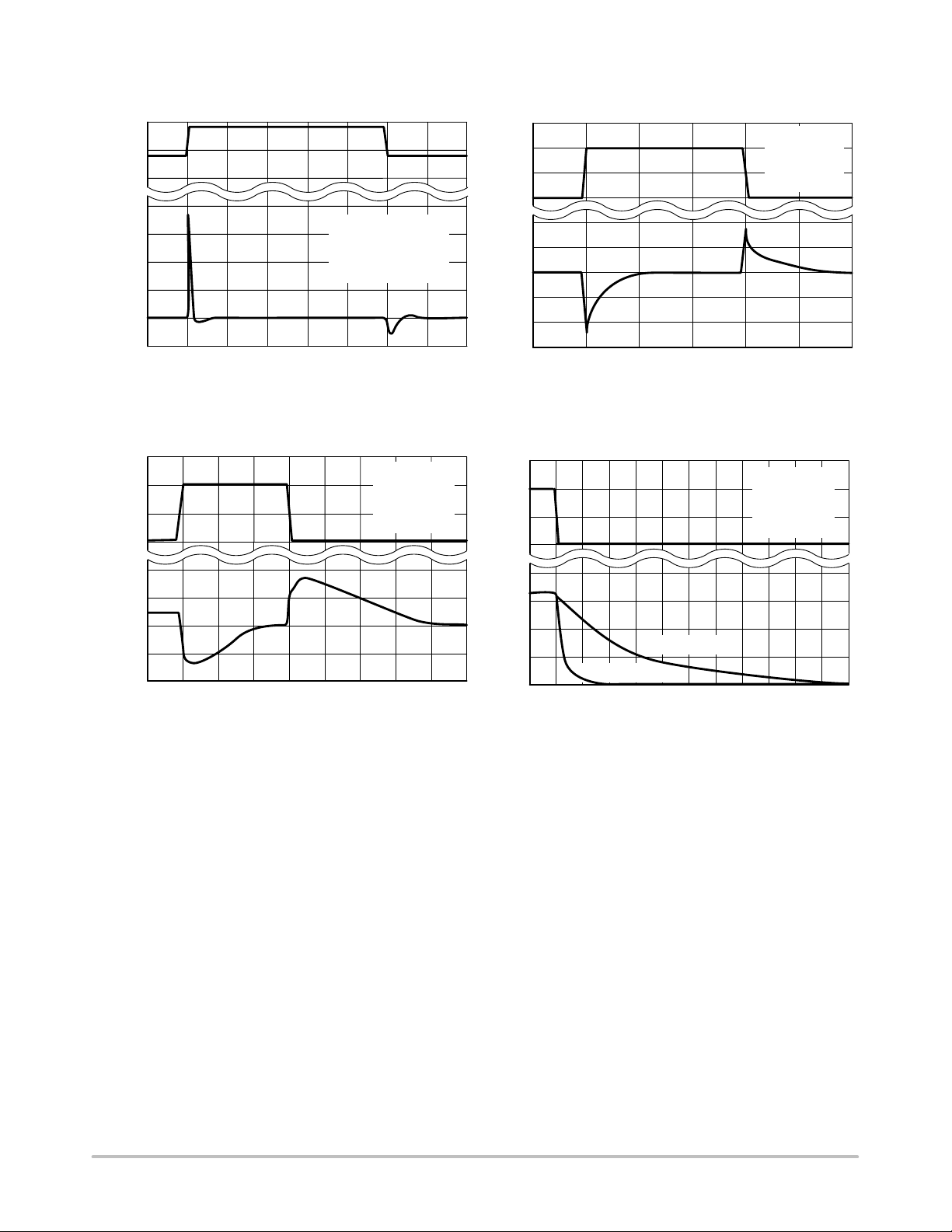
Figure 19. Line Transient Response
http://onsemi.com
10
NCP500
5.0
4.0
Input
in,
V
3.0
Voltage (V)
200
150
100
Vin = 3.8 V to 4.8 V
V
= 3.3 V
out
= 1.0 F
C
out
I
= 10 mA
out
50
Output Voltage
Deviation (mV)
0
−50
0 80 1006040 12020 140 160 0 40 503020 6010
Output
out,
I
Current (mA)
−100
Output Voltage
Deviation (mV)
−200
−300
Time (s) Time (s)
Figure 20. Line Transient Response Figure 21. Load Transient Response
225
150
Output
75
out,
I
Current (mA)
0
50
Vin = 3.8 V
V
= 3.3 V
out
= 10 F
C
out
C
= 1 F
in
225
150
75
200
100
3.0
2.0
1.0
4.0
Vin = 3.8 V
V
= 3.3 V
out
= 1.0 F
C
out
C
= 1 F
in
0
0
Vin = 3.8 V
V
= 3.3 V
out
= 25°C
T
A
= 3.3 k
R
L
Cin = 1 F
0
25
0
−25
Output Voltage
Deviation (mV)
−50
040503020 6010 70 80 90
Time (s)
Figure 22. Load Transient Response
3.0
2.0
1.0
C
= 1.0 F
Output Voltage (V) Enable Voltage (V)
0
out
04020 60
Figure 23. Turn−off Response
C
= 10 F
out
Time (ms)
12080 100
http://onsemi.com
11

NCP500
2
1.8
1.6
1.4
1.2
1
0.8
Output Voltage (V)
0.6
out,
V
0.4
0.2
0
0
3
2.5
2
1.5
Output Voltage (V)
V
out,
0.5
1
0
0453261
V
Input Voltage (V)
in,
C
= 1 F
in
C
= 1 F
out
= 25°C
T
A
V
= V
Enable
1
V
Input Voltage (V)
in,
4
in
5326
C
in
C
out
= 25°C
T
A
V
Enable
= 1 F
= 1 F
= V
in
Figure 24. Output Voltage vs. Input Voltage Figure 25. Output Voltage vs. Input Voltage
3.5
3
2.5
2
1.5
Output Voltage (V)
1
out,
V
0.5
0
0
C
= 1 F
in
C
= 1 F
out
T
= 25°C
A
V
= V
Enable
1567
Input Voltage (V)
V
in,
432
in
Figure 26. Output Voltage vs. Input Voltage
http://onsemi.com
12

NCP500
DEFINITIONS
Load Regulation
The change in output voltage for a change in output load
current at a constant temperature.
Dropout Voltage
The input/output differential at which the regulator output
no longer maintains regulation against further reductions in
input voltage. Measured when the o utput d rops 2% b elow i ts
nominal. The junction temperature, load current, and
minimum input supply r equirements a ffect t he d ropout l e vel.
Output Noise Voltage
This is the integrated value of the output noise over a
specified frequency range. Input voltage and output load
current are kept constant during the measurement. Results
are expressed in
Quiescent Current
VRMS
or nV Hz.
The current which flows through the ground pin when the
regulator operates without a load on its output: internal IC
operation, bias, etc. When the LDO becomes loaded, this
term is called the Ground current. It is actually the difference
between the input current (measured through the LDO input
pin) and the output current.
Line Regulation
The change in output voltage for a change in input voltage.
The measurement is made under conditions of low
dissipation or b y using pulse technique such that the average
chip temperature is not significantly affected.
Line Transient Response
Typical over and undershoot response when input voltage
is excited with a given slope.
Thermal Protection
Internal thermal shutdown circuitry is provided to protect
the integrated circuit in the event that the maximum junction
temperature is exceeded. When activated at typically 160°C,
the regulator turns off. This feature is provided to prevent
failures from accidental overheating.
Maximum Package Power Dissipation
The power dissipation level at which the junction
temperature reaches its maximum operating value, i.e.
125°C.
http://onsemi.com
13

NCP500
APPLICATIONS INFORMATION
The NCP500 series regulators are protected with internal
thermal shutdown and internal current limit. A typical
application circuit is shown in Figure 27.
Input Decoupling (C1)
A 1.0 F capacitor either ceramic or tantalum is
recommended and should be connected close to the NCP500
package. Higher values and lower ESR will improve the
overall line transient response.
Output Decoupling (C2)
The NCP500 is a stable component and does not require
a minimum Equivalent Series Resistance (ESR) or a
minimum output current. The minimum decoupling value is
1.0 F and can be augmented to fulfill stringent load
transient requirements. The regulator accepts ceramic chip
capacitors as well as tantalum devices. Larger values
improve noise rejection and load regulation transient
response. Figure 29 shows the stability region for a range of
operating conditions and ESR values.
Noise Decoupling
The NCP500 is a low noise regulator without the need of
an external bypass capacitor. It t ypically reaches a n oise l evel
of 50 VRMS overall noise b etween 1 0 H z and 1 00 kHz. The
classical bypass capacitor impacts the start up phase of
standard LDOs. However, thanks to its low noise
architecture, the NCP500 operates without a bypass element
and thus offers a typical 20 s start up phase.
Enable Operation
The enable pin will turn on or off the regulator. These
limits of threshold are covered in the electrical specification
section of this data sheet. The turn−on/turn−off transient
voltage being supplied to the enable pin should exceed a
slew rate of 10 mV/s to ensure correct operation. If the
enable is not to be used then the pin should be connected
to V
.
in
Thermal
As power across the NCP500 increases, it might become
necessary to provide some thermal relief. The maximum
power dissipation supported by the device is dependent
upon board design and layout. Mounting pad configuration
on the PCB, the board material, and the ambient temperature
effect the rate of junction temperature rise for the part. This
is stating that when the NCP500 has good thermal
conductivity through the PCB, the junction temperature will
be relatively low with high power dissipation applications.
The maximum dissipation the package can handle is
given by:
T
PD
J(max)TA
R
JA
If TJ is not recommended to exceed 125°C, then the
NCP500 can dissipate up to 400 mW @ 25°C.
The power dissipated by the NCP500 can be calculated
from the following equation:
tot
[
Vin*I
gnd(Iout
P
][
)
Vin V
out
]
*I
out
or
V
inMAX
P
tot
I
gnd
V
I
out
*
out
I
out
If a 150 mA output current is needed the ground current
is extracted from the data sheet curves: 200 A @ 150 mA.
For a NCP500SN18T1 (1.8 V), the maximum input voltage
will then be 4.4 V, good for a 1 Cell Li−ion battery .
Hints
Please be sure the Vin and GND lines are sufficiently wide.
When the impedance of these lines is high, there is a chance
to pick up noise or cause the regulator to malfunction.
Set external components, especially the output capacitor,
as close as possible to the circuit, and make leads as short
as possible.
Package Placement
QFN packages can be placed using standard pick and
place equipment with an accuracy of 0.05 mm.
Component pick and place systems are composed of a vision
system that recognizes and positions the component and a
mechanical system which physically performs the pick and
place operation. Two commonly used types of vision
systems are: (1) a vision system that locates a package
silhouette and (2) a vision system that locates individual
bumps on the interconnect pattern. The latter type renders
more accurate place but tends to be more expensive and time
consuming. Both methods are acceptable since the parts
align due to a self−centering feature of the QFN solder joint
during solder re−flow.
Solder Paste
Type 3 or Type 4 solder paste is acceptable.
Re−flow and Cleaning
The QFN may be assembled using standard IR/IR
convection SMT re−flow processes without any special
considerations. As with other packages, the thermal profile
for specific board locations must be determined. Nitrogen
purge is recommended during solder for no−clean fluxes.
The QFN is qualified for up to three re−flow cycles at 235°C
peak (J−STD−020). The actual temperature of the QFN is a
function of:
• Component density
• Component location on the board
• Size of surrounding components
http://onsemi.com
14

Battery or
Unregulated
Voltage
ON
OFF
C1
NCP500
ON
OFF
V
+
1
5
2
3
4
out
+
C2
Battery or
Unregulated
Voltage
+
C1
1
2
3
6
5
V
4
out
+
C2
Figure 27. Typical Application Circuit
10
UNSTABLE
1
STABLE
0.1
Output Capacitor ESR ()
0.01
0
C
= 1 F to 10 F
out
T
= 40°C to 125°C
A
= up to 6.0 V
V
in
755025
100 125 150
IO, Output Current (mA)
Figure 29. Stability
Figure 28. Typical Application Circuit
Input
R
Q1
Output
1
1.0 F 1.0 F
2
3
5
4
Figure 30. Current Boost Regulator Figure 31. Current Boost Regulator with Short
The NCP500 series can be current boosted with a PNP transistor. Resistor R in conjunction with V
of the PNP determines
BE
when the pass transistor begins conducting; this circuit is not
short circuit proof. Input/Output differential voltage minimum is
increased by V
of the pass resistor.
BE
http://onsemi.com
Input
R1
Q1
R2
Q2
R3
1
1.0 F 1.0 F
2
3
Circuit Limit
Short circuit current limit is essentially set by the V
R1. I
15
SC
= ((V
− ib * R2) / R1) + I
BEQ2
5
4
BE
O(max) Regulator
Output
of Q2 and

NCP500
Input
1
5
1.0 F
2
Enable
3
1
4
5
1.0 F 1.0 F
2
R
3
C
4
Figure 32. Delayed T urn−on Figure 33. Delayed T urn−on
If a delayed turn−on is needed during power up of several voltages then the above schematic can be used. Resistor R, and
capacitor C, will delay the turn−on of the bottom regulator. A
few values were chosen and the resulting delay can be seen in
Figure 33.
Input
R
Q1
1.0 F
Output
1.0 F
Output
4
3
2
1
Enable Voltage (V)
0
TA = 25°C
V
V
3
2.5
2
1.5
1
Output Voltage (V)
0.5
out,
0
V
0
No Delay
20
R = 1.0 M
C = 0.1 F
R = 1.0 M
C = 1.0 F
80
Time (ms)
The graph shows the delay between the enable signal and
output turn−on for various resistor and capacitor values.
Output
1
2
5
1.0 F
= 3.4 V
in
= 2.8 V
out
904030 110
10070605010
3
4
5.6 V
Figure 34. Input Voltages Greater than 6.0 V
A regulated output can be achieved with input voltages that exceed the 6.0 V maximum rating of the NCP500 series with the
addition of a simple pre−regulator circuit. Care must be taken
to prevent Q1 from overheating when the regulated output
(V
) is shorted to G
out
nd.
http://onsemi.com
16

NCP500
ORDERING INFORMATION
Nominal
Device
NCP500SN18T1
NCP500SN185T1
NCP500SN25T1
NCP500SN25T1G
NCP500SN26T1
NCP500SN27T1
NCP500SN28T1
NCP500SN28T1G
NCP500SN30T1
NCP500SN33T1
NCP500SN33T1G
NCP500SN50T1
NCP500SQL18T1
NCP500SQL25T1
NCP500SQL27T1
NCP500SQL28T1
NCP500SQL30T1
NCP500SQL33T1
NCP500SQL50T1
For availability of other output voltages, please contact your local ON Semiconductor Sales Representative.
†For information on tape and reel specifications, including part orientation and tape sizes, please refer to our Tape and Reel Packaging
Specifications Brochure, BRD8011/D.
Output Voltage
1.8
1.85
2.5
2.5
2.6
2.7
2.8
2.8
3.0
3.3
3.3
5.0
1.8
2.5
2.7
2.8
3.0
3.3
5.0
Marking Package Shipping
LCS
LFL
LCT
LCT
LFM
LCU
LCV
LCV
LCW
LCX
LCX
LCY
LD
LE
LF
LG
LH
LJ
LK
TSOP−5 3000 Units/
7″ Tape & Reel
QFN 2x2 3000 Units/
7″ Tape & Reel
†
http://onsemi.com
17

0.05 (0.002)
S
H
D
54
123
L
G
A
NCP500
PACKAGE DIMENSIONS
TSOP−5
SN SUFFIX
PLASTIC PACKAGE
CASE 483−02
ISSUE C
B
C
K
NOTES:
1. DIMENSIONING AND TOLERANCING PER
ANSI Y14.5M, 1982.
2. CONTROLLING DIMENSION: MILLIMETER.
3. MAXIMUM LEAD THICKNESS INCLUDES
LEAD FINISH THICKNESS. MINIMUM LEAD
THICKNESS IS THE MINIMUM THICKNESS
OF BASE MATERIAL.
4. A AND B DIMENSIONS DO NOT INCLUDE
MOLD FLASH, PROTRUSIONS, OR GATE
BURRS.
DIM MIN MAX MIN MAX
A 2.90 3.10 0.1142 0.1220
B 1.30 1.70 0.0512 0.0669
J
M
C 0.90 1.10 0.0354 0.0433
D 0.25 0.50 0.0098 0.0197
G 0.85 1.05 0.0335 0.0413
H 0.013 0.100 0.0005 0.0040
J 0.10 0.26 0.0040 0.0102
K 0.20 0.60 0.0079 0.0236
L 1.25 1.55 0.0493 0.0610
M 0 10 0 10
___ _
S 2.50 3.00 0.0985 0.1181
INCHESMILLIMETERS
SOLDERING FOOTPRINT*
1.9
0.95
0.074
0.037
2.4
0.094
1.0
0.039
0.7
0.028
THIN SOT23−5/TSOP−5/SC59−5
*For additional information on our Pb−Free strategy and soldering
details, please download the ON Semiconductor Soldering and
Mounting Techniques Reference Manual, SOLDERRM/D.
http://onsemi.com
18

NCP500
PACKAGE DIMENSIONS
QFN 2x2.2
SQL SUFFIX
PLASTIC PACKAGE
CASE 488−03
ISSUE C
NOTES:
1. DIMENSIONING AND TOLERANCING PER ANSI
Y14.5M, 1982.
2. CONTROLLING DIMENSION: MILLIMETERS.
3. 488−01 OBSOLETE. NEW STANDARD IS 488−02.
MILLIMETERS
DIMAMIN MAX MIN MAX
TOP VIEW
A
J
H
PIN 1
C
S
2.18 2.23 0.086 0.088
B 1.98 2.03 0.078 0.080
C 0.88 0.93 0.035 0.037
D 0.23 0.28 0.009 0.011
G 0.650 BSC 0.026 BSC
H 0.35 0.40 0.014 0.016
J 0.05 0.10 0.002 0.004
L 1.28 1.33 0.050 0.052
S 0.33 0.38 0.013 0.015
G
B
D
L
INCHES
BOTTOM VIEW
U
SIDE VIEW
http://onsemi.com
19

NCP500
ON Semiconductor and are registered trademarks of Semiconductor Components Industries, LLC (SCILLC). SCILLC reserves the right to make changes without further notice
to any products herein. SCILLC makes no warranty, representation or guarantee regarding the suitability of its products for any particular purpose, nor does SCILLC assume any liability
arising out of the application or use of any product or circuit, and specifically disclaims any and all liability, including without limitation special, consequential or incidental damages.
“Typical” parameters which may be provided in SCILLC data sheets and/or specifications can and do vary in different applications and actual performance may vary over time. All
operating parameters, including “Typicals” must be validated for each customer application by customer’s technical experts. SCILLC does not convey any license under its patent rights
nor the rights of others. SCILLC products are not designed, intended, or authorized for use as components in systems intended for surgical implant into the body, or other applications
intended to support or sustain life, or for any other application in which the failure of the SCILLC product could create a situation where personal injury or death may occur. Should
Buyer purchase or use SCILLC products for any such unintended or unauthorized application, Buyer shall indemnify and hold SCILLC and its officers, employees, subsidiaries, affiliates,
and distributors harmless against all claims, costs, damages, and expenses, and reasonable attorney fees arising out of, directly or indirectly, any claim of personal injury or death
associated with such unintended or unauthorized use, even if such claim alleges that SCILLC was negligent regarding the design or manufacture of the part. SCILLC is an Equal
Opportunity/Affirmative Action Employer. This literature is subject to all applicable copyright laws and is not for resale in any manner.
PUBLICATION ORDERING INFORMATION
LITERATURE FULFILLMENT:
Literature Distribution Center for ON Semiconductor
P.O. Box 5163, Denver, Colorado 80217 USA
Phone: 303−675−2175 or 800−344−3860 Toll Free USA/Canada
Fax: 303−675−2176 or 800−344−3867 Toll Free USA/Canada
Email: orderlit@onsemi.com
N. American Technical Support: 800−282−9855 Toll Free
USA/Canada
Japan: ON Semiconductor, Japan Customer Focus Center
2−9−1 Kamimeguro, Meguro−ku, Tokyo, Japan 153−0051
Phone: 81−3−5773−3850
http://onsemi.com
ON Semiconductor Website: http://onsemi.com
Order Literature: http://www.onsemi.com/litorder
For additional information, please contact your
local Sales Representative.
NCP500/D
20

 Loading...