ON NCP4586DMU12TCG, NCP4586DMU14TCG, NCP4586DMU15TCG, NCP4586DMU18TCG, NCP4586DMU25TCG Schematic [ru]
...
NCP4586
150 mA, Low Noise, Low
Dropout Regulator
The NCP4586 is a CMOS 150 mA low dropout linear with low
noise, high ripple rejection, low dropout, high output voltage accuracy
and low supply current. The device is available in three
configurations: enable high, enable low and enable high plus
auto−discharge. Small packages allow mounting on high density
PCBs. This is an excellent general purpose regulator, well suited to
many applications.
http://onsemi.com
MARKING
DIAGRAMS
Features
• Operating Input Voltage Range: 1.7 V to 6.5 V
• Output Voltage Range: 1.2 to 5.0 V (available in 0.1 V steps)
• Very Low Dropout: 320 mV Typ. at 150 mA
• ±1% Output Voltage Accuracy (V
> 2 V, TJ = 25°C)
OUT
• High PSRR: 80 dB at 1 kHz
• Current Fold Back Protection
• Stable with a 0.47 mF Ceramic Capacitors
• Available in 1.0 x 1.0 UDFN, SC−82AB and SOT23−5 Package
• These are Pb−Free Devices
Typical Applications
• Battery Powered Equipment
• Portable Communication Equipment
• Cameras, MP3 Players and Camcorder
• High Stability Voltage Reference
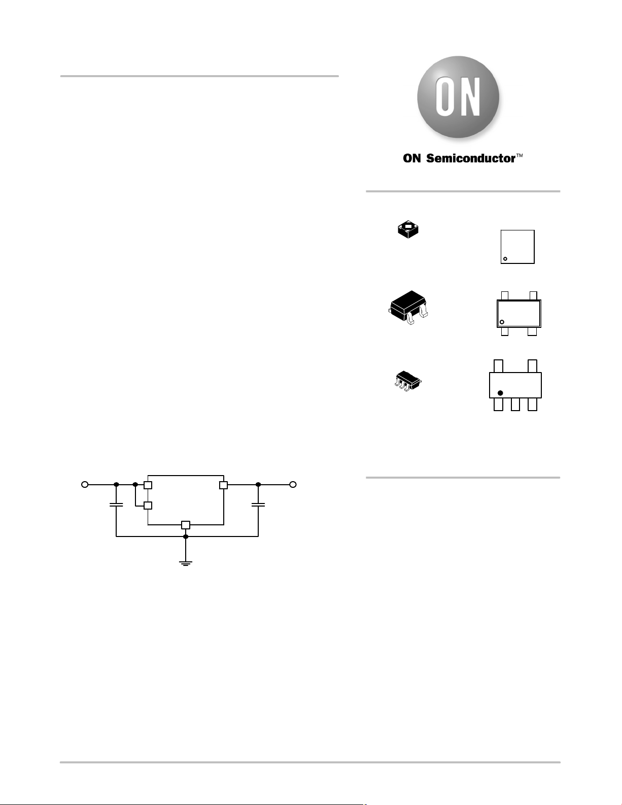
VIN VOUT
C1 C2
470n 470n
NCP4586x
VIN VOUT
CE
GND
1
UDFN4
CASE 517BR
SC−82AB
CASE 419C
SOT−23−5
CASE 1212
XX, XXX= Specific Product Code
MM = Lot Number
ORDERING INFORMATION
See detailed ordering and shipping information in the package
dimensions section on page 15 of this data sheet.
XX
MM
1
XX
MM
1
XXXMM
1
Figure 1. Typical Application Schematic
© Semiconductor Components Industries, LLC, 2012
February, 2012 − Rev. 5
1 Publication Order Number:
NCP4586/D
NCP4586
D
T
VIN
CE
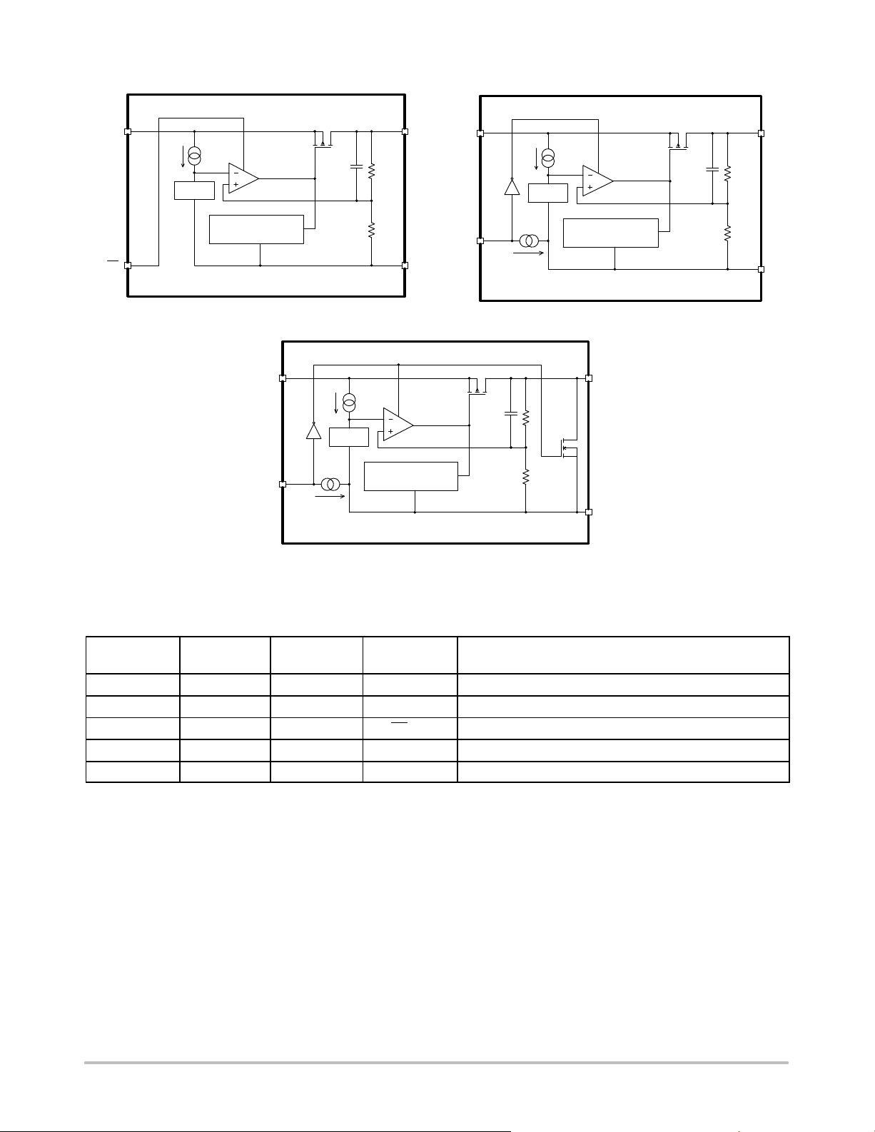
NCP4586Lxxxxxxxx
Vref
Current Limit
VIN
CE
NCP4586Dxxxxxxxx
Vref
Current Limit
VOUT
GND
VIN
CE
NCP4586Hxxxxxxxx
VOU
Vref
Current Limit
GN
VOUT
Figure 2. Simplified Schematic Block Diagram
PIN FUNCTION DESCRIPTION
Pin No.
UDFN4
4 4 1 VIN Input pin
2 2 2 GND Ground
3 1 3 CE/CE Chip enable pin (“L” active / “H” active)
1 3 5 VOUT Output pin
− − 4 NC No connection
Pin No.
SC82−AB
Pin No.
SOT23−5
Pin Name Description
GND
http://onsemi.com
2
NCP4586
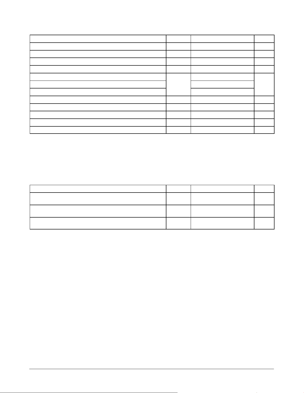
ABSOLUTE MAXIMUM RATINGS
Rating Symbol Value Unit
Input Voltage (Note 1) V
IN
Output Voltage VOUT −0.3 to VIN + 0.3 V
Chip Enable Input VCE −0.3 to 7 V
Output Current I
Power Dissipation UDFN4
OUT
P
D
Power Dissipation SC−82AB 380
Power Dissipation SOT23−5 420
Maximum Junction Temperature T
Operating Ambient Temperature T
Storage Temperature T
ESD Capability, Human Body Model (Note 2) ESD
ESD Capability, Machine Model (Note 2) ESD
J(MAX)
A
STG
HBM
MM
Stresses exceeding Maximum Ratings may damage the device. Maximum Ratings are stress ratings only. Functional operation above the
Recommended Operating Conditions is not implied. Extended exposure to stresses above the Recommended Operating Conditions may affect
device reliability.
1. Refer to ELECTRICAL CHARACTERISTIS and APPLICATION INFORMATION for Safe Operating Area.
2. This device series incorporates ESD protection and is tested by the following methods:
ESD Human Body Model tested per AEC−Q100−002 (EIA/JESD22−A114)
ESD Machine Model tested per AEC−Q100−003 (EIA/JESD22−A115)
Latchup Current Maximum Rating tested per JEDEC standard: JESD78.
7 V
200 mA
400
mW
+150 °C
−40 to +85 °C
−55 to +125 °C
2000 V
200 V
THERMAL CHARACTERISTICS
Rating Symbol Value Unit
Thermal Characteristics, UDFN4
Thermal Resistance, Junction−to−Air
Thermal Characteristics, SOT23−5
Thermal Resistance, Junction−to−Air
Thermal Characteristics, SC 82AB
Thermal Resistance, Junction−to−Air
R
q
JA
R
q
JA
R
q
JA
250 °C/W
238 °C/W
263 °C/W
http://onsemi.com
3
NCP4586
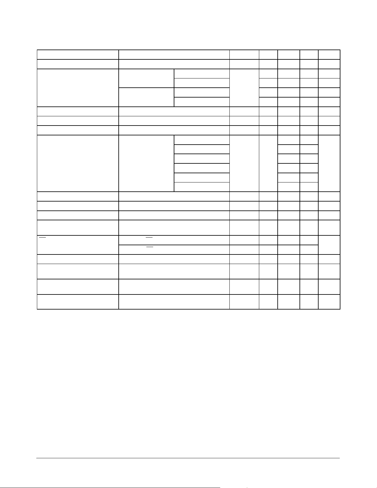
ELECTRICAL CHARACTERISTICS −40°C ≤ T
C
= 0.47 mF, unless otherwise noted. Typical values are at TA = +25 °C.
OUT
Parameter
≤ 85°C; VIN = V
A
OUT(NOM)
+ 1 V or 2.5 V, whichever is greater; I
= 1 mA, CIN =
OUT
Test Conditions Symbol Min Typ Max Unit
Operating Input Voltage VIN 1.7 6.5 V
Output Voltage TA = +25 °C
−40°C ≤ TA ≤ 85°C
V
> 2 V
OUT
V
≤ 2 V −20 20 mV
OUT
V
> 2 V x0.985 x1.015 V
OUT
V
≤ 2 V −30 30 mV
OUT
VOUT
x0.99 x1.01 V
Output Voltage Temp. Coefficient TA = −40 to 85°C ±20 ppm/°C
Line Regulation VIN = VOUT + 0.5 V to 5 V Line
Load Regulation IOUT = 1 mA to 150 mA Load
Dropout Voltage I
= 150 mA
OUT
1.2 V ≤ V
1.5 V ≤ V
1.7 V ≤ V
2.0 V ≤ V
2.5 V ≤ V
4.0 V ≤ V
< 1.5 V
OUT
< 1.7 V 0.54 0.81
OUT
< 2.0 V 0.46 0.68
OUT
< 2.5 V 0.41 0.60
OUT
< 4.0 V 0.32 0.51
OUT
OUT
VDO
Reg
Reg
0.02 0.10 %/V
10 30 mV
0.67 1.00
V
0.24 0.37
Output Current IOUT 150 mA
Short Current Limit V
Quiescent Current IOUT = 0 mA IQ 38 58
Standby Current VCE = V
CE/CE Pin Threshold Voltage
(L version), VCE = 0 V(H and
IN
D version), T
CE / CE Input Voltage “H” VCEH 1.0
= 0 V I
OUT
= 25°C
A
SC
40 mA
ISTB 0.1 1
mA
mA
V
CE / CE Input Voltage “L” VCEL 0.4
CE Pull Down Current H and D version IPD 0.4
Power Supply Rejection Ratio VIN = V
Output Noise Voltage V
Low Output N−ch Tr. On
Resistance
+ 1 V or 3.0 V whichever is higher,
OUT
I
OUT = 30 mA, f = 1 kHz
OUT
= 1.2 V, I
= 30 mA, f = 10 Hz to
OUT
100 kHz
D Version only, VIN = 4 V, VCE = 0 V R
PSRR 80 dB
VN 30
LOW
30
mV
mA
rms
W
http://onsemi.com
4
NCP4586
TYPICAL CHARACTERISTICS
1.4
1.2
1.0
0.8
(V)
OUT
0.6
V
0.4
0.2
0.0
0 100 200 300 400 500
VIN = 2.2 V
6.0 V
6.5 V
I
OUT
(mA)
3.6 V
4.2 V
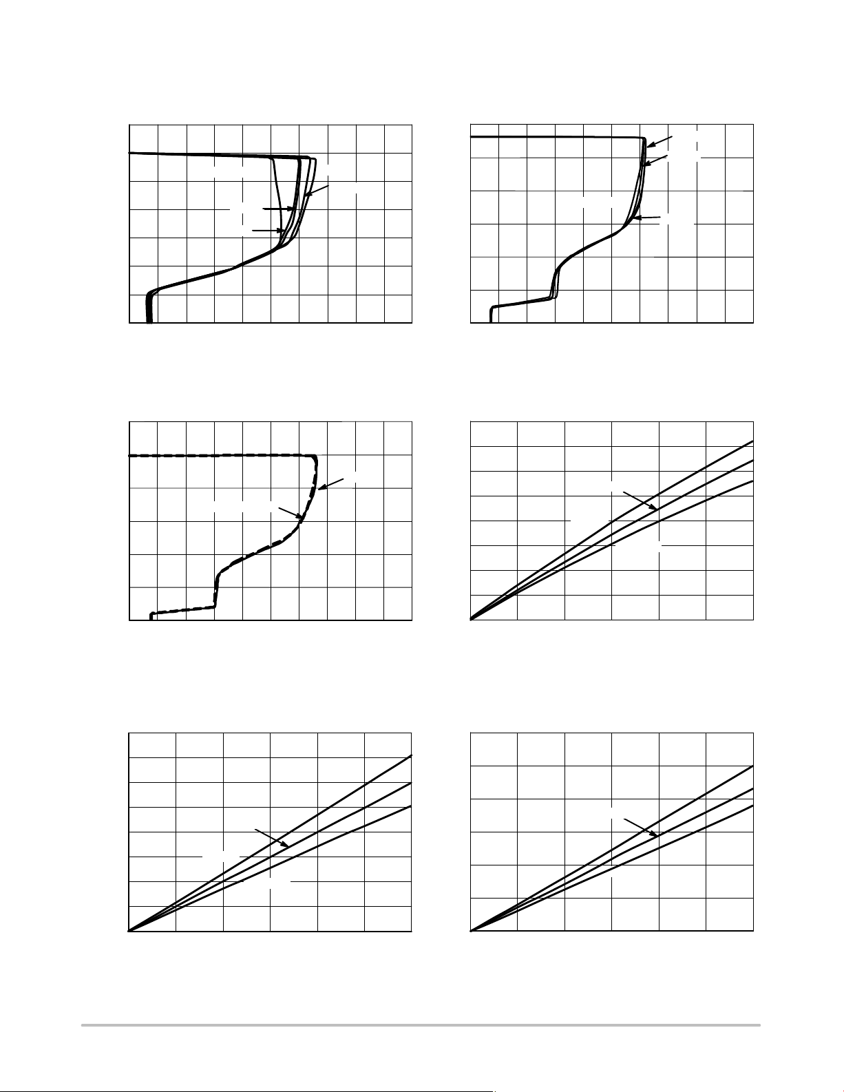
Figure 3. Output Voltage vs. Output Current
(V)
OUT
V
1.2 V Version (T
6
5
4
VIN = 6.5 V
3
2
1
= 25 5C)
A
6.0 V
3.0
2.5
2.0
(V)
1.5
OUT
V
1.0
0.5
0.0
0 100 200 300 400 500
VIN = 6.5 V
I
(mA)
OUT
4.2 V
6.0 V
3.8 V
Figure 4. Output Voltage vs. Output Current
(V)
DO
V
0.8
0.7
0.6
0.5
0.4
0.3
0.2
0.1
2.8 V Version (T
85°C
25°C
= 25 5C)
A
−40°C
0
0 100 200 300 400 500
I
(mA)
OUT
Figure 5. Output Voltage vs. Output Current
5.0 V version (T
0.40
0.35
0.30
0.25
(V)
0.20
DO
V
0.15
0.10
0.05
0.00
0 100 200 300 400 500
85°C
25°C
I
OUT
−40°C
(mA)
= 255C)
A
Figure 7. Dropout Voltage vs. Output Current
2.8 V Version
0
0 100 200 300 400 500
(mA)
I
OUT
Figure 6. Dropout Voltage vs. Output Current
1.2 V version
0.30
0.25
0.20
(V)
0.15
DO
V
0.10
0.05
0.00
0 25 50 75 100 125 150
85°C
I
OUT
25°C
−40°C
(mA)
Figure 8. Dropout Voltage vs. Output Current
5.0 V Version
http://onsemi.com
5
NCP4586
TYPICAL CHARACTERISTICS
1.25
VIN = 2.2 V
1.23
1.21
(V)
OUT
V
1.19
1.17
1.15
−40 −200 20406080
, JUNCTION TEMPERATURE (°C)
T
J
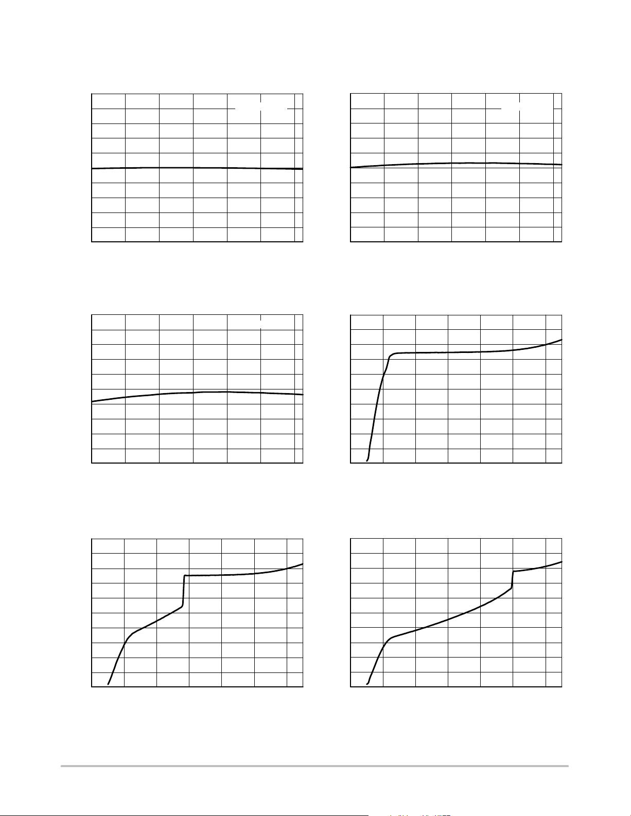
Figure 9. Output Voltage vs. Temperature, 1.2 V
Version
5.05
5.04
5.03
5.02
5.01
(V)
5.00
OUT
V
4.99
4.98
4.97
4.96
4.95
−40 −200 20406080
, JUNCTION TEMPERATURE (°C)
T
J
VIN = 6.0 V
Figure 11. Output Voltage vs. Temperature,
5.0 V Version
2.85
VIN = 3.8 V
2.83
2.81
(V)
OUT
V
2.79
2.77
2.75
−40 −200 20406080
TJ, JUNCTION TEMPERATURE (°C)
Figure 10. Output Voltage vs. Temperature,
2.8 V version
50.0
45.0
40.0
35.0
30.0
25.0
(mA)
IN
I
20.0
15.0
10.0
5.0
0.0
0123456
(V)
V
IN
Figure 12. Supply Current vs. Input Voltage,
1.2 V Version
50.0
45.0
40.0
35.0
30.0
25.0
(mA)
IN
I
20.0
15.0
10.0
5.0
0.0
0123456
VIN (V)
Figure 14. Supply Current vs. Input Voltage,
2.8 V Version
50.0
45.0
40.0
35.0
30.0
25.0
(mA)
IN
I
20.0
15.0
10.0
5.0
0.0
http://onsemi.com
6
0123456
V
(V)
IN
Figure 13. Supply Current vs. Input Voltage,
5.0 V version
 Loading...