

Datasheet NCP4586DMU12TCG, NCP4586DMU14TCG, NCP4586DMU15TCG, NCP4586DMU18TCG, NCP4586DMU25TCG Datasheet (ON) [ru]
...
NCP4586
150 mA, Low Noise, Low
Dropout Regulator
The NCP4586 is a CMOS 150 mA low dropout linear with low
noise, high ripple rejection, low dropout, high output voltage accuracy
and low supply current. The device is available in three
configurations: enable high, enable low and enable high plus
auto−discharge. Small packages allow mounting on high density
PCBs. This is an excellent general purpose regulator, well suited to
many applications.
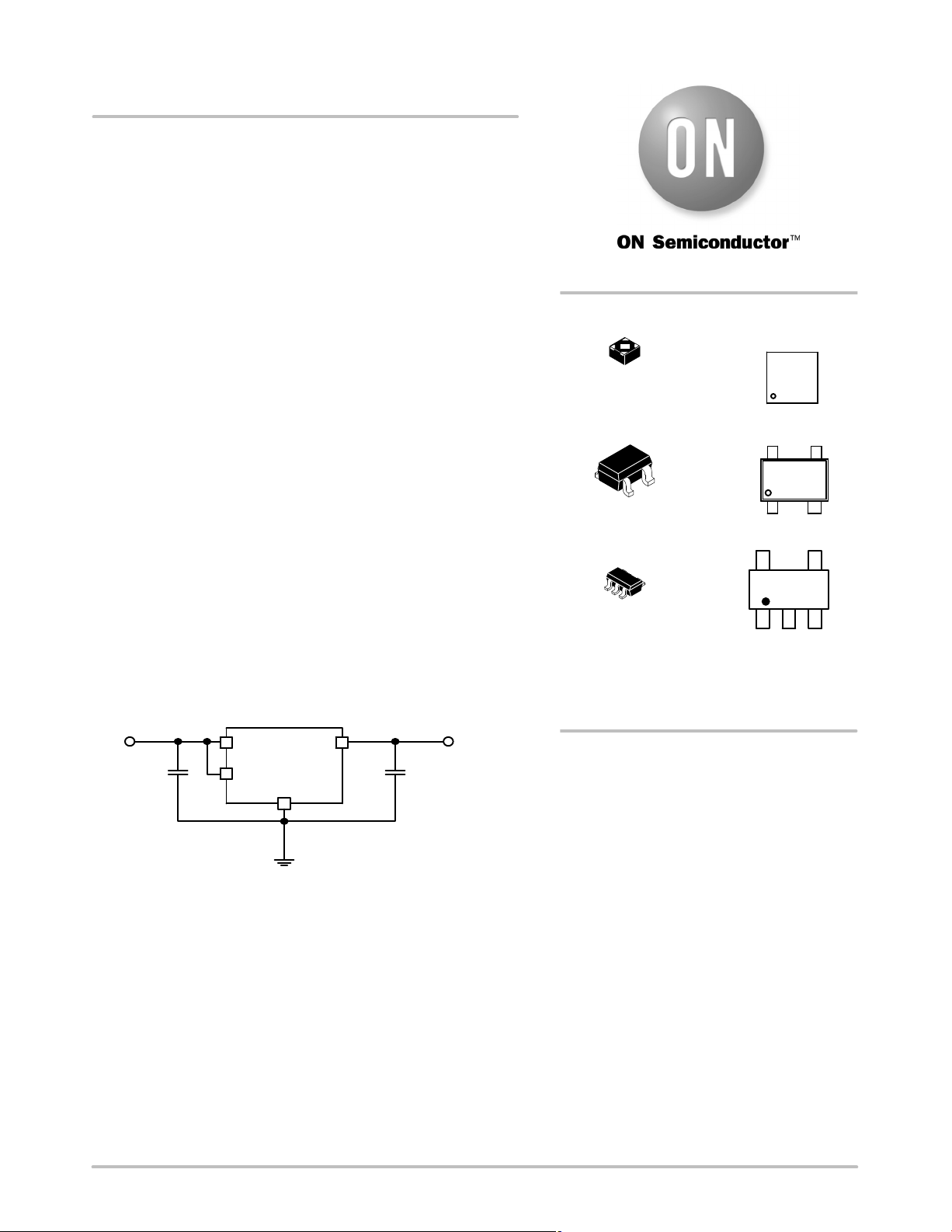
http://onsemi.com
MARKING
DIAGRAMS
Features
• Operating Input Voltage Range: 1.7 V to 6.5 V
• Output Voltage Range: 1.2 to 5.0 V (available in 0.1 V steps)
• Very Low Dropout: 320 mV Typ. at 150 mA
• ±1% Output Voltage Accuracy (V
> 2 V, TJ = 25°C)
OUT
• High PSRR: 80 dB at 1 kHz
• Current Fold Back Protection
• Stable with a 0.47 mF Ceramic Capacitors
• Available in 1.0 x 1.0 UDFN, SC−82AB and SOT23−5 Package
• These are Pb−Free Devices
Typical Applications
• Battery Powered Equipment
• Portable Communication Equipment
• Cameras, MP3 Players and Camcorder
• High Stability Voltage Reference
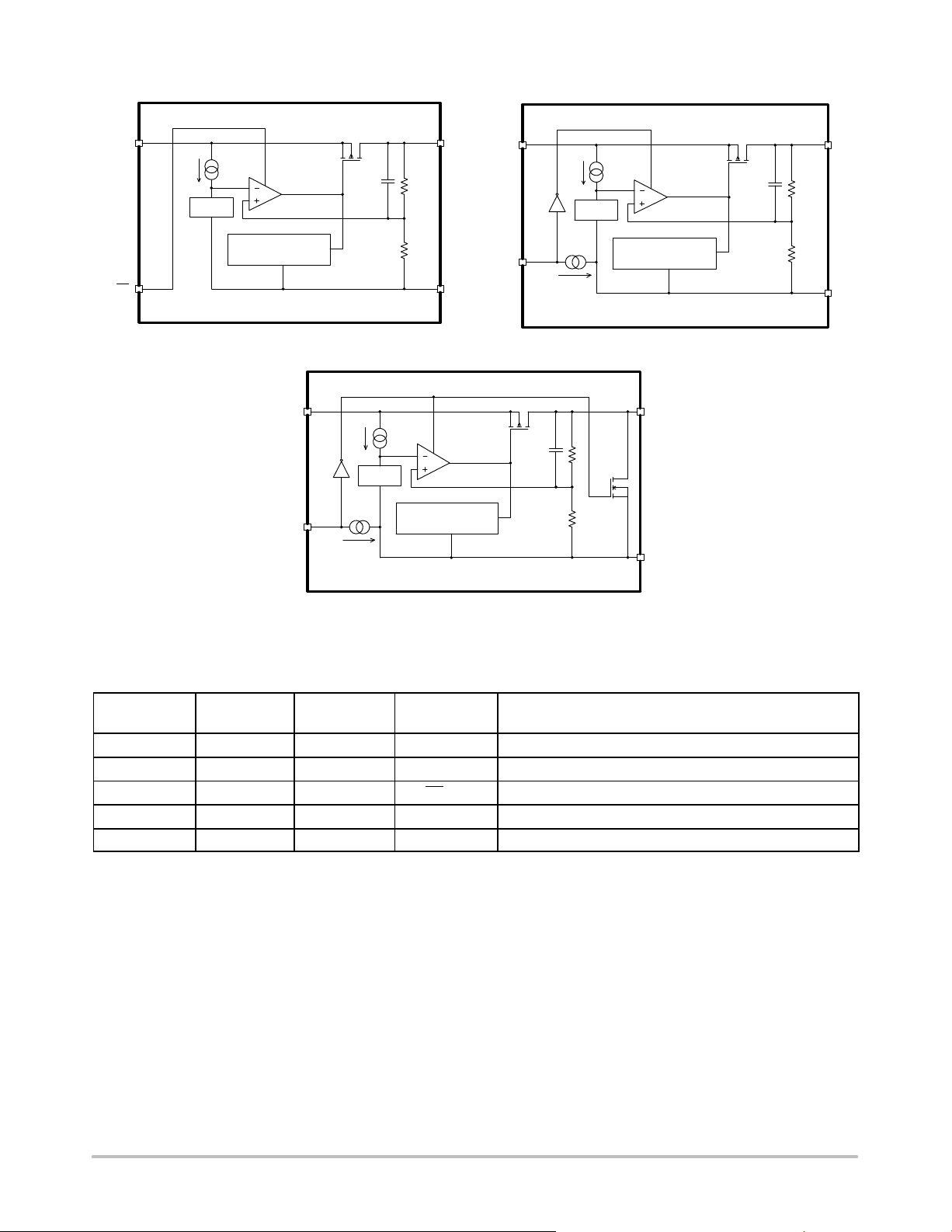
VIN VOUT
C1 C2
470n 470n
NCP4586x
VIN VOUT
CE
GND
1
UDFN4
CASE 517BR
SC−82AB
CASE 419C
SOT−23−5
CASE 1212
XX, XXX= Specific Product Code
MM = Lot Number
ORDERING INFORMATION
See detailed ordering and shipping information in the package
dimensions section on page 15 of this data sheet.
XX
MM
1
XX
MM
1
XXXMM
1
Figure 1. Typical Application Schematic
© Semiconductor Components Industries, LLC, 2012
February, 2012 − Rev. 5
1 Publication Order Number:
NCP4586/D
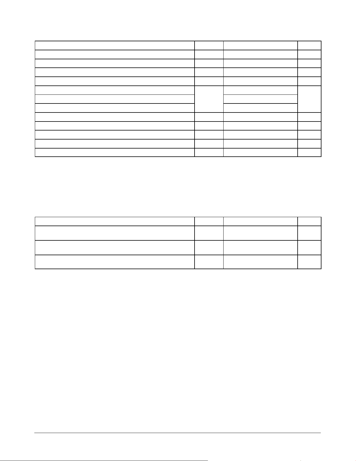
NCP4586
D
T
VIN
CE
NCP4586Lxxxxxxxx
Vref
Current Limit
VIN
CE
NCP4586Dxxxxxxxx
Vref
Current Limit
VOUT
GND
VIN
CE
NCP4586Hxxxxxxxx
VOU
Vref
Current Limit
GN
VOUT
Figure 2. Simplified Schematic Block Diagram
PIN FUNCTION DESCRIPTION
Pin No.
UDFN4
4 4 1 VIN Input pin
2 2 2 GND Ground
3 1 3 CE/CE Chip enable pin (“L” active / “H” active)
1 3 5 VOUT Output pin
− − 4 NC No connection
Pin No.
SC82−AB
Pin No.
SOT23−5
Pin Name Description
GND
http://onsemi.com
2
NCP4586
ABSOLUTE MAXIMUM RATINGS
Rating Symbol Value Unit
Input Voltage (Note 1) V
IN
Output Voltage VOUT −0.3 to VIN + 0.3 V
Chip Enable Input VCE −0.3 to 7 V
Output Current I
Power Dissipation UDFN4
OUT
P
D
Power Dissipation SC−82AB 380
Power Dissipation SOT23−5 420
Maximum Junction Temperature T
Operating Ambient Temperature T
Storage Temperature T
ESD Capability, Human Body Model (Note 2) ESD
ESD Capability, Machine Model (Note 2) ESD
J(MAX)
A
STG
HBM
MM
Stresses exceeding Maximum Ratings may damage the device. Maximum Ratings are stress ratings only. Functional operation above the
Recommended Operating Conditions is not implied. Extended exposure to stresses above the Recommended Operating Conditions may affect
device reliability.
1. Refer to ELECTRICAL CHARACTERISTIS and APPLICATION INFORMATION for Safe Operating Area.
2. This device series incorporates ESD protection and is tested by the following methods:
ESD Human Body Model tested per AEC−Q100−002 (EIA/JESD22−A114)
ESD Machine Model tested per AEC−Q100−003 (EIA/JESD22−A115)
Latchup Current Maximum Rating tested per JEDEC standard: JESD78.
7 V
200 mA
400
mW
+150 °C
−40 to +85 °C
−55 to +125 °C
2000 V
200 V
THERMAL CHARACTERISTICS
Rating Symbol Value Unit
Thermal Characteristics, UDFN4
Thermal Resistance, Junction−to−Air
Thermal Characteristics, SOT23−5
Thermal Resistance, Junction−to−Air
Thermal Characteristics, SC 82AB
Thermal Resistance, Junction−to−Air
R
q
JA
R
q
JA
R
q
JA
250 °C/W
238 °C/W
263 °C/W
http://onsemi.com
3
NCP4586
ELECTRICAL CHARACTERISTICS −40°C ≤ T
C
= 0.47 mF, unless otherwise noted. Typical values are at TA = +25 °C.
OUT
Parameter
≤ 85°C; VIN = V
A
OUT(NOM)
+ 1 V or 2.5 V, whichever is greater; I
= 1 mA, CIN =
OUT
Test Conditions Symbol Min Typ Max Unit
Operating Input Voltage VIN 1.7 6.5 V
Output Voltage TA = +25 °C
−40°C ≤ TA ≤ 85°C
V
> 2 V
OUT
V
≤ 2 V −20 20 mV
OUT
V
> 2 V x0.985 x1.015 V
OUT
V
≤ 2 V −30 30 mV
OUT
VOUT
x0.99 x1.01 V
Output Voltage Temp. Coefficient TA = −40 to 85°C ±20 ppm/°C
Line Regulation VIN = VOUT + 0.5 V to 5 V Line
Load Regulation IOUT = 1 mA to 150 mA Load
Dropout Voltage I
= 150 mA
OUT
1.2 V ≤ V
1.5 V ≤ V
1.7 V ≤ V
2.0 V ≤ V
2.5 V ≤ V
4.0 V ≤ V
< 1.5 V
OUT
< 1.7 V 0.54 0.81
OUT
< 2.0 V 0.46 0.68
OUT
< 2.5 V 0.41 0.60
OUT
< 4.0 V 0.32 0.51
OUT
OUT
VDO
Reg
Reg
0.02 0.10 %/V
10 30 mV
0.67 1.00
V
0.24 0.37
Output Current IOUT 150 mA
Short Current Limit V
Quiescent Current IOUT = 0 mA IQ 38 58
Standby Current VCE = V
CE/CE Pin Threshold Voltage
(L version), VCE = 0 V(H and
IN
D version), T
CE / CE Input Voltage “H” VCEH 1.0
= 0 V I
OUT
= 25°C
A
SC
40 mA
ISTB 0.1 1
mA
mA
V
CE / CE Input Voltage “L” VCEL 0.4
CE Pull Down Current H and D version IPD 0.4
Power Supply Rejection Ratio VIN = V
Output Noise Voltage V
Low Output N−ch Tr. On
Resistance
+ 1 V or 3.0 V whichever is higher,
OUT
I
OUT = 30 mA, f = 1 kHz
OUT
= 1.2 V, I
= 30 mA, f = 10 Hz to
OUT
100 kHz
D Version only, VIN = 4 V, VCE = 0 V R
PSRR 80 dB
VN 30
LOW
30
mV
mA
rms
W
http://onsemi.com
4
NCP4586
TYPICAL CHARACTERISTICS
1.4
1.2
1.0
0.8
(V)
OUT
0.6
V
0.4
0.2
0.0
0 100 200 300 400 500
VIN = 2.2 V
6.0 V
6.5 V
I
OUT
(mA)
3.6 V
4.2 V
Figure 3. Output Voltage vs. Output Current
(V)
OUT
V
1.2 V Version (T
6
5
4
VIN = 6.5 V
3
2
1
= 25 5C)
A
6.0 V
3.0
2.5
2.0
(V)
1.5
OUT
V
1.0
0.5
0.0
0 100 200 300 400 500
VIN = 6.5 V
I
(mA)
OUT
4.2 V
6.0 V
3.8 V
Figure 4. Output Voltage vs. Output Current
(V)
DO
V
0.8
0.7
0.6
0.5
0.4
0.3
0.2
0.1
2.8 V Version (T
85°C
25°C
= 25 5C)
A
−40°C
0
0 100 200 300 400 500
I
(mA)
OUT
Figure 5. Output Voltage vs. Output Current
5.0 V version (T
0.40
0.35
0.30
0.25
(V)
0.20
DO
V
0.15
0.10
0.05
0.00
0 100 200 300 400 500
85°C
25°C
I
OUT
−40°C
(mA)
= 255C)
A
Figure 7. Dropout Voltage vs. Output Current
2.8 V Version
0
0 100 200 300 400 500
(mA)
I
OUT
Figure 6. Dropout Voltage vs. Output Current
1.2 V version
0.30
0.25
0.20
(V)
0.15
DO
V
0.10
0.05
0.00
0 25 50 75 100 125 150
85°C
I
OUT
25°C
−40°C
(mA)
Figure 8. Dropout Voltage vs. Output Current
5.0 V Version
http://onsemi.com
5
NCP4586
TYPICAL CHARACTERISTICS
1.25
VIN = 2.2 V
1.23
1.21
(V)
OUT
V
1.19
1.17
1.15
−40 −200 20406080
, JUNCTION TEMPERATURE (°C)
T
J
Figure 9. Output Voltage vs. Temperature, 1.2 V
Version
5.05
5.04
5.03
5.02
5.01
(V)
5.00
OUT
V
4.99
4.98
4.97
4.96
4.95
−40 −200 20406080
, JUNCTION TEMPERATURE (°C)
T
J
VIN = 6.0 V
Figure 11. Output Voltage vs. Temperature,
5.0 V Version
2.85
VIN = 3.8 V
2.83
2.81
(V)
OUT
V
2.79
2.77
2.75
−40 −200 20406080
TJ, JUNCTION TEMPERATURE (°C)
Figure 10. Output Voltage vs. Temperature,
2.8 V version
50.0
45.0
40.0
35.0
30.0
25.0
(mA)
IN
I
20.0
15.0
10.0
5.0
0.0
0123456
(V)
V
IN
Figure 12. Supply Current vs. Input Voltage,
1.2 V Version
50.0
45.0
40.0
35.0
30.0
25.0
(mA)
IN
I
20.0
15.0
10.0
5.0
0.0
0123456
VIN (V)
Figure 14. Supply Current vs. Input Voltage,
2.8 V Version
50.0
45.0
40.0
35.0
30.0
25.0
(mA)
IN
I
20.0
15.0
10.0
5.0
0.0
http://onsemi.com
6
0123456
V
(V)
IN
Figure 13. Supply Current vs. Input Voltage,
5.0 V version

NCP4586
TYPICAL CHARACTERISTICS
40.0
39.0
38.0
37.0
36.0
35.0
(mA)
IN
I
34.0
33.0
32.0
31.0
30.0
−40 −20 0 20 40 60 80
TJ, JUNCTION TEMPERATURE (°C)
Figure 15. Supply Current vs. Temperature,
1.2 V Version
45
44
43
42
41
40
(mA)
IN
I
39
38
37
36
35
−40 −20 0 20 40 60 80
TJ, JUNCTION TEMPERATURE (°C)
Figure 17. Supply Current vs. Temperature,
5.0 V Version
VIN = 2.2 V
VIN = 6.0 V
40.0
39.0
38.0
37.0
36.0
35.0
(mA)
IN
I
34.0
33.0
32.0
31.0
30.0
VIN = 3.8 V
−40 −200 20406080
, JUNCTION TEMPERATURE (°C)
T
J
Figure 16. Supply Current vs. Temperature,
2.8 V Version
1.4
1.2
1.0
1 mA
0.8
(V)
OUT
0.6
V
0.4
0.2
0.0
01234567
I
OUT
30 mA
= 50 mA
VIN (V)
Figure 18. Output Voltage vs. Input Voltage,
1.2 V Version
3.0
2.5
2.0
(V)
1.5
OUT
V
1.0
0.5
0.0
01234567
1 mA
I
OUT
30 mA
= 50 mA
VIN (V)
Figure 19. Output Voltage vs. Input Voltage,
2.8 V Version
http://onsemi.com
6.0
5.0
4.0
(V)
3.0
OUT
V
2.0
1 mA
1.0
0.0
01234567
I
OUT
30 mA
= 50 mA
VIN (V)
Figure 20. Output Voltage vs. Input Voltage,
5.0 V Version
7

NCP4586
TYPICAL CHARACTERISTICS
100
90
80
1 mA
30 mA
70
I
= 150 mA
OUT
60
50
40
PSRR (dB)
30
20
10
0
0.01 0.1 1 10 100 1000
FREQUENCY (kHz)
Figure 21. PSRR, 1.2 V Version
100
90
80
70
60
30 mA
I
OUT
1 mA
= 150 mA
50
40
PSRR (dB)
30
20
10
0
0.01 0.1 1 10 100 1000
FREQUENCY (kHz)
Figure 23. PSRR, 5.0 V Version
100
90
80
70
I
OUT
1 mA
30 mA
= 150 mA
60
50
40
PSRR (dB)
30
20
10
0
0.01 0.1 1 10 100 1000
FREQUENCY (kHz)
Figure 22. PSRR, 2.8 V Version
1.6
1.4
1.2
1.0
/√Hz)
0.8
rms
(mV
0.6
N
V
0.4
0.2
0
0.01 0.1 1 10 100 1000
FREQUENCY (kHz)
Figure 24. Output Voltage Noise, 1.2 V Version
7.0
6.0
5.0
/√Hz)
4.0
rms
3.0
(mV
N
V
2.0
1.0
0
0.01 0.1 1 10 100 1000
FREQUENCY (kHz)
Figure 25. Output Voltage Noise, 2.8 V Version
http://onsemi.com
7.0
6.0
5.0
/√Hz)
4.0
rms
3.0
(mV
N
V
2.0
1.0
0
0.01 0.1 1 10 100 1000
FREQUENCY (kHz)
Figure 26. Output Voltage Noise, 5.0 V Version
8

NCP4586
TYPICAL CHARACTERISTICS
4
3
2
(V)
1.205
OUT
V
1.200
1.195
1.190
0 102030405060708090100
t (ms)
Figure 27. Line Transients, 1.2 V Version,
t
(V)
OUT
2.805
V
2.800
2.795
= tF = 5 ms, I
R
OUT
= 30 mA
1
(V)
IN
V
6
5
4
3
(V)
IN
V
2.790
0 10203040 5060708090100
t (ms)
Figure 28. Line Transients, 2.8 V Version,
t
= tF = 5 ms, I
R
(V)
5.005
OUT
V
5.000
4.995
4.990
0 102030405060708090100
t (ms)
OUT
= 30 mA
Figure 29. Line Transients, 5.0 V Version, tR =
t
= 5 ms, I
F
OUT
= 30 mA
7
6
5
4
(V)
IN
V
http://onsemi.com
9

NCP4586
TYPICAL CHARACTERISTICS
(V)
OUT
V
1.23
1.22
1.21
1.20
1.19
1.18
0 10 2030405060708090100
t (ms)
Figure 30. Load Transients, 1.2 V Version,
I
= 50 − 100 mA, tR = tF = 0.5 ms, V
OUT
(V)
OUT
V
2.83
2.82
2.81
2.80
2.79
2.78
0 10203040 5060708090100
t (ms)
Figure 31. Load Transients, 2.8 V Version,
I
= 50 − 100 mA, tR = tF = 0.5 ms, V
OUT
IN
IN
= 2.2 V
= 3.8 V
200
150
100
50
0
200
150
100
50
0
(mA)
OUT
I
(mA)
OUT
I
(V)
OUT
V
5.03
5.02
5.01
4.99
4.98
0 10203040 5060708090100
t (ms)
Figure 32. Load Transients, 5.0 V Version,
I
= 50 − 100 mA, tR = tF = 0.5 ms, V
OUT
IN
http://onsemi.com
10
= 6.0 V
200
150
100
50
0
(mA)
OUT
I

NCP4586
TYPICAL CHARACTERISTICS
(V)
OUT
V
1.30
1.25
1.20
1.15
1.10
1.05
0 10203040 5060708090100
t (ms)
Figure 33. Load Transients, 1.2 V Version,
I
= 1 − 150 mA, tR = tF = 0.5 ms, V
OUT
= 2.2 V
IN
200
150
100
50
0
200
150
(mA)
OUT
I
(V)
OUT
V
2.90
2.85
2.80
2.75
2.70
2.65
0 10203040 5060708090100
t (ms)
Figure 34. Load Transients, 2.8 V Version,
I
= 1 − 150 mA, tR = tF = 0.5 ms, V
OUT
(V)
OUT
V
5.10
5.05
5.00
4.95
4.90
4.85
0 10 2030405060708090100
t (ms)
= 3.8 V
IN
Figure 35. Load Transients, 5.0 V Version,
I
= 1 − 150 mA, tR = tF = 0.5 ms, V
OUT
= 6.0 V
IN
100
50
0
200
150
100
50
0
(mA)
OUT
I
(mA)
OUT
I
http://onsemi.com
11

NCP4586
TYPICAL CHARACTERISTICS
Chip Enable
(V)
2.0
OUT
V
1.5
1.0
0.5
0.0
−0.5
0 2 4 6 8 101214161820
Figure 36. Start−up, 1.2 V Version, VIN = 2.2 V
t (ms)
I
OUT
I
OUT
= 150 mA
= 1 mA
4
3
2
1
0
(V)
CE
V
Chip Enable
(V)
4
OUT
V
3
2
1
I
OUT
= 1 mA
I
OUT
= 150 mA
0
−1
02468101214161820
t (ms)
Figure 37. Start−up, 2.8 V Version, V
= 3.8 V
IN
Chip Enable
(V)
8
OUT
V
6
4
I
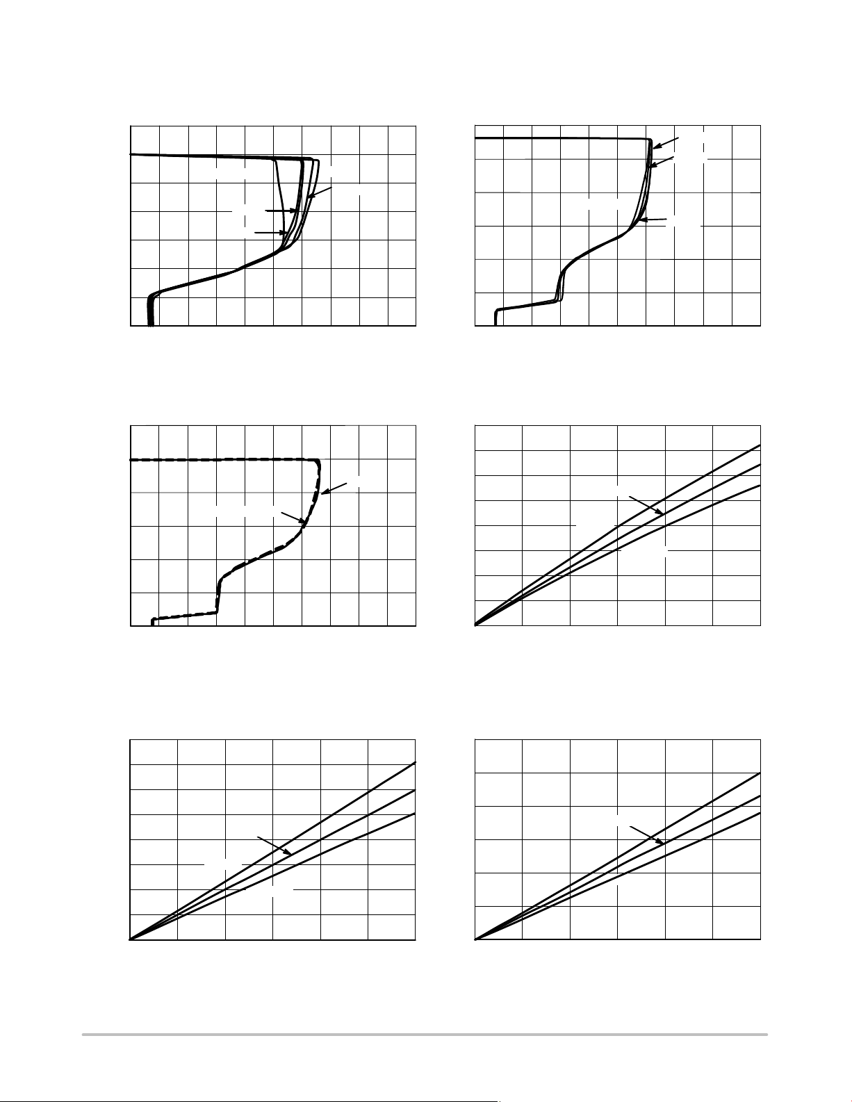
= 1 mA
OUT
2
I
OUT
= 150 mA
0
−2
0 5 10 15 20 25 30 35 40 45 50
t (ms)
Figure 38. Start−up, 5.0 V Version, V
= 6.0 V
IN
5
4
3
2
1
10
8
6
4
2
0
(V)
CE
V
(V)
CE
V
http://onsemi.com
12

NCP4586
TYPICAL CHARACTERISTICS
Chip Enable
(V)
2.0
OUT
V
1.5
I
= 1 mA
= 150 mA
OUT
V
I
t (ms)
= 2.2 V
IN
OUT
= 30 mA
1.0
0.5
0.0
I
−0.5
OUT
0 102030 405060708090100
Figure 39. Shutdown, 1.2 V Version D,
4
3
2
1
0
(V)
CE
V
5
4
= 1 mA
Chip Enable
I
= 30 mA
OUT
(V)
OUT
V
2.0
1.5
1.0
0.5
0.0
−0.5
I
OUT
I
OUT
= 150 mA
0 102030405060708090100
t (ms)
Figure 40. Shutdown, 2.8 V Version D,
V
= 3.8 V
IN
(V)
8
OUT
V
6
4
I
OUT
= 1 mA
2
0
I
= 150 mA
OUT
−2
0 102030405060708090100
Chip Enable
I
= 30 mA
OUT
t (ms)
Figure 41. Shutdown, 5.0 V version D,
V
= 6.0 V
IN
3
2
1
10
8
6
4
2
0
(V)
CE
V
(V)
CE
V
http://onsemi.com
13

NCP4586
APPLICATION INFORMATION
A typical application circuit for NCP4586 series is shown
in Figure 42.
VIN VOUT
C1 C2
470n 470n
Figure 42. Typical Application Schematic
Input Decoupling Capacitor (C1)
NCP4586 x
VIN VOUT
CE
GND
A 470 nF ceramic input decoupling capacitor should be
connected as close as possible to the input and ground pin of
the NCP4586. Higher values and lower ESR improves line
transient response.
Output Decoupling Capacitor (C2)
A 470 nF or larger ceramic output decoupling capacitor is
sufficient to achieve stable operation of the IC. If a tantalum
capacitor is used, and its ESR is high, loop oscillation may
result. The capacitors should be connected as close as
possible to the output and ground pins. Larger values and
lower ESR improves dynamic parameters.
version of IC. Active high or low versions are available;
please see the ordering information table. The Enable pin
has an internal pull down current source for versions H and
D. If the enable function is not needed connect the CE
pin to
ground for version L or connect the CE pin to VIN for
versions H and D.
Output Discharger
The D version includes a transistor between VOUT and
GND that is used for faster discharging of the output
capacitor. This function is activated when the IC goes into
disable mode.
Thermal
As power across the IC increases, it might become
necessary to provide some thermal relief. The maximum
power dissipation supported by the device is dependent
upon board design and layout. Mounting pad configuration
on the PCB, the board material, and also the ambient
temperature affect the rate of temperature rise for the part.
That is to say, when the device has good thermal
conductivity through the PCB, the junction temperature will
be relatively low with high power dissipation applications.
PCB Layout
Make VIN and GND line sufficient. If their impedance is
high, noise pickup or unstable operation may result. Connect
capacitors C1 and C2 as close as possible to the IC, and make
wiring as short as possible.
Enable Operation
The Enable pin CE or CE may be used for turning the
regulator on and off. Control polarity is dependent on
http://onsemi.com
14

NCP4586
ORDERING INFORMATION
Nominal Output
Device
NCP4586DSQ12T1G 1.2 V
NCP4586DSQ18T1G 1.8 V LG
NCP4586DSQ28T1G 2.8 V MH
NCP4586DSQ30T1G 3.0 V NA
NCP4586DSQ33T1G 3.3 V ND
NCP4586DSQ50T1G 5.0 V QA
NCP4586DMU12TCG 1.2 V VA
NCP4586DMU14TCG 1.4 V VC
NCP4586DMU15TCG 1.5 V VD
NCP4586DMU18TCG 1.8 V VG
NCP4586DMU25TCG 2.5 V VQ
NCP4586DMU28TCG 2.8 V VT
NCP4586DMU30TCG 3.0 V VW
NCP4586DMU33TCG 3.3 V VZ
NCP4586DMU50TCG 5.0 V WS
NCP4586DSN12T1G 1.2 V H2A
NCP4586DSN18T1G 1.8 V H2G
NCP4586DSN28T1G 2.8 V H2T
NCP4586DSN30T1G 3.0 V H2W
NCP4586DSN33T1G 3.3 V H2Z
NCP4586DSN50T1G 5.0 V J2S
†For information on tape and reel specifications, including part orientation and tape sizes, please refer to our Tape and Reel Packaging
Specifications Brochure, BRD8011/D.
NOTE: To order other package and voltage variants, please contact your ON Semiconductor sales representative.
Voltage
Description Marking Package Shipping
LA
Enable High,
Auto discharge
SC82AB
(Pb−Free)
UDFN4
(Pb−Free)
SOT−23−5
(Pb−Free)
3000 / Tape & Reel
10000 / Tape & Reel
3000 / Tape & Reel
†
http://onsemi.com
15

PIN ONE
REFERENCE
2X
0.05 C
2X
0.05 C
0.05 C
NOTE 4
DETAIL A
D2
45 5
0.05 C
TOP VIEW
SIDE VIEW
e
1
4
BOTTOM VIEW
NCP4586
PACKAGE DIMENSIONS
UDFN4 1.0x1.0, 0.65P
CASE 517BR−01
ISSUE O
4X
D
A
L3
B
c 0.18
E
L2
DETAIL A
typ
3X
0.43
4X
0.23
(A3)
A
3X
0.10
A1
C
SEATING
PLANE
DETAIL B
MOUNTING FOOTPRINT*
e/2
3X
4X
L
D2
b
M
0.05 BC
A
NOTE 3
PITCH
DETAIL B
PACKAGE
OUTLINE
0.53
*For additional information on our Pb−Free strategy and soldering
details, please download the ON Semiconductor Soldering and
Mounting Techniques Reference Manual, SOLDERRM/D.
2
3
NOTES:
1. DIMENSIONING AND TOLERANCING PER
ASME Y14.5M, 1994.
2. CONTROLLING DIMENSION: MILLIMETERS.
3. DIMENSION b APPLIES TO PLATED TERMINAL
AND IS MEASURED BETWEEN 0.15 AND
0.20 mm FROM TERMINAL.
4. COPLANARITY APPLIES TO THE EXPOSED
PAD AS WELL AS THE TERMINALS.
DIM MIN MAX
A −−− 0.60
A1 0.00 0.05
A3 0.10 REF
b 0.20 0.30
D 1.00 BSC
D2 0.43 0.53
E 1.00 BSC
e 0.65 BSC
L 0.20 0.30
L2 0.27 0.37
L3 0.02 0.12
RECOMMENDED
0.65
DIMENSIONS: MILLIMETERS
MILLIMETERS
2X
1.30
4X
0.30
0.52
http://onsemi.com
16

D 3 PL
S
A
G
4
3
12
NCP4586
PACKAGE DIMENSIONS
SC−82AB
CASE 419C−02
ISSUE E
C
N
B
F
L
K
H
J
0.05 (0.002)
SOLDERING FOOTPRINT*
NOTES:
1. DIMENSIONING AND TOLERANCING PER
ANSI Y14.5M, 1982.
2. CONTROLLING DIMENSION: MILLIMETER.
3. 419C−01 OBSOLETE. NEW STANDARD IS
419C−02.
4. DIMENSIONS A AND B DO NOT INCLUDE
MOLD FLASH, PROTRUSIONS, OR GATE
BURRS.
DIM MIN MAX MIN MAX
A 1.8 2.2 0.071 0.087
B 1.15 1.35 0.045 0.053
C 0.8 1.1 0.031 0.043
D 0.2 0.4 0.008 0.016
F 0.3 0.5 0.012 0.020
G 1.1 1.5 0.043 0.059
H 0.0 0.1 0.000 0.004
J 0.10 0.26 0.004 0.010
K 0.1 −−− 0.004 −−−
L 0.05 BSC 0.002 BSC
N 0.2 REF 0.008 REF
S 1.8 2.4 0.07 0.09
INCHESMILLIMETERS
1.30
0.0512
0.65
0.026
1.90
0.075
0.95
0.90
0.037
0.035
0.70
0.028
SCALE 10:1
ǒ
inches
mm
*For additional information on our Pb−Free strategy and soldering
details, please download the ON Semiconductor Soldering and
Mounting Techniques Reference Manual, SOLDERRM/D.
Ǔ
http://onsemi.com
17

NCP4586
PACKAGE DIMENSIONS
SOT−23 5−LEAD
CASE 1212−01
ISSUE A
NOTES:
A
0.05
A2
S
A1
L
A
E
D
1523
B
4
E1
b
L1
e
5X
M
0.10 CSBSA
C
C
RECOMMENDED
SOLDERING FOOTPRINT*
1. DIMENSIONING AND TOLERANCING PER
ASME Y14.5M, 1994.
2. CONTROLLING DIMENSIONS: MILLIMETERS.
3. DATUM C IS THE SEATING PLANE.
MILLIMETERS
DIM MIN MAX
A --- 1.45
A1 0.00 0.10
A2 1.00 1.30
b 0.30 0.50
c 0.10 0.25
D 2.70 3.10
E 2.50 3.10
E1 1.50 1.80
e 0.95 BSC
L
0.20 ---
L1 0.45 0.75
0.95
PITCH
5X
0.85
3.30
5X
0.56
DIMENSIONS: MILLIMETERS
*For additional information on our Pb−Free strategy and soldering
details, please download the ON Semiconductor Soldering and
Mounting Techniques Reference Manual, SOLDERRM/D.
ON Semiconductor and are registered trademarks of Semiconductor Components Industries, LLC (SCILLC). SCILLC reserves the right to make changes without further notice
to any products herein. SCILLC makes no warranty, representation or guarantee regarding the suitability of its products for any particular purpose, nor does SCILLC assume any liability
arising out of the application or use of any product or circuit, and specifically disclaims any and all liability, including without limitation special, consequential or incidental damages.
“Typical” parameters which may be provided in SCILLC data sheets and/or specifications can and do vary in different applications and actual performance may vary over time. All
operating parameters, including “Typicals” must be validated for each customer application by customer’s technical experts. SCILLC does not convey any license under its patent rights
nor the rights of others. SCILLC products are not designed, intended, or authorized for use as components in systems intended for surgical implant into the body, or other applications
intended to support or sustain life, or for any other application in which the failure of the SCILLC product could create a situation where personal injury or death may occur. Should
Buyer purchase or use SCILLC products for any such unintended or unauthorized application, Buyer shall indemnify and hold SCILLC and its officers, employees, subsidiaries, affiliates,
and distributors harmless against all claims, costs, damages, and expenses, and reasonable attorney fees arising out of, directly or indirectly, any claim of personal injury or death
associated with such unintended or unauthorized use, even if such claim alleges that SCILLC was negligent regarding the design or manufacture of the part. SCILLC is an Equal
Opportunity/Affirmative Action Employer. This literature is subject to all applicable copyright laws and is not for resale in any manner.
PUBLICATION ORDERING INFORMATION
LITERATURE FULFILLMENT:
Literature Distribution Center for ON Semiconductor
P.O. Box 5163, Denver, Colorado 80217 USA
Phone: 303−675−2175 or 800−344−3860 Toll Free USA/Canada
Fax: 303−675−2176 or 800−344−3867 Toll Free USA/Canada
Email: orderlit@onsemi.com
N. American Technical Support: 800−282−9855 Toll Free
USA/Canada
Europe, Middle East and Africa Technical Support:
Phone: 421 33 790 2910
Japan Customer Focus Center
Phone: 81−3−5817−1050
http://onsemi.com
18
ON Semiconductor Website: www.onsemi.com
Order Literature: http://www.onsemi.com/orderlit
For additional information, please contact your local
Sales Representative
NCP4586/D

 Loading...