

Datasheet NCP382HD05AA-R2G, NCP382HD10AA-R2G, NCP382HD15AA-R2G, NCP382HMN05A-ATXG, NCP382HMN10A-ATXG Datasheet (ON) [ru]
...Page 1
NCP382
Fixed Current-Limiting
Power-Distribution
Switches
The NCP382 is a single input dual outputs high side
power−distribution switch designed for applications where heavy
capacitive loads and short−circuits are likely to be encountered. The
device includes an integrated 80 mW, P−channel MOSFET. The
device limits the output current to a desired level by switching into a
constant−current mode when the output load exceeds the current−limit
threshold or a short is present. The current−limit threshold is internally
fixed. The power−switches rise and fall times are controlled to
minimize current ringing during switching.
The FLAG
overtemperature conditions. The switch is controlled by a logic enable
input active high or low.
Features
• 2.5 V – 5.5 V Operating Range
• 80 mW High−Side MOSFET
• Current Limit: Fixed 500 mA, 1 A, 1.5 A and 2 A
• Undervoltage Lock−Out (UVLO)
• Soft−Start Prevents Inrush Current
• Thermal Protection
• Soft Turn−Off
• Enable Active High or Low (EN or EN)
• Compliance to IEC61000−4−2 (Level 4)
♦ 8.0 kV (Contact)
♦ 15 kV (Air)
• UL Listed − File No. E343275
• IEC60950 − Edition 2 − Amendment 1 Certified (CB Scheme)
• These are Pb−Free Devices
Typical Applications
• Laptops
• USB Ports/Hubs
• TVs
logic output asserts low during overcurrent or
http://onsemi.com
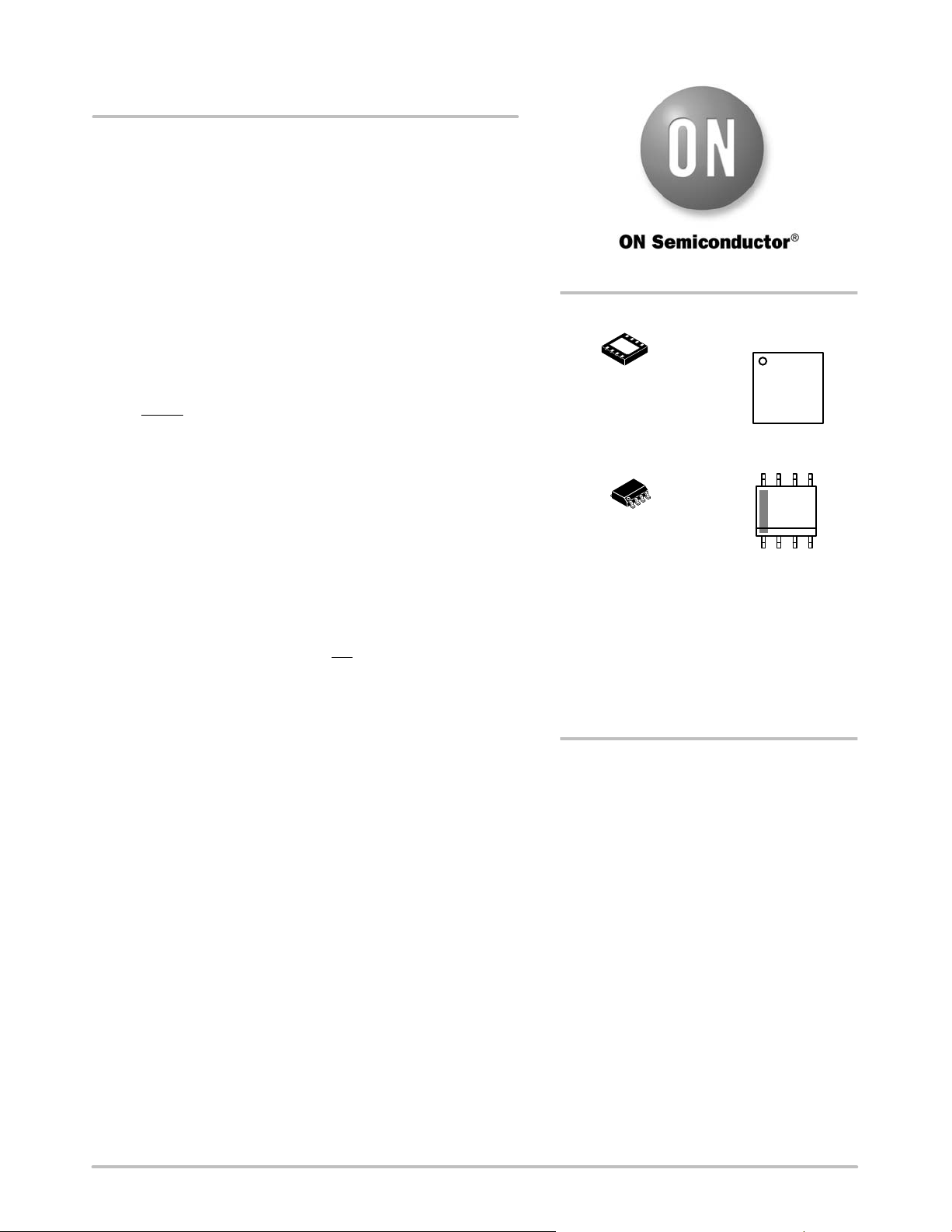
MARKING
DIAGRAMS
1
1
DFN8 3x3
CASE 506BW
8
1
SOIC−8 NB
CASE 751
XXXXX = Specific Device Code
A = Assembly Location
L = Wafer Lot
Y = Year
W = Work Week
G = Pb−Free Package
(Note: Microdot may be in either location)
ORDERING INFORMATION
See detailed ordering and shipping information in the package
dimensions section on page 10 of this data sheet.
XXXXX
XXXXX
ALYWG
G
8
XXXXXX
ALYWX
G
1
© Semiconductor Components Industries, LLC, 2012
February, 2012 − Rev. 8
1 Publication Order Number:
NCP382/D
Page 2
USB INPUT
5V
FLAG1
EN1
FLAG2
EN2
NCP382
IN
Rfault
100 kW
1 mF
FLAG1
EN1
FLAG2
EN2
Figure 1. Typical Application Circuit
OUT1
NCP382
OUT2
GND
120 mF
120 mF
USB
DATA
USB
DATA
D+
D−
VBUS
GND
D+
D−
VBUS
GND
USB
Port
USB
Port
GND
GND
IN
EN1
EN2
1
2
DFN8 SOIC−8
3
4
8
7
6
5
FLAG1
OUT1
OUT2
FLAG2
IN
EN1
EN2
(Top View)
Figure 2. Pin Connections
PIN FUNCTION DESCRIPTION
Pin Name Type Description
EN1 I Enable 1 input, logic low/high (i.e. EN or EN) turns on power switch.
EN2 I Enable 2 input, logic low/high (i.e. EN or EN) turns on power switch.
GND P Ground connection.
IN P
FLAG1 O
FLAG2 O
OUT1 O
OUT2 O
Power−switch input voltage; connect a 1 mF or greater ceramic capacitor from IN to GND as close as possible to
the IC.
Active−low open−drain output 1, asserted during overcurrent or overtemperature conditions. Connect a 10 kW or
greater resistor pull−up, otherwise leave unconnected.
Active−low open−drain output 2, asserted during overcurrent or overtemperature conditions. Connect a 10 kW or
greater resistor pull−up, otherwise leave unconnected.
Power−switch output1; connect a 1 mF ceramic capacitor from OUT1 to GND, as close as possible to the IC.
This minimum value is recommended for USB requirement in terms of load transient response and strong short
circuits.
Power−switch output2; connect a 1 mF ceramic capacitor from OUT2 to GND, as close as possible to the IC.
This minimum value is recommended for USB requirement in terms of load transient response and strong short
circuits.
1
2
3
4
8
FLAG1
7
OUT1
6
OUT2
5
FLAG2
http://onsemi.com
2
Page 3
NCP382
MAXIMUM RATINGS
Rating Symbol Value Unit
From IN to OUT1, From IN to OUT2 Supply Voltage (Note 1) V
IN, OUT1,OUT2, EN1, EN2, FLAG1, FLAG2 (Note 1) V
IN,
FLAG1, FLAG2 sink current I
ESD Withstand Voltage (IEC 61000−4−2) (output only, when
bypassed with 1.0 mF capacitor minimum)
Human Body Model (HBM) ESD Rating are (Note 2) ESD HBM 2000 V
Machine Model (MM) ESD Rating are (Note 2) ESD MM 200 V
Latch−up protection (Note 3)
− Pins IN, OUT1, OUT2, FLAG1
, FLAG2
− EN1, EN2
Maximum Junction Temperature (Note 4) T
Storage Temperature Range T
Moisture Sensitivity (Note 5) MSL Level 1
Stresses exceeding Maximum Ratings may damage the device. Maximum Ratings are stress ratings only. Functional operation above the
Recommended Operating Conditions is not implied. Extended exposure to stresses above the Recommended Operating Conditions may affect
device reliability.
1. According to JEDEC standard JESD22−A108.
2. This device series contains ESD protection and passes the following tests:
Human Body Model (HBM) +/−2.0 kV per JEDEC standard: JESD22−A114 for all pins.
Machine Model (MM) +/−200 V per JEDEC standard: JESD22−A115 for all pins.
3. Latch up Current Maximum Rating: $100 mA per JEDEC standard: JESD78 class II.
4. A thermal shutdown protection avoids irreversible damage on the device due to power dissipation.
5. Moisture Sensitivity Level (MSL): 1 per IPC/JEDEC standard: J−STD−020.
V
IN ,
V
OUT1, VOUT2,
V
FLAG1
OUT1,VOUT2
V
EN1,
, V
FLAG2
SINK
V
EN2,
−7.0 to +7.0 V
−0.3 to +7.0 V
1.0 mA
ESD IEC 15 Air, 8 contact kV
LU
100
J
STG
−40 to + TSD °C
−40 to + 150 °C
mA
OPERATING CONDITIONS
Symbol Parameter Conditions Min Typ Max Unit
V
V
ENX
T
I
SINK
C
C
OUTX
R
q
T
I
OUTX
P
6. A thermal shutdown protection avoids irreversible damage on the device due to power dissipation.
7. The R
final PCB layout.
8. The maximum power dissipation (P
Operational Power Supply 2.5 5.5 V
IN
Enable Voltage 0 5.5
Ambient Temperature Range −40 25 +85 °C
A
FLAG sink current 1 mA
Decoupling input capacitor 1
IN
Decoupling output capacitor USB port per Hub 120
Thermal Resistance Junction−to−Air
JA
DFN−8 package (Notes 6 and 7) 140 °C/W
SOIC−8 package (Notes 6 and 7) 210 °C/W
Junction Temperature Range −40 25 +125 °C
J
Recommended Maximum DC
current
Power Dissipation Rating (Note 8) TA v 25°C
D
DFN−8 package 2 A
SOIC−8 package 1.5 A
DFN−8 package 850 mW
SOIC−8 package 570 mW
TA = 85°C
DFN−8 package 428 mW
SOIC−8 package 285 mW
is dependent of the PCB heat dissipation. Announced thermal resistance is the unless PCB dissipation and can be improve with
q
JA
) is given by the following formula:
D
PD+
T
JMAX
R
qJA
* T
A
mF
mF
http://onsemi.com
3
Page 4
NCP382
ELECTRICAL CHARACTERISTICS Min & Max Limits apply for T
between −40°C to +85°C and TJ up to + 125°C for VIN between
A
2.5 V to 5.5 V (Unless otherwise noted). Typical values are referenced to T
Symbol
Parameter Conditions Min Typ Max Unit
POWER SWITCH
R
DS(on)
R
DS(on)
Static drain−source on−state resistance
(SOIC−8 Package)
Static drain−source on−state resistance
(DFN8 Package)
T
R
Output rise time
TJ = 25°C, VIN = 3.6 V to 5 V 80 11 0
VIN = 5 V –40°C < TJ < 125°C 140
TJ = 25°C, VIN = 3.6 V to 5 V 80 95
VIN = 5 V –40°C < TJ < 125°C 100
VIN = 5 V
VIN = 2.5 V 0.2 0.65 1.0
T
F
Output fall time
VIN = 5 V 0.1 0.5
VIN = 2.5 V 0.1 0.5
ENABLE INPUT ENx OR ENx
High−level input voltage 1.2 V
IH
Low−level input voltage 0.4 V
IL
Input current V
Turn on time
C
LOAD
ENx
= 1 mF, R
Turn off time 1.0 3.0 ms
T
V
V
I
ENx
T
ON
OFF
CURRENT LIMIT
I
OCP
Current−limit threshold (Maximum DC
output current I
delivered to load)
OUTX
VIN = 5 V, Fixed 0.5 A 0.5 0.6 0.7
VIN = 5 V, Fixed 1.0 A 1.0 1.2 1.4
VIN = 5 V, Fixed 1.5 A 1.5 1.75 2.0
VIN = 5 V, Fixed 2 A 2 2.25 2.5
T
T
T
DET
REG
OCP
Response time to short circuit VIN = 5 V 2.0
Regulation time 2.0 3.0 4.0 ms
Over current protection time 14 20 26 ms
UNDERVOLTAGE LOCKOUT
V
UVLO
V
HYST
T
RUVLO
IN pin low−level input voltage VIN rising 2.0 2.35 2.5 V
IN pin hysteresis TJ = 25°C 25 40 60 mV
Re−arming Time VIN rising 5.0 10 15 ms
SUPPLY CURRENT
I
INOFF
I
INON
Low−level output supply current VIN = 5 V, No load on OUTX, Device OFF
V
ENX
High−level output supply current
0.5 A TJ = 25°C
1 and 1.5 A TJ = 25°C
2 A TJ = 25°C
I
REV
Reverse leakage current V
OUTX
V
IN
= 5 V,
= 0 V
FLAG PIN
V
I
LEAK
T
T
FOCP
OL
FLG
FLAGX output low voltage I
Off−state leakage V
FLAGX deglitch FLAGX de−assertion time due to
FLAGX deglitch FLAGX assertion due to overcurrent 6 8 12 ms
THERMAL SHUTDOWN
T
SD
T
SDOCP
T
RSD
9. Parameters are guaranteed for C
10.DFN package only.
Thermal shutdown threshold 140 °C
Thermal regulation threshold 125 °C
Thermal regulation rearming threshold 115 °C
LOAD
and R
connected to the OUTX pin with respect to the ground.
LOAD
11.Guaranteed by characterization.
= + 25°C and VIN = 5 V.
A
R
LOAD
= 0 V, V
LOAD
C
= 1 mF,
LOAD
= 100 W (Note 9)
= 5 V −0.5 0.5
ENx
= 100 W (Note 9)
0.3 1.0 1.5
1.0 3.0 ms
2.0 3.0
= 0 V or V
ENX
T
T
T
J
J
J
= 5 V
= 85°C
= 85°C
= 85°C
TJ = 25°C 1.0 2.0
= 1 mA 400 mV
FLAGX
= 5 V 0.02 1
FLAGX
4 6 9 ms
overcurrent
95
100
115
125
130
140
mW
mW
ms
mA
A
ms
mA
mA
mA
mA
http://onsemi.com
4
Page 5

VIN
NCP382
IN OUT1
mF
1
NCP382
OUT2
CLOAD
RLOAD
VENx
VENx
VOUTx
TON
50%
90%
GND
TOFF
10%
Figure 4. Voltage Waveform
CLOAD RLOAD
Figure 3. Test Configuration
TR TF
VOUTx
90%
10%
10%
http://onsemi.com
5
Page 6

NCP382
BLOCK DIAGRAM
EN1
GND
IN
EN block
Current
Limiter
Oscilator
V
UVLO
TSD
Current
Limiter
REF
Control logic
and timer
Gate Driver
Blocking control
Blocking control
Gate Driver
Flag
Channel 1
Channel 2
Flag
/FLAG 1
OUT 1
OUT 2
/FLAG 2
EN2
EN block
Control logic
and timer
Figure 5. Block Diagram
http://onsemi.com
6
Page 7

NCP382
FUNCTIONAL DESCRIPTION
Overview
The NCP382 is a dual high side power distribution
switches designed to protect the input supply voltage in case
of heavy capacitive loads, short circuit or over current. In
addition, the high side MOSFETs are turned off during
undervoltage or thermal shutdown condition. Thanks to the
soft start circuitry, NCP382 is able to limit large current and
voltage surges.
Overcurrent Protection
NCP382 switches into a constant current regulation mode
when the output current is above the I
threshold.
OCP
Depending on the load, the output voltage is decreased
accordingly.
− In case of hot plug with heavy capacitive load, the
output voltage is brought down to the capacitor voltage.
The NCP382 will limit the current to the I
OCP
threshold
value until the charge of the capacitor is completed.
VOUTX
Drop due to
capacitor charge
IOUTX
IOCP
VOUTX
Thermal
Regulation
Threshold
Timer
Regulation
Mode
IOUTX
IOCP
TREGTOCP
Figure 8. Short−Circuit
Then, the device enters in timer regulation mode, described
in 2 phases:
− Off−phase: Power MOSFET is off during T
the die temperature to drop.
− On−phase: regulation current mode during T
current is regulated to the I
OCP
level.
The timer regulation mode allows the device to handle
high thermal dissipation (in case of short circuit for
example) within temperature operating condition.
NCP382 stays in on−phase/off−phase loop until the over
current condition is removed or enable pin is toggled.
Remark: other regulation modes can be available for
different applications. Please contact our On Semiconductor
representative for availability.
OCP
REG.
to allow
The
Figure 6. Heavy Capacitive Load
− In case of overload, the current is limited to the I
value and the voltage value is reduced according to the
load by the following relation:
V
OUTX
+ R
LOAD2
I
OCP
VOUTX
IOCP x RLOAD
IOUTX
IOCP
Figure 7. Overload
− In case of short circuit or huge load, the current is
limited to the I
value within T
OCP
time until the
DET
short condition is removed. If the output remains
shorted or tied to a very low voltage, the junction
temperature of the chip exceeds T
SDOCP
value and the
device enters in thermal shutdown (MOSFET is
turned−off).
OCP
(eq. 1)
FLAG Indicator
The FLAG pin is an open−drain MOSFET asserted low
during overcurrent or overtemperature conditions. When an
overcurrent fault is detected on the power path, FLAG
pin
is asserted low at the end of the associate deglitch time
(TFOCP). Thanks to this feature, the FLAG
pin is not tied
low during the charge of a heavy capacitive load or a voltage
transient on output. The FLAG
fault is removed. Then, the FLAG
of T
FGL
Undervoltage Lock−out
pin remains low until the
pin goes high at the end
Thanks to a built−in under voltage lockout (UVLO)
circuitry, the output remains disconnected from input until
V
voltage is above V
IN
. This circuit has a V
UVLO
HYST
hysteresis witch provides noise immunity to transient
condition.
Thermal Sense
Thermal shutdown turns off the power MOSFET if the die
temperature exceeds T
. A built-in hysteresis prevents the
SD
part from turning on until the die temperature cools at
TRSD.
http://onsemi.com
7
Page 8

NCP382
Enable Input
Enable pin must be driven by a logic signal (CMOS or
TTL compatible) or connected to the GND or VIN. A logic
low on ENX
high on ENX
the current consumption down to I
Blocking Control
or high on ENX turns−on the device. A logic
or low on ENX turns off device and reduces
.
INOFF
The blocking control circuitry switches the bulk of the
power MOS. When the part is off, the body diode limits the
APPLICATION INFORMATION
Power Dissipation
The junction temperature of the device depends on
different contributing factors such as board layout, ambient
temperature, device environment, etc... Yet, the main
contributor in term of junction temperature is the power
dissipation of the power MOSFET. Assuming this, the
power dissipation and the junction temperature in normal
mode can be calculated with the following equations:
2
ǒ
I
OUT1
qJA
Ǔ
) T
)ǒI
PD+ R
P
D
R
I
T
R
T
= Power MOSFET on resistance (W)
DS(on)
= Output current in channel X (A)
OUTx
J
= Package thermal resistance (°C/W)
JA
q
A
DS(on)
= Power dissipation (W)
TJ+ PD R
= Junction temperature (°C)
= Ambient temperature (°C)
ǒ
A
OUT2
2
Ǔ
Ǔ (eq. 2)
(eq. 3)
leakage current I
from OUTX to IN. In this mode, anode
REV
of the body diode is connected to IN pin and cathode is
connected to OUTX pin. In operating condition, anode of
the body diode is connected to OUTX pin and cathode is
connected to IN pin preventing the discharge of the power
supply.
Power dissipation in regulation mode can be calculated by
taking into account the drop V
IN
−V
link to the load by
OUTX
the following relation:
PD+
ǒ
ǒ
VIN* R
I
OCP
LOAD1
I
OCP
Ǔ)ǒ
VIN* R
LOAD2
I
OCP
(eq. 4)
Ǔ
Ǔ
PD = Power dissipation (W)
V
IN
R
LOADX
I
= Output regulated current (A)
OCP
PCB Recommendations
= Input Voltage (V)
= Load Resistance on channel X (W)
The NCP382 integrates two PMOS FET rated up to 2 A,
and the PCB design rules must be respected to properly
evacuate the heat out of the silicon. The DFN8 PAD1 must
be connected to ground plane to increase the heat transfer if
necessary. Of course, in any case, this pad must not connect
to any other potential. By increasing PCB area, the R
of
JA
q
the package can be decreased, allowing higher current.
http://onsemi.com
8
Page 9

NCP382
Figure 9. USB Host Typical Application
http://onsemi.com
9
Page 10

NCP382
ORDERING INFORMATION
Active
Enable
Device Marking
NCP382LMN05AATXG
NCP382LMN10AATXG
NCP382LMN15AATXG
NCP382LMN20AATXG
NCP382HMN05AATXG
NCP382HMN10AATXG
NCP382HMN15AATXG
NCP382HMN20AATXG
NCP382LD05AA
R2G
NCP382LD10AA
R2G
NCP382LD15AA
R2G
NCP382HD05AA
R2G
NCP382HD10AA
R2G
NCP382HD15AA
R2G
†For information on tape and reel specifications, including part orientation and tape sizes, please refer to our Tape and Reel Packaging
Specifications Brochure, BRD8011/D.
382
L05
382
L10
382
L15
382
L20
382
H05
382
H10
382
H15
382
H20
382L05
382L10 1.0 A NCP382LD
382L15 1.5 A NCP382LD
382H05
382H10 1.0 A NCP382HD
382H15 1.5 A NCP382HD
Level
ENx
Low
ENx
High
ENx
Low
ENx
High
Over
Current
Limit
0.5 A NCP382LM
1.0 A NCP382LM
1.5 A NCP382LM
2.0 A NCP382LM
0.5 A NCP382HM
1.0 A NCP382HM
1.5 A NCP382HM
2.0 A NCP382HM
0.5 A NCP382LD
0.5 A NCP382HD
Evaluation
Board
N05AGEVB
N10AGEVB
N15AGEVB
N20AGEVB
N05AGEVB
N10AGEVB
N15AGEVB
N20AGEVB
05AAGEVB
10AAGEVB
15AAGEVB
05AAGEVB
10AAGEVB
15AAGEVB
2367
IEC6095
UL
N N N
N N N
N N N
N N N
N N N
N N N
N N N
N N N
Y Y Y
Y Y Y
Y Y Y
Y Y Y
Y Y Y
Y Y Y
0 Ed2
(CB
Scheme)
IEC6095
0 Ed2
Ad1
Package Shipping
DFN8
(Pb−Free)
SOIC−8
(Pb−Free)
3000 /
Tape / Reel
2500 /
Tape / Reel
†
http://onsemi.com
10
Page 11

NCP382
ÉÉÉ
ÉÉÉ
PACKAGE DIMENSIONS
DFN8, 3x3, 0.65P
CASE 506BW
ISSUE O
PIN ONE
REFERENCE
2X
0.10 C
2X
0.05 C
0.05 C
NOTE 4
8X
0.10 C
DETAIL A
L
D
A
B
E
TOP VIEW
DETAIL B
SIDE VIEW
(A3)
A1
D2
14
E2
A
C
L1
SEATING
PLANE
L
DETAIL A
OPTIONAL
CONSTRUCTIONS
MOLD CMPDEXPOSED Cu
DETAIL B
OPTIONAL
CONSTRUCTIONS
NOTES:
L
1. DIMENSIONING AND TOLERANCING PER
ASME Y14.5M, 1994.
2. CONTROLLING DIMENSION: MILLIMETERS.
3. DIMENSION b APPLIES TO PLATED TERMINAL
AND IS MEASURED BETWEEN 0.15 AND
0.30mm FROM THE TERMINAL TIP.
4. COPLANARITY APPLIES TO THE EXPOSED
PAD AS WELL AS THE TERMINALS.
MILLIMETERS
DIM MIN MAX
A 0.80 1.00
A1 0.00 0.05
A3 0.20 REF
b 0.25 0.35
D 3.00 BSC
D2 2.30 2.50
E 3.00 BSC
E2 1.55 1.75
e 0.65 BSC
K 0.20 −−−
L 0.35 0.45
L1 0.00 0.15
RECOMMENDED
SOLDERING FOOTPRINT*
2.50
1.75
8X
0.62
3.30
8X
K
e/2
e
BOTTOM VIEW
58
8X
b
0.10 B
0.05ACC
NOTE 3
0.65
PITCH
1
DIMENSIONS: MILLIMETERS
8X
0.40
*For additional information on our Pb−Free strategy and soldering
details, please download the ON Semiconductor Soldering and
Mounting Techniques Reference Manual, SOLDERRM/D.
http://onsemi.com
11
Page 12

−Y−
−Z−
NCP382
PACKAGE DIMENSIONS
SOIC−8 NB
CASE 751−07
ISSUE AK
NOTES:
−X−
A
58
B
1
S
0.25 (0.010)
4
M
M
Y
K
G
C
SEATING
PLANE
0.10 (0.004)
H
D
0.25 (0.010) Z
M
Y
SXS
N
X 45
_
M
J
SOLDERING FOOTPRINT*
1. DIMENSIONING AND TOLERANCING PER
ANSI Y14.5M, 1982.
2. CONTROLLING DIMENSION: MILLIMETER.
3. DIMENSION A AND B DO NOT INCLUDE
MOLD PROTRUSION.
4. MAXIMUM MOLD PROTRUSION 0.15 (0.006)
PER SIDE.
5. DIMENSION D DOES NOT INCLUDE DAMBAR
PROTRUSION. ALLOWABLE DAMBAR
PROTRUSION SHALL BE 0.127 (0.005) TOTAL
IN EXCESS OF THE D DIMENSION AT
MAXIMUM MATERIAL CONDITION.
6. 751−01 THRU 751−06 ARE OBSOLETE. NEW
STANDARD IS 751−07.
MILLIMETERS
DIMAMIN MAX MIN MAX
4.80 5.00 0.189 0.197
B 3.80 4.00 0.150 0.157
C 1.35 1.75 0.053 0.069
D 0.33 0.51 0.013 0.020
G 1.27 BSC 0.050 BSC
H 0.10 0.25 0.004 0.010
J 0.19 0.25 0.007 0.010
K 0.40 1.27 0.016 0.050
M 0 8 0 8
____
N 0.25 0.50 0.010 0.020
S 5.80 6.20 0.228 0.244
INCHES
1.52
0.060
7.0
0.275
0.6
0.024
4.0
0.155
1.270
0.050
SCALE 6:1
ǒ
inches
mm
Ǔ
*For additional information on our Pb−Free strategy and soldering
details, please download the ON Semiconductor Soldering and
Mounting Techniques Reference Manual, SOLDERRM/D.
ON Semiconductor and are registered trademarks of Semiconductor Components Industries, LLC (SCILLC). SCILLC reserves the right to make changes without further notice
to any products herein. SCILLC makes no warranty, representation or guarantee regarding the suitability of its products for any particular purpose, nor does SCILLC assume any liability
arising out of the application or use of any product or circuit, and specifically disclaims any and all liability, including without limitation special, consequential or incidental damages.
“Typical” parameters which may be provided in SCILLC data sheets and/or specifications can and do vary in different applications and actual performance may vary over time. All
operating parameters, including “Typicals” must be validated for each customer application by customer’s technical experts. SCILLC does not convey any license under its patent rights
nor the rights of others. SCILLC products are not designed, intended, or authorized for use as components in systems intended for surgical implant into the body, or other applications
intended to support or sustain life, or for any other application in which the failure of the SCILLC product could create a situation where personal injury or death may occur. Should
Buyer purchase or use SCILLC products for any such unintended or unauthorized application, Buyer shall indemnify and hold SCILLC and its officers, employees, subsidiaries, affiliates,
and distributors harmless against all claims, costs, damages, and expenses, and reasonable attorney fees arising out of, directly or indirectly, any claim of personal injury or death
associated with such unintended or unauthorized use, even if such claim alleges that SCILLC was negligent regarding the design or manufacture of the part. SCILLC is an Equal
Opportunity/Affirmative Action Employer. This literature is subject to all applicable copyright laws and is not for resale in any manner.
PUBLICATION ORDERING INFORMATION
LITERATURE FULFILLMENT:
Literature Distribution Center for ON Semiconductor
P.O. Box 5163, Denver, Colorado 80217 USA
Phone: 303−675−2175 or 800−344−3860 Toll Free USA/Canada
Fax: 303−675−2176 or 800−344−3867 Toll Free USA/Canada
Email: orderlit@onsemi.com
N. American Technical Support: 800−282−9855 Toll Free
USA/Canada
Europe, Middle East and Africa Technical Support:
Phone: 421 33 790 2910
Japan Customer Focus Center
Phone: 81−3−5817−1050
http://onsemi.com
12
ON Semiconductor Website: www.onsemi.com
Order Literature: http://www.onsemi.com/orderlit
For additional information, please contact your local
Sales Representative
NCP382/D
Page 13

 Loading...