

Datasheet NCP367DPMEBTBG, NCP367DPMUECTBG, NCP367DPMUEETBG, NCP367DPMUELTBG, NCP367OPMUEATBG Datasheet (ON) [ru]
...
NCP367
Battery Charge Front-End
Protection, USB and AC/DC
Supply Compliant
NCP367 is a charge path protection device which allows
disconnecting the systems from its output pin in case wrong charging
conditions are detected. The system is positive overvoltage protected
up to +30 V. Thanks to a very low current consumption, the USB
charge is compatible with this integrated component.
This device uses internal PMOS FET, making external devices
unnecessary, which reduces the system cost and PCB area of the
application board. First, NCP367 is able to instantaneously
disconnect the output from the input if the input voltage exceeds the
overvoltage threshold. Additional overcurrent protection function
allows turning off internal PMOS FET when the charge current
exceeds current limit, which is externally selectable.
The current limit value can be modified with control logic pin to
divide it by internal gain, allowing USB 100 mA/500 mA charging or
USB/Wall adapter charging up to overcurrent threshold. At the same
time, Li ion Battery voltage is continuously monitored, providing
more safety during the charge. Thermal shutdown protection is also
available.
NCP367 provides a negative going flag (FLAG) output, which
alerts the system that a fault has occurred as overvoltage (power
supply or battery voltage), overcurrent or thermal event.
In addition, the device has ESD−protected input (15 kV Air) when
bypassed with a 1 mF or larger capacitor.
Features
• Overvoltage Protection Up to + 30 V
• Fast Turn Off Time
• Very Low Current Consumption/USB Compliant
• Li ion Battery Voltage Monitoring
• Overvoltage Lockout (OVLO)
• Undervoltage Lockout (UVLO)
• Overcurrent Protection Externally Adjustable (OCP) up to 2.8 A
• Thermal Shutdown
• Shutdown EN and Gain Input Pins
• Soft−Start to Eliminate Inrush Current
• Alert FLAG Output
• Compliance to IEC61000−4−2 (Level 4)
8 kV (Contact), 15 kV (Air)
• ESD Ratings: Machine Model = B
ESD Ratings: Human Body Model = 2
• 8 Lead DFN 2.2x2 mm Package
• These are Pb−Free Devices
T ypical Application
• USB Devices
• Mobile Phones
• Peripheral
• Personal Digital Applications
• MP3 Players
www.onsemi.com
8
1
DFN8
MU SUFFIX
CASE 506BP
MARKING DIAGRAM
1
XX MG
G
XX = Specific Device Code
M = Date Code
G = Pb−Free Device
(Note: Microdot may be in either location)
PIN ASSIGNMENT
IN
1
2
VBAT
NC
ILIM
ORDERING INFORMATION
See detailed ordering, marking and shipping information in the
package dimensions section on page 12 of this data sheet.
OUT
3
4
(Top View)
8
7
6
5
GND
FLAG
GS
EN
© Semiconductor Components Industries, LLC, 2015
February, 2015 − Rev . 11
1 Publication Order Number:
NCP367/D
NCP367
Wall Adapter / USB
1 mF
VIN/VUSB
ILIM
GS
NCP367
MCU
1
IN
5
EN
6
GS
GND
8
OUT
FLAG
VBAT
ILIM
9
7
2
4
DCDC
Figure 1. Typical Application Circuit
I limit
+
GAIN
1/2.75
LDO
1 mF
Soft−Start
Driver
B+
Battery Charger
10 k
100 k
Li+
BATTERY
OUT
VBAT
4.35 V
VREF
OVLO
UVLO
GND
EN Pin
Figure 2. Functional Block Diagram
Logic
+
Timer
Thermal
Shutdown
FLAG
www.onsemi.com
2
NCP367
PIN FUNCTION DESCRIPTION
Pin Name Type Description
1 IN POWER Input Voltage Pin. This pin is connected to the power supply: W all Adapter or USB. A 1 mF low ESR
2
V
BAT
INPUT
3 NC OUTPUT Not Connected
4
I
LIM
OUTPUT
5 EN INPUT Enable Mode Pin. The device enters in shutdown mode when this pin is tied to a high level. In this case
6 GS INPUT Gain Select Pin. When the GS pin is tied to 0 level, the Overcurrent threshold is defined by Ilimit set-
7 FLAG OUTPUT Fault Indication Pin. This pin allows an external system to detect fault condition. The FLAG pin goes
8 GND POWER Ground.
9 OUT OUTPUT Output Voltage Pin. This pin follows IN pin when “no input fault” is detected. The output is disconnected
ceramic capacitor, or larger, must be connected between this pin and GND.
Li ion Battery voltage sense pin. A serial resistor must be placed between this pin and positive pin of
the battery pack.
Current Limit Pin. This pin provides the reference, based on the internal band−gap voltage reference, to
limit the overcurrent, across internal PMOSFET, from IN to OUT. A 1% tolerance, or better, resistor
shall be used to get the highest accuracy of the Overcurrent Limit.
the output is disconnected from the input. The state of this pin does not have an impact on the fault
detection of the FLAG pin.
ting. See logic table. When GS pin is tied to high, the Overcurrent threshold is set to Ilimit/GS
low when input voltage is below UVLO threshold, exceeds OVLO threshold, charge current from wall
adapter to battery exceeds programmed current limit, Li ion Battery voltage (4.3 V) is exceeded or internal temperature exceeds thermal shutdown limit. Since the FLAG pin is open drain functionality, an
external pull−up resistor to VBattery must be added (10 kW minimum value).
from the Vin power supply when voltage, current or thermal fault events are detected. A 1 mF low ESR
ceramic capacitor, or larger, must be connected between this pin and GND.
NOTE: Pin out provided for concept purpose only and might change in the final product
MAXIMUM RATINGS
Rating Symbol Value Unit
Minimum Voltage (IN to GND) Vmin
in
Minimum Voltage (All others to GND) Vmin −0.3 V
Maximum Voltage (IN to GND) Vmax
in
Maximum Voltage (All others to GND) Vmax 7.0 V
Maximum DC Current from Vin to V out (PMOS) Imax 3.4 A
Thermal Resistance, Junction−to−Air (without PCB area) R
Operating Ambient Temperature Range T
Storage Temperature Range T
Junction Operating Temperature T
ESD Withstand Voltage (IEC 61000−4−2)
q
JA
A
stg
J
Vesd 15 Air, 8.0 Contact
Human Body Model (HBM), Model = 2 (Note 1)
Machine Model (MM) Model = B (Note 2)
Latchup LU Class 1 −
Moisture Sensitivity MSL Level 1 −
Stresses exceeding those listed in the Maximum Ratings table may damage the device. If any of these limits are exceeded, device functionality
should not be assumed, damage may occur and reliability may be affected.
1. Human Body Model, 100 pF discharged through a 1.5 kW resistor following specification JESD22/A114.
2. Machine Model, 200 pF discharged through all pins following specification JESD22/A115.
−0.3 V
30 V
190 °C/W
−40 to +85 °C
−65 to +150 °C
150 °C
kV
2000
200
V
V
www.onsemi.com
3
NCP367
FLAG Output Low Voltage
FLAG Leakage Current
EN Leakage Current
FLAG going up Delay
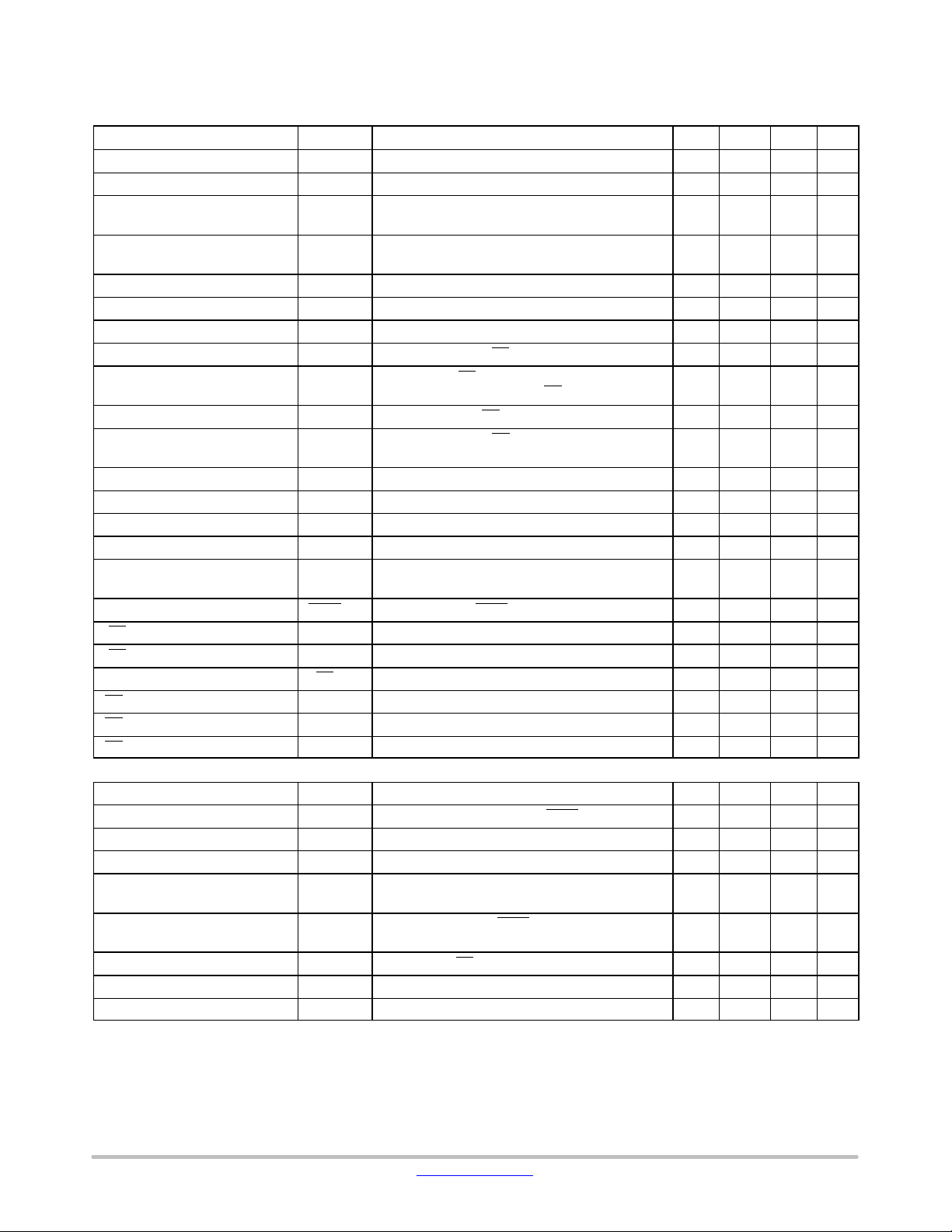
ELECTRICAL CHARACTERISTICS − NCP367OPMUEA
(Min/Max limits values (−40°C < T
Characteristic Symbol Conditions Min Typ Max Unit
Input Voltage Range V
Undervoltage Lockout Threshold UVLO Vin falls down UVLO threshold 1.75 1.85 1.9 V
Undervoltage Lockout
Hysteresis
Overvoltage Lockout Threshold
NCP367OPMUEA
Overvoltage Lockout Hysteresis OVLO
Vin versus Vout Resistance R
Supply Quiescent Current Idd No Load 42 130 mA
Disable Mode Idd
Overcurrent Threshold
NCP367OPMUEA
Overcurrent Response I
Current Limit Gain
NCP367OPMUEA
Battery Overvoltage Threshold OV
Battery Overvoltage Hysteresis OV
V
Pin Leakage VBAT
BAT
V
Deglitch Time VBAT
BAT
EN Voltage High V
EN Voltage Low V
GS Voltage High V
GS Voltage Low V
GS Leakage Current GS
TIMINGS
Start Up Delay t
Rearming Delay t
Overcurrent Regulation Time t
Output Turn Off T ime t
Alert Delay t
Disable Time t
Thermal Shutdown Temperature T
Thermal Shutdown Hysteresis Tsd
NOTE: Electrical parameters are guaranteed by correlation across the full range of temperature.
< +85°C) and Vin = +3.5 V . Typical values are TA = +25°C, unless otherwise noted.)
A
1.2 28 V
UVLO
in
hyst
OVLO Vin rises up OVLO threshold
3.65 3.8 3.95
hyst
Enable Mode, Load Connected to V
out
EN = 1.2 V 35 110 mA
EN = low, Load Connected to V
R
= 0 W, 1 A/ms, GS = 0.4 V 2.30 2.85 3.40
ilim
1 A/ms, GS = low, I
= 1.51 A 5.0 %
lim
out
,,
GS = 1.2 V
0°C to 85°C 4.3 4.35 4.4 V
0°C to 85°C 100 150 200 mV
V
BAT
> OV
BAT
0.2 2.0 4.0 ms
Vin > OVLO
I
GS
Vol
DS(on)
dis
OCP
reg
value
BAT
HYS
LEAK
DEG
flag
Sink 1 mA on FLAG pin
FLAG
EN
t
start
REARM
REG
ih
leak
ih
leak
on
off
leak
il
il
From Vin > UVLO to V
From V
From Vin > OVLO to V
FLAG level = 5 V 10 nA
1.2 V
1.2 V
= 0.8xV
out
> 0.2xVin to FLAG = 1.2 V 15 30 45 ms
out
in
15 30 45 ms
OCP Active 15 30 45 ms
OCP Active 1.2 1.8 3.0 ms
≤ 0.3 V, Vin increasing
out
from 3.5 V to 6.5 V at 3 V/ms.
stop
From Vin > OVLO to FLAG ≤ 0.4 V, (see Figure 16)
Vin increasing from 3.5 V to 6.5 V at 3 V/ms
dis
From EN 0.4 to 1.2 V to V
sd
hyst
≤ 0.3 V 3.0 ms
out
60 100 mV
45 150 mV
50 100 mW
2.55
20 nA
400 mV
0.4 V
200 nA
0.4 V
200 nA
1.5 5.0 ms
1.5 ms
150 °C
30 °C
V
A
www.onsemi.com
4
NCP367
FLAG Output Low Voltage
FLAG Leakage Current
EN Leakage Current
FLAG going up Delay
ELECTRICAL CHARACTERISTICS − NCP367DPMUEB
(Min/Max limits values (−40°C < T
Characteristic Symbol Conditions Min Typ Max Unit
Input Voltage Range V
Undervoltage Lockout Threshold UVLO Vin falls down UVLO threshold 1.75 1.85 1.9 V
Undervoltage Lockout
Hysteresis
Overvoltage Lockout Threshold
NCP367DPMUEB
Overvoltage Lockout Hysteresis OVLO
Vin versus Vout Resistance R
Supply Quiescent Current Idd No Load 42 130 mA
Disable Mode Idd
Overcurrent Threshold
NCP367DPMUEB
Overcurrent Response I
Current Limit Gain
NCP367DPMUEB
Battery Overvoltage Threshold OV
Battery Overvoltage Hysteresis OV
V
Pin Leakage VBAT
BAT
V
Deglitch Time VBAT
BAT
EN Voltage High V
EN Voltage Low V
GS Voltage High V
GS Voltage Low V
GS Leakage Current GS
TIMINGS
Start Up Delay t
Rearming Delay t
Overcurrent Regulation Time t
Output Turn Off T ime t
Alert Delay t
Disable Time t
Thermal Shutdown Temperature T
Thermal Shutdown Hysteresis Tsd
NOTE: Electrical parameters are guaranteed by correlation across the full range of temperature.
< +85°C) and Vin = +4.0 V . Typical values are TA = +25°C, unless otherwise noted.)
A
1.2 28 V
UVLO
in
hyst
OVLO Vin rises up OVLO threshold
4.38 4.54 4.7
hyst
Vin = 5 V , Enable Mode, Load Connected to V
EN = 1.2 V 35 110 mA
Vin = 4.3 V , EN = low, Load Connected to V
R
= 0 W, 1 A/ms, GS = 0.4 V 1.25 1.45 1.80
ilim
1 A/ms, GS = low, I
= 1.51 A 5.0 %
lim
GS = 1.2 V
Vin = 4.2 V , 0°C to 85°C 4.3 4.35 4.4 V
Vin = 4.2 V , 0°C to 85°C 100 160 200 mV
Vin = 4.0 V , 20 nA
V
> OV
BAT
BAT
Vin > OVLO
out
out
,,
0.2 2.0 4.0 ms
I
GS
Vol
DS(on)
dis
OCP
reg
value
BAT
HYS
LEAK
DEG
flag
Sink 1 mA on FLAG pin
FLAG
EN
t
start
REARM
REG
ih
leak
ih
leak
on
off
leak
il
il
From Vin > UVLO to V
From V
From Vin > OVLO to V
FLAG level = 5 V 10 nA
1.2 V
1.2 V
= 0.8xV
out
> 0.2xVin to FLAG = 1.2 V 15 30 45 ms
out
in
15 30 45 ms
OCP Active 15 30 45 ms
OCP Active 1.2 1.8 3.0 ms
≤ 0.3 V, Vin increasing
out
from 4 V to 7 V at 3 V/ms.
stop
From Vin > OVLO to FLAG ≤ 0.4 V, (see Figure 16)
Vin increasing from 4 V to 7 V at 3 V/ms
dis
From EN 0.4 to 1.2 V to V
sd
hyst
≤ 0.3 V 3.0 ms
out
60 100 mV
45 100 mV
50 100 mW
2.77
400 mV
0.4 V
200 nA
0.4 V
200 nA
1.5 5.0 ms
1.5 ms
150 °C
30 °C
V
A
www.onsemi.com
5

NCP367
Current Limit Gain NCP367Dx
Ox
FLAG Output Low Voltage
FLAG Leakage Current
EN Leakage Current
FLAG going up Delay
ELECTRICAL CHARACTERISTICS − Other OVLO version
(Min/Max limits values (−40°C < T
Characteristic Symbol Conditions Min Typ Max Unit
Input Voltage Range V
Undervoltage Lockout Threshold UVLO Vin falls down UVLO threshold 1.75 1.85 1.9 V
Undervoltage Lockout
Hysteresis
Overvoltage Lockout Threshold
NCP367xPMUEC
NCP367DPMUEE
NCP367DPMUEL
NCP367OPMUEO
Overvoltage Lockout Hysteresis OVLO
Vin versus Vout Resistance R
Supply Quiescent Current Idd No Load 42 130 mA
Disable Mode Idd
Overcurrent Threshold
NCP367Dx
NCP367Ox
Overcurrent Response I
NCP367
Battery Overvoltage Threshold OV
Battery Overvoltage Hysteresis OV
V
Pin Leakage VBAT
BAT
V
Deglitch Time VBAT
BAT
EN Voltage High V
EN Voltage Low V
GS Voltage High V
GS Voltage Low V
GS Leakage Current GS
TIMINGS
Start Up Delay t
Rearming Delay t
Overcurrent Regulation Time t
Output Turn Off T ime t
Alert Delay t
Disable Time t
Thermal Shutdown Temperature T
Thermal Shutdown Hysteresis Tsd
NOTE: Electrical parameters are guaranteed by correlation across the full range of temperature.
< +85°C) and Vin = +5.0 V . Typical values are TA = +25°C, unless otherwise noted.)
A
1.2 28 V
UVLO
in
hyst
OVLO Vin rises up OVLO threshold
5.64
5.85
6.60
6.90
hyst
DS(on)
dis
I
OCP
Vin = 5 V , Enable Mode, Load Connected to V
EN = 1.2 V 40 110 mA
Vin = 5 V , EN = low, Load Connected to V
R
= 0 W, 1 A/ms, GS = 0.4 V 1.25
ilim
out
out
,,
2.30
GS
Vol
reg
value
BAT
HYS
LEAK
flag
DEG
1 A/ms, GS = low, I
GS = 1.2 V 2.70
0°C to 85°C 4.3 4.35 4.4 V
0°C to 85°C 100 150 200 mV
V
BAT
Vin > OVLO
= 1.51 A 5.0 %
lim
> OV
BAT
0.2 2.0 4.0 ms
Sink 1 mA on FLAG pin
FLAG
EN
t
start
REARM
REG
ih
leak
ih
leak
on
off
leak
il
il
From Vin > UVLO to V
From V
From Vin > OVLO to V
FLAG level = 5 V 10 nA
Vin from 3.3 V to 5.25 V 1.2 V
Vin from 3.3 V to 5.25 V 0.4 V
EN = 5.5 V or GND 200 nA
Vin from 3.3 V to 5.25 V 1.2 V
Vin from 3.3 V to 5.25 V 0.4 V
EN = 5.5 V or GND 200 nA
= 0.8xV
out
> 0.2xVin to FLAG = 1.2 V 15 30 45 ms
out
in
15 30 45 ms
OCP Active 15 30 45 ms
OCP Active 1.2 1.8 3.0 ms
≤ 0.3 V, Vin increasing
out
from 5 V to 8 V at 3 V/ms.
stop
From Vin > OVLO to FLAG ≤ 0.4 V, (see Figure 16)
Vin increasing from 5 V to 8 V at 3 V/ms
dis
From EN 0.4 to 1.2 V to V
sd
hyst
≤ 0.3 V 3.0 ms
out
80 100 mV
5.85
6.07
6.84
7.20
6.05
6.28
7.08
7.50
100 150 mV
50 100 mW
1.51
2.85
1.80
3.40
2.55
20 nA
400 mV
1.5 5.0 ms
1.5 ms
150 °C
30 °C
V
A
www.onsemi.com
6

NCP367
TYPICAL OPERATING CHARACTERISTICS
Vin
V
in
V
in
V
in
t
on
t
start
/FLAG
/FLAG
Figure 3. Hot Plug−in from 0 to 5 V,
and t
t
t
V
t
on
start
on
in
start
V
out
/Flag
Vout
V
/FLAG
/FLAG
t
stop
t
off
Figure 4. Overvoltage from 5 to 8 V,
and t
t
Vin
off
V
Vin
in
V
Vout /Flag
Vout
/Flag
out
stop
out
Figure 5. Retrieve Normal Operation,
and t
t
on
start
V
in
/Flag
Figure 7. Battery Overvoltage, Deglitch Time
VBat
DEG
V
bat
www.onsemi.com
7
Figure 6. Overvoltage from 0 to 10 V
V
out

NCP367
TYPICAL OPERATING CHARACTERISTICS
2.00
1.98
1.96
1.94
1.92
1.90
1.88
UVLO (V)
1.86
1.84
1.82
1.80
4.40
4.35
4.30
(V)
4.25
BAT
OV
4.20
4.15
5.66
5.64
UVLO + hysteresis
UVLO
0−50 50 100 125
25−25 75 25−25 75
TEMPERATURE (°C)
5.62
5.60
5.58
OVLO (V)
5.56
5.54
5.52
5.50
0−50 50 100 125
TEMPERATURE (°C)
OVLO
OVLO − Hysteresis
Figure 8. UVLO and Hysteresis Figure 9. OVLO and Hysteresis vs. Temperature
(5.6 V version)
20
15
(nA)
10
LEAK
VBAT
5
4.10
Figure 10. V
0−50 50 100 125
25−25 75 25−25 75
TEMPERATURE (°C)
Threshold and Hysteresis vs.
BAT
0
Figure 11. V
0−50 50 100 125
TEMPERATURE (°C)
Pin Leakage vs. Temperature
BAT
Temperature
www.onsemi.com
8

NCP367
APPLICATION INFORMATION
Operation
The NCP367 is an integrated IC which offers a complete
protection of the portable devices during the Li ion battery
charge.
First, the input pin is protected up to +30 V, protecting
the down stream system (charger, transceiver, system...)
against the power supply transients such as inrush current
or defective functionality. Additional protection level is
offered with the overcurrent block which eliminates
current peak or opens the charge path if an overcurrent
default appears.
More of that, the battery voltage is monitored all along
the input power supply is connected, allowing to open
charge path if Li ion battery voltage exceeds 4.3 V, caused
by CCCV charger or battery pack fault.
The integrated pass element (PMOS FET) is sized to
support very high charge DC current up to 2.3 A. The
overcurrent threshold can be externally adjusted with a
pull−down resistor and gain select pin is available to divide
current limit threshold with internal fixed gain. Allowing
to adjust with logic pin the overcurrent threshold if
USB/500 mA or WA/1.5 A is detected, without changing
R
resistor, in example.
ILIM
Undervoltage, Overvoltage, Overcurrent and thermal
faults are signalized thanks to the open drain FLAG pin, by
pulling its down.
Undervoltage Lockout (UVLO)
To ensure proper operation under any conditions, the
device has a built−in undervoltage lock out (UVLO)
circuit. During V in positive going slope, the output remains
disconnected from input until Vin voltage is above 1.85 V
plus hysteresis nominal. This circuit has a 80 mV
hysteresis to provide noise immunity to transient condition.
Overvoltage Lockout (OVLO)
To protect connected systems on Vout pin from
overvoltage, the device has a built−in overvoltage lock out
(OVLO) circuit. During overvoltage condition, the output
remains disabled as long as the input voltage exceeds this
threshold.
FLAG output is tied to low as long as Vin is higher than
OVLO. This circuit has a 100 mV hysteresis to provide
noise immunity to transient conditions.
FLAG Output
NCP367 provides a FLAG output, which alerts external
systems that a fault has occurred.
This pin is tied to low as soon as the OVLO, OV
BAT
, I
OCP
or internal temperature thresholds are exceeded and
remains low until between minimum driving voltage and
UVLO threshold. When Vin level recovers normal
condition, FLAG is held high. The pin is an open drain
output, thus a pull up resistor (typically 1 MW − Minimum
10 kW) must be provided to VCC. FLAG pin is an open drain
output, which is able to support 1 mA maximum.
EN Input
To enable normal operation, the EN pin shall be forced
to low or connected to ground. A high level on the pin,
disconnects OUT pin from IN pin. EN does not overdrive
a UVLO or OVLO fault.
Overcurrent Protection (OCP)
This device integrates the overcurrent protection
function, from wall adapter to battery. That means the
current across the internal PMOS is regulated and cut when
the value, set by external RSEL resistor, exceeds I
longer than t
REG
.
LIM
An internal resistor is placed in series with the pin
allowing to have a maximum OCP value when I
LIM
pin is
directly connected to GND.
By adding external resistors in series with I
and GND,
LIM
the OCP value is decreased.
An additional logic pin, GS (gain select), is very useful
in case of different charge rate is necessary (Wall adapter
and USB, for example).
By setting GS to 0.4 V, overcurrent thresholds are
depending on R select resistor, which is connect between
pin 4 and GND. When the GS pin is tied to 1.2 V (high logic
level) the preselected current limit is divided by 2.75. Due
www.onsemi.com
9

NCP367
to this option, both fast charge or USB charge are
authorized with the same device.
1500
1000
GS = Low
IOCP (mA)
500
GS = High
0
0 100 200 300 400 500 600 700 800
Rilim(kW)
Figure 12. I
3
2
IOCP (mA)
1
GS = High
0
0 100 200 300 400 500 600 700 800
Figure 13. Over Current Threshold versus
Typical R
LIM
versus R
OCP
GS = Low
1.5 A version
R
LIMIT
, GS = low and high,
LIM
Rilim (kW)
2.85 A Version
calculation is following:
NCP367DxMUxxTBG
R
(kW) = 249 / I
LIM
OCP
− 165
NCP367OxMUxxTBG
R
(kW) = 532 / I
LIM
OCP
− 180
During overcurrent event, charge area is opened and
FLAG output is tied to low , allowing the mController to take
into account the fault event and then open the charge path.
At power up (accessory is plugged on input pins), the
current is limited up to I
allow capacitor charge and limit inrush current. If the I
during 1.8 ms (typical), to
LIM
LIM
threshold is exceeded over 1.8 ms, the device enter in OCP
burst mode until the overcurrent event disappears.
V
Sense
BAT
The connection of the V
pin to the positive
BAT
connection of the Li ion battery pack allows preventing
overvoltage transient, greater than 4.35 V. In case of wrong
charger conditions, the PMOS is then opened, eliminating
Battery pack over voltage which could create safety issues
and temperature increasing.
The 4.35 V comparator has a 150 mV built−in hysteresis.
More of that, deglitch function of 2 ms is integrated to
prevent voltage transients on the Battery voltage. If the
battery over voltage condition exceeds deglitch time, the
charge path is opened and FLAG pin is tied to low level
until the V
is greater than 4.35 V – hysteresis.
BAT
At wall adapter insertion, and if the battery is fully
charged, V
comparator stays locked until battery needs
bat
to be recharged (4.2 V typ − 4.1 V min).
A serial resistor has to be placed in series with Vbat pin
and battery connection, with a 200 kW recommended
value.
PCB Recommendations
The NCP367 integrates low R
PMOS FET,
DS(on)
nevertheless PCB layout rules must be respected to
properly evacuate the heat out of the silicon. The DFN
PAD1 corresponds to the PMOS drain so must be connected
to OUT plane to increase the heat transfer. Of course, in any
case, this pad shall be not connected to any other potential.
Following figure shows package thermal resistance of a
DFN 2.2x2 mm.
www.onsemi.com
10

NCP367
240
220
200
180
160
140
Theta JA (°C/W)
120
100
80
0 100 200 300 400 500 600 700
Theta JA curve with PCB cu thk 1.0 oz
Theta JA curve with PCB cu thk 2.0 oz
Power curve with PCB cu thk 2.0 oz
Power curve with PCB cu thk 1.0 oz
COPPER HEAT SPREADER AREA
(mm2)
Figure 14.
Internal PMOS FET
NCP367 includes an internal PMOS FET to protect the
systems, connected on OUT pin, from positive
over−voltage. Regarding electrical characteristics, the
R
V
, during normal operation, will create low losses on
DS(on)
pin versus Vin, due to very low R
out
DS(on)
.
1.2
1.1
1
0.9
0.8
Max Power (W)
T_ambient
25°C
0.7
0.6
0.5
ESD Tests
NCP367 fully support the IEC61000−4−2, level 4 (Input
pin, 1 mF mounted on board). That means, in Air condition,
Vin has a ±15 kV ESD protected input. In Contact condition,
Vi n h as ±8 kV ESD protected input. Please refer to Figure 16
to see the IEC 61000−4−2 elect rostati c discha rge waveform.
100
90
80
70
(mW)
60
DS(on)
50
R
40
30
20
−50 −25 0 25 50 75 100 125
Figure 15. Typical R
TEMPERATURE (°C)
versus Temperature
DS(on)
Figure 16. IEC 61000−4−2 Electrostatic Discharge
www.onsemi.com
11

NCP367
ORDERING INFORMATION
Device Marking Package Shipping
NCP367DPMUECTBG DC DFN8
(Pb−Free)
NCP367DPMUEETBG DE DFN8
(Pb−Free)
NCP367DPMUELTBG DL DFN8
(Pb−Free)
NCP367OPMUEOTBG P3 DFN8
(Pb−Free)
NCP367OPMUEATBG EA DFN8
(Pb−Free)
NCP367DPMEBTBG PE DFN8
(Pb−Free)
NCP367OPMUECTBG EC DFN8
(Pb−Free)
†For information on tape and reel specifications, including part orientation and tape sizes, please refer to our Tape and Reel Packaging
Specifications Brochure, BRD8011/D.
3000 / Tape & Reel
3000 / Tape & Reel
3000 / Tape & Reel
3000 / Tape & Reel
3000 / Tape & Reel
3000 / Tape & Reel
3000 / Tape & Reel
SELECTION GUIDE
The NCP367 can be available in several undervoltage and overvoltage thresholds versions. Part number is designated as follows:
†
NCP367xxMUxxTBG
a
bcd
Code Contents
a Overcurrent threshold
b V
(additional thresholds available for a wide
c UVLO Typical Threshold
d OVLO Typical Threshold
(Additional thresholds available)
a = D: 1.51 A
a = O: 2.85 A
Voltage
BAT
b: P = 4.36 V
Lithium ion material range)
c: E = 1.85 V
d: C = 5.85 V
d: E = 6.07 V
d: L = 6.85 V
d: O = 7.20 V
d: A = 3.80 V
d: B = 4.54 V
www.onsemi.com
12

NCP367
P
cal
PACKAGE DIMENSIONS
DFN8, 2.0x2.2, 0.5P
CASE 506BP
ISSUE A
REFERENCE
2X
2X
9X
NOTE 4
PIN ONE
0.10 C
0.05 C
0.05 C
L8X
0.10 C
SIDE VIEW
DETAIL A
K8X
e
e/2
BOTTOM VIEW
D
TOP VIEW
DETAIL B
D2
1
4
58
A1
0.10 BAC
E2
A B
E
(A3)
b
8X
0.10 B
0.05ACC
A
C
0.10 BAC
L1
SEATING
PLANE
NOTE 3
L
DETAIL A
ALTERNATE TERMINAL
CONSTRUCTIONS
MOLD CMPDEXPOSED Cu
DETAIL B
ALTERNATE
CONSTRUCTIONS
NOTES:
L
1. DIMENSIONING AND TOLERANCING PER
ASME Y14.5M, 1994.
2. CONTROLLING DIMENSION: MILLIMETERS.
3. DIMENSION b APPLIES TO PLATED TERMINAL
AND IS MEASURED BETWEEN 0.15 AND
0.30 mm FROM TERMINAL.
4. COPLANARITY APPLIES TO THE EXPOSED
PAD AS WELL AS THE TERMINALS.
DIMAMIN TYP
A1 0.00 ---
A3 0.20 REF
D 2.00 BSC
D2 1.43 ---
E 2.20 BSC
E2
K
L1
MILLIMETERS
0.80 ---
b 0.20 ---
1.05 ---
e 0.50 BSC
0.20 0.22
L
0.25 ---
--- ---
MAX
1.00
0.05
0.30
1.53
1.25
0.30
0.35
0.15
SOLDERING FOOTPRINT*
1.63
1.15
1
0.50
PITCH
DIMENSIONS: MILLIMETERS
*For additional information on our Pb−Free strategy and soldering
details, please download the ON Semiconductor Soldering and
Mounting Techniques Reference Manual, SOLDERRM/D.
8X
0.28
8X
0.45
2.50
ON Semiconductor and are registered trademarks of Semiconductor Components Industries, LLC (SCILLC). SCILLC owns the rights to a number of patents, trademarks,
copyrights, trade secrets, and other intellectual property. A listing of SCILLC’s product/patent coverage may be accessed at www.onsemi.com/site/pdf/Patent−Marking.pdf. SCILLC
reserves the right to make changes without further notice to any products herein. SCILLC makes no warranty, representation or guarantee regarding the suitability of its products
for any particular purpose, nor does SCILLC assume any liability arising out of the application or use of any product or circuit, and specifically disclaims any and all liability, including
without limitation special, consequential or incidental damages. “Typical” parameters which may be provided in SCILLC data sheets and/or specifications can and do vary in different
applications and actual performance may vary over time. All operating parameters, including “Typicals” must be validated for each customer application by customer ’s technical
experts. SCILLC does not convey any license under its patent rights nor the rights of others. SCILLC products are not designed, intended, or authorized for use as components
in systems intended for surgical implant into the body, or other applications intended to support or sustain life, or for any other application in which the failure of the SCILLC product
could create a situation where personal injury or death may occur. Should Buyer purchase or use SCILLC products for any such unintended or unauthorized application, Buyer shall
indemnify and hold SCILLC and its officers, employees, subsidiaries, affiliates, and distributors harmless against all claims, costs, damages, and expenses, and reasonable attorney
fees arising out of, directly or indirectly, any claim of personal injury or death associated with such unintended or unauthorized use, even if such claim alleges that SCILLC was
negligent regarding the design or manufacture of the part. SCILLC is an Equal Opportunity/Affirmative Action Employer. This literature is subject to all applicable copyright laws
and is not for resale in any manner.
UBLICATION ORDERING INFORMATION
LITERATURE FULFILLMENT:
Literature Distribution Center for ON Semiconductor
P.O. Box 5163, Denver, Colorado 80217 USA
Phone: 303−675−2175 or 800−344−3860 Toll Free USA/Canada
Fax: 303−675−2176 or 800−344−3867 Toll Free USA/Canada
Email: orderlit@onsemi.com
N. American Technical Support: 800−282−9855 Toll Free
USA/Canada
Europe, Middle East and Africa Technical Support:
Phone: 421 33 790 2910
Japan Customer Focus Center
Phone: 81−3−5817−1050
www.onsemi.com
ON Semiconductor Website: www.onsemi.com
Order Literature: http://www.onsemi.com/orderlit
For additional information, please contact your lo
Sales Representative
NCP367/D
13

 Loading...