

NCP1589A, NCP1589B
Low Voltage Synchronous
Buck Controller
The NCP1589A/B is a low cost PWM controller designed to operate
from a 5 V or 12 V supply. This device is capable of producing an
output voltage as low as 0.8 V. This device is capable of converting
voltage from as low as 2.5 V. This 10−pin device provides an optimal
level of integration to reduce size and cost of the power supply.
Features include a 1.5 A gate driver design and an internally set
300 kHz or 600 kHz oscillator. In addition to the 1.5 A gate drive
capability, other efficiency enhancing features of the gate driver
include adaptive non−overlap circuitry. The NCP1589A/B also
incorporates an externally compensated error amplifier. Protection
features include programmable short circuit protection and
undervoltage lockout (UVLO).
Features
• V
Range from 4.5 V to 13.2 V
CC
• 300 kHz and 600 kHz Internal Oscillator
• Boost Pin Operates to 30 V
• Voltage Mode PWM Control
• Precision 0.8 V Internal Reference
• Adjustable Output Voltage
• Internal 1.5 A Gate Drivers
• 80% Max Duty Cycle
• Input Under Voltage Lockout
• Programmable Current Limit
• This is a Pb−Free Device
Applications
• Graphics Cards
• Desktop Computers
• Servers / Networking
• DSP & FPGA Power Supply
• DC−DC Regulator Modules
http://onsemi.com
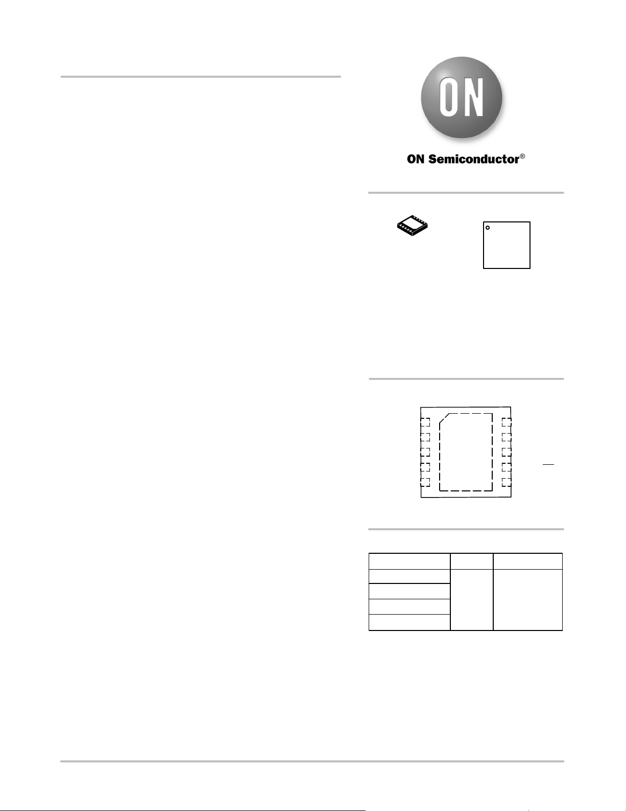
MARKING DIAGRAM
1589x
DFN10
CASE 485C
1589x = Specific Device Code
A = Assembly Location
L = Wafer Lot
Y = Year
W = Work Week
G = Pb−Free Device
(Note: Microdot may be in either location)
BOOT
LX
UG
LG
GND
ORDERING INFORMATION
Device Package Shipping
NCP1589AMNTWG
NCP1589BMNTWG
NCP1589AMNTXG
NCP1589BMNTXG
†For information on tape and reel specifications,
including part orientation and tape sizes, please
refer to our Tape and Reel Packaging Specifications
Brochure, BRD8011/D.
x = A or B
PIN CONNECTIONS
1
2
3
4
5
(Top View)
DFN10
(Pb−Free)
ALYWG
G
PGOOD
10
9 VOS
8
FB
7 COMP/EN
V
6
CC
3000 /
Tape & Reel
†
© Semiconductor Components Industries, LLC, 2009
August, 2009 − Rev. 0
1 Publication Order Number:
NCP1589A/D
NCP1589A, NCP1589B
3.878kW
= 4.5 V − 15 V
V
BST
1mF
VCC
PGOOD
C1
0.0015mF
R4
4.12kW
R1
R2
17.08kW
C2
0.007mF
C3
0.014mF
R3
74.2W
COMP/EN
BOOT
GNDFBVOS
R9 R10
UG
LX
LG
1.02k
0.1mF
ROCSET
1.02k
VIN = 2.5 V − 13.2 VVCC = 4.5 V − 13.2 V
2x0.22mF
VOUT
1.65 V
2x1800mF
GND
2.2
NTD4806 NTD4809
4.7nF
1500mF
1mH
1500mF
3x22mF
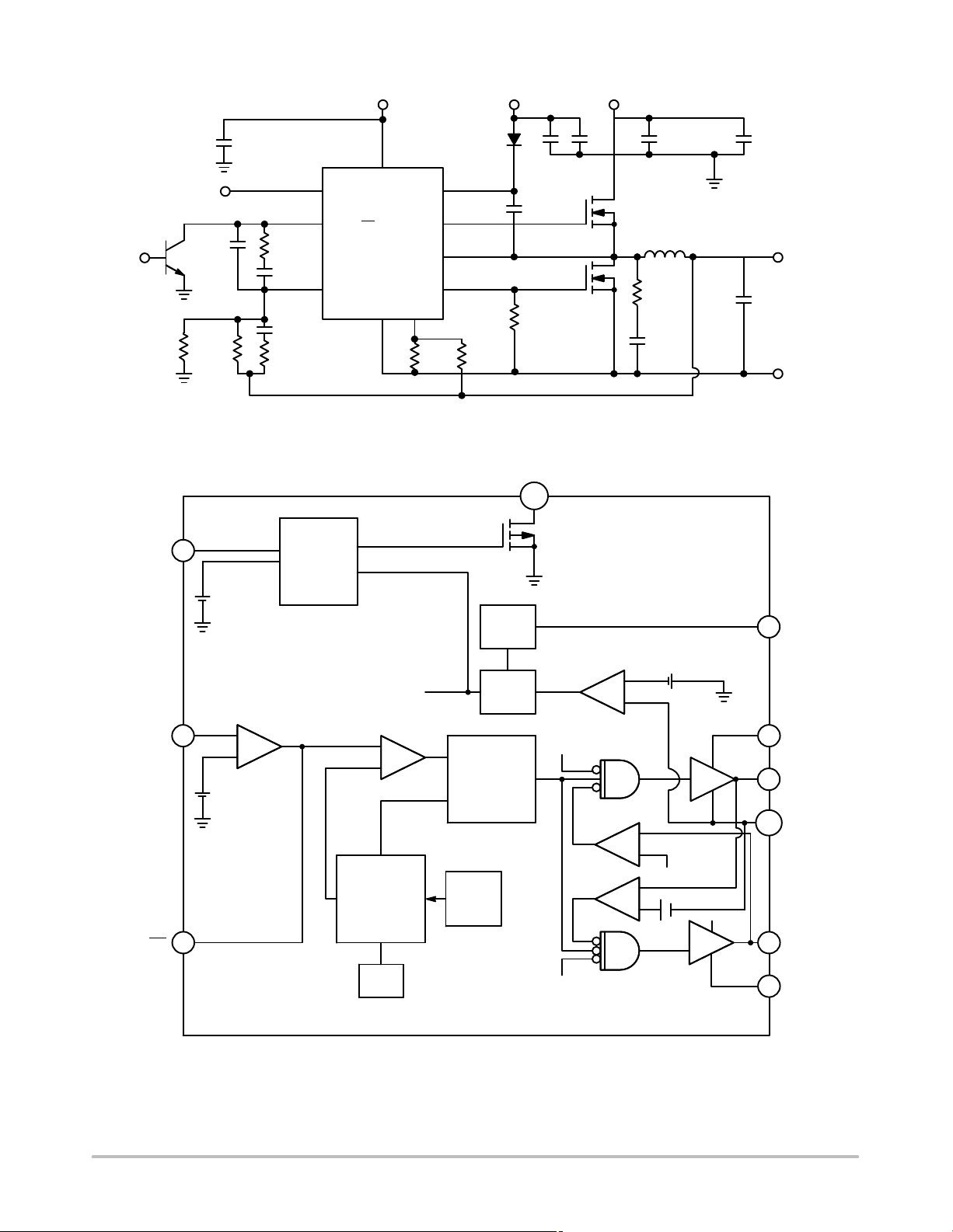
Figure 1. Typical Application Diagram
PGOOD
10
VOS
FB
COMP/EN
9
PGOOD
MONITOR
OV and UV
±10% of V
±25% of V
ref
ref
0.8 V
(V
)
ref
FAULT
8
−
+
+
−
0.8 V
(V
)
ref
CLOCK
RAMP
7
OSC
OSC
R
PWM
OUT
S
SOFT
START
POR
UVLO
LATCH
Q
FAULT
FAULT
VCC
6
+
VOCP
−
1
BOOT
UG
3
LX
+
2
−
2 V
+
−
VCC
LG
4
5
GND
Figure 2. Detailed Block Diagram
http://onsemi.com
2
NCP1589A, NCP1589B
PIN FUNCTION DESCRIPTION
Pin No. Symbol Description
1 BOOT Supply rail for the floating top gate driver. To form a boost circuit, use an external diode to bring the desired
2 LX Switch node pin. This is the reference for the floating top gate driver. Connect this pin to the source of the top
3 UG Top gate MOSFET driver pin. Connect this pin to the gate of the top N−channel MOSFET.
4 LG Bottom gate MOSFET driver pin. Connect this pin to the gate of the bottom N−channel MOSFET.
5 GND IC ground reference. All control circuits are referenced to this pin.
6 VCC
7 COMP/EN Compensation Pin. This is the output of the error amplifier (EA) and the non−inverting input of the PWM com-
8 FB This pin is the inverting input to the error amplifier. Use this pin in conjunction with the COMP pin to com-
9 VOS Voltage Offset Sense
10 PGOOD Power Good output. Pulled Low if VOS is ±10% of 0.8 V V
input voltage to this pin (cathode connected to BOOT pin). Connect a capacitor (C
the LX pin. Typical values for C
range from 0.1 mF to 1 mF. Ensure that C
BOOT
BOOT
) between this pin and
BOOT
is placed near the IC.
MOSFET.
Supply rail for the internal circuitry. Operating supply range is 4.5 V to 13.2 V. Decouple with a 1 mF capacitor
to GND. Ensure that this decoupling capacitor is placed near the IC.
parator. Use this pin in conjunction with the FB pin to compensate the voltage−control feedback loop. Pull this
pin low for disable.
pensate the voltage−control feedback loop. Connect this pin to the output resistor divider (if used) or directly
to V
.
out
.
ref
ABSOLUTE MAXIMUM RATINGS
Pin Name Symbol V
MAX
Main Supply Voltage Input VCC 15 V −0.3 V
Bootstrap Supply Voltage Input BOOT 35 V wrt/GND
40 V < 100 ns
15 V wrt/LX
Switching Node (Bootstrap Supply Return) LX 35 V
40 V for < 100 ns
High−Side Driver Output (Top Gate) UG 30 V wrt/GND
15 V wrt/LX
40 V for < 100 ns
Low−Side Driver Output (Bottom Gate) LG VCC + 0.3 V −0.3 V
Feedback, VOS FB, VOS 5.0 V −0.3 V
COMP/EN COMP/EN 3.6 V −0.3 V
PGOOD PGOOD 7 V −0.3 V
V
MIN
−0.3 V
−0.3 V
−0.3 V
−5 V
−10 V for < 200 ns
−0.3 V wrt/LX
−2 V for < 200 ns
−5 V for < 200 ns
MAXIMUM RATINGS
Rating Symbol Value Unit
Thermal Resistance, Junction−to−Ambient
Thermal Resistance, Junction−to−Case
Operating Junction Temperature Range T
Operating Ambient Temperature Range T
Storage Temperature Range T
R
q
JA
R
q
JC
J
A
stg
Moisture Sensitivity Level MSL 1 −
Stresses exceeding Maximum Ratings may damage the device. Maximum Ratings are stress ratings only. Functional operation above the
Recommended Operating Conditions is not implied. Extended exposure to stresses above the Recommended Operating Conditions may affect
device reliability.
This device is ESD sensitive. Use standard ESD precautions when handling.
165 °C/W
45 °C/W
0 to 150 °C
0 to 70 °C
−55 to +150 °C
http://onsemi.com
3
NCP1589A, NCP1589B
ELECTRICAL CHARACTERISTICS (0°C < T
C
= C
TG
Input Voltage Range 4.5 13.2 V
Boost Voltage Range 13.2 V wrt LX 4.5 30 V
= 1.0 nF, for min/max values unless otherwise noted.)
BG
Characteristic
< 70°C; 4.5 V < [BST−PHASE] < 13.2 V, 4.5 V < BST < 30 V, 0 V < PHASE < 21 V,
A
Conditions Min Typ Max Unit
Supply Current
Quiescent Supply Current (NCP1589A) VFB = 1.0 V, No Switching, VCC = 13.2 V 1.0 8.0 mA
Boost Quiescent Current VFB = 1.0 V, No Switching 0.1
Undervoltage Lockout
UVLO Threshold VCC Rising 3.8 4.0 4.2 V
UVLO Threshold VCC Falling 3.4 3.6 3.8 V
UVLO Hysteresis VCC Rising or VCC Falling 0.4 V
Switching Regulator
VFB Feedback Voltage (FB Tied to Comp. Measure FB Pin.) 0.7936 0.8 0.8064 V
Oscillator Frequency (NCP1589A) 270 300 330 kHz
Oscillator Frequency (NCP1589B) 540 600 660 kHz
Ramp−Amplitude Voltage 1.1 V
Minimum Duty Cycle 0 %
Maximum Duty Cycle 70 75 80 %
LG Minimum on Time 500 ns
Error Amplifier
Open Loop DC Gain (Note 1) 70 80 dB
Output Source Current
Output Sink Current
Input Offset Voltage (Note 1) −2.0 0 2.0 mV
Input Bias Current 0.1 1.0
Unity Gain Bandwidth (Note 1) 15 Mhz
Disable Threshold 0.6 0.8 V
Output Source Current During Disable 10 40
Vfb < 0.8 V
Vfb > 0.8 V
2.0
2.0
Gate Drivers
Upper Gate Source VCC = 5 V, VUG − VLX = 2.5 V 1.5 A
Upper Gate Sink 1.4
Lower Gate Source 1.5 A
Lower Gate Sink VCC = 12 V 1.0
UG Falling to LG Rising Delay VCC = 12 V, UG−LX < 2.0 V, LG > 2.0 V 12.4 18 ns
LG Falling to UG Rising Delay VCC = 12 V, LG < 2.0 V, UG > 2.0 V 12.4 18 ns
Soft−Start
Soft−Start time 3.0 7.0 ms
Power Good
Output Voltage Logic Low, Sinking 4 mA 0.4 V
OVP Threshold to PGOOD Output Low Ramp VOS from 0.7 to 1.2.
Monitor when PGOOD goes Low
OVP Threshold to Part Disable Ramp VOS from 0.8 to 1.2.
Monitor when outputs disable
UVP Threshold to PGOOD Output Low Ramp VOS from 800 mV to 500 mV.
Monitor when PGOOD goes Low
UVP Threshold to Part Disable Ramp VOS from 800 mV to 500 mV.
Monitor when utputs stop switching
0.65 0.72 V
0.5 0.6 V
0.88 1.0 V
1.0 1.2 V
Overcurrent Protection
OC Current Source (Note 1) Sourced from LG pin, before SS 9.0 10 11
1. Guaranteed by design but not tested in production.
mA
mA
mA
mA
W
W
mA
http://onsemi.com
4

NCP1589A, NCP1589B
TYPICAL CHARACTERISTICS
303
VCC = 12 V
302
301
, FREQUENCY (kHz)
300
SW
F
299
010 70
20 30 40 50 60 20 60
, JUNCTION TEMPERATURE (°C)
T
J
VCC = 5 V
Figure 3. Oscillator Frequency (FSW) vs.
Temperature
5.3
5.0
4.7
4.4
(mA)
CC
I
4.1
3.8
NCP1589B
NCP1589A
808
806
804
802
800
798
, REFERENCE (mV)
ref
796
V
794
792
04080
, JUNCTION TEMPERATURE (°C)
T
J
Figure 4. Reference Voltage (V
ref
) vs.
Temperature
543
542
541
540
OCP THRESHOLD (mV)
3.5
020406080
, JUNCTION TEMPERATURE (°C)
T
J
Figure 5. ICC vs. Temperature
539
0 20 406080
, JUNCTION TEMPERATURE (°C)
T
J
Figure 6. OCP Threshold at 55k vs. Temperature
http://onsemi.com
5

NCP1589A, NCP1589B
APPLICATIONS INFORMATION
Over Current Protection (OCP)
The NCP1589A/B monitors the voltage drop across the
low side mosfet and uses this information to determine if
there is excessive output current. The voltage across the low
side mosfet is measured from the LX pin, and is referenced
to ground. The over current measurement is timed to occur
at the end of the low side mosfet conduction period, just
before the bottom mosfet is turned off.
If the voltage drop across the bottom mosfet exceeds the
over current protection threshold, then an internal counter is
incremented. If the voltage drop does not exceed the over
current protection threshold, then the internal counter is
reset. The NCP1589A/B will latch the over current
protection fault condition only if the over current protection
threshold is exceeded for four consecutive cycles.
When the NCP1589A/B latches an over current
protection fault, both the high side and low side mosfets are
turned off. To reset the over current protection fault, the
power to the VCC pin must be cycled.
The over current threshold voltage can be externally, by
varying the value of the ROCSET resistor. The ROCSET
resistor is a resistor connected between the LG pin (low side
mosfet gate) and ground.
During startup, after the VCC and BOOT pins reach the
under voltage lock out threshold, the NCP1589A/B will
source 10 mA of current out of the LG pin. This current will
flow through the ROCSET resistor and produce a voltage
that is sampled and then used as the over current protection
threshold voltage. For example, if ROCSET is set to 10 kW,
the 10 mA of current will yield a 100 mV threshold, and if the
voltage drop across the low side mosfet exceeds 100 mV at
the end of its conduction period, then an over current event
will be detected.
If the ROCSET resistor is not present, then the over
current protection threshold will max out at 640 mV. The
valid range for ROCSET is 5 kW to 55 kW which yields a
threshold voltage range of 50 mV to 550 mV.
Internal Soft-Start
To prevent excess inrush current during startup, the
NCP1589A/B uses a calibrated current source with an
internal soft start capacitor to ramp the reference voltage
from 0 to 800 mV over a period of 4 ms. The softstart ramp
generator will reset if the input power supply voltages reach
the under voltage lockout threshold, or if the NCP1589A/B
is disabled by having the COMP pin pulled low.
Startup into a Precharged Load
During a startup and soft start sequence the NCP1589A
will detect a residual charge on the output capacitors and not
forcefully discharge the capacitors before beginning the
softstart sequence, instead, the softstart ramping of the
output will begin at the voltage level of the residual charge.
For example, if the NCP1589A/B is configured to provide
a regulated output voltage of 2.5 V, the normal softstart
sequence will ramp the output voltage from 0 to 2.5 V in
4.2 ms; however if the output capcitors already have a 1.2 V
charge on them, the NCP1589A/B will not discharge the
capacitors, instead the softstart sequence will begin at 1.2 V
and then ramp the output to 2.5 V.
Power Good
The PGOOD pin is an open drain active high output pin
that signals the condition of the VOS (Voltage Output Sense)
pin. PGOOD is pulled low during soft start cycle, and if there
is a latched over current, over voltage, or under voltage fault.
If the voltage on the VOS pin is within ±10% of Vref
(800 mV) then the PGOOD pin will not be pulled low. The
PGOOD pin does not have an internal pull-up resistor.
Overvoltage Protection
If the voltage on the VOS pin exceeds the over voltage
threshold the NCP1589A/B will latch an over voltage fault.
During an over voltage fault the UG pin will be pulled low,
and the LG pin will be high while the until the voltage on the
VOS pin goes below V
/2 (400 mV). The NCP1589A will
ref
continue drive the LG pin, LG will go high if VOS exceeds
1 V and then go low when VOS goes below 400 mV. The
power to the NCP1589 must be cycled to reset the over
voltage protection fault.
Under Voltage Protection
If the voltage on the VOS pin falls below the under voltage
threshold after the soft start cycle completes, then the
NCP1589A/B will latch an under voltage fault. During an
under voltage fault, both the UG and LG pins will be pulled
low. The power to the NCP1589 must be cycled to reset the
under voltage protection fault.
http://onsemi.com
6

NCP1589A, NCP1589B
V
CC
Internal
UVLO
Fault
COMP
LG
UG
−0.7 V
4.0 V
3.6 V
1.45 V
700 mV
50 mV
OCP
Program-
mable
V
OUT
FB
PGOOD
0.8 V
NORMALSSUVLOPOR
Figure 7. Typical Startup Sequence
http://onsemi.com
7

NCP1589A, NCP1589B
VOS
PGOOD
G
LG
Feedback and Compensation
0.88V
Overvoltage Undervoltage
Figure 8. Typical Power Good Function
0.88V
0.8V
1.0V
0.72V
The NCP1589A/B allows the output voltage to be
adjusted from 0.8 V to 5.0 V via an external resistor divider
network. The controller will try to maintain 0.8 V at
feedback pin. Thus, if a resistor divider circuit was placed
across the feedback pin to V
, the controller will regulate
OUT
the output voltage proportional to the resistor divider
network in order to maintain 0.8 V at the FB pin. The same
formula applies to the VOS pin and the controller will
maintain 0.8 V at the VOS pin.
V
OUT
0.4V
Design Example
Voltage Mode Control Loop with TYPE III
Compensation
Converter Parameters:
Input Voltage: VIN = 5 V
Output Voltage: V
OUT
= 1.65 V
Switching Frequency: 300 kHz
Total Output Capacitance: C
OUT
Total ESR: ESR = 6 mW
Output Inductance: L
Ramp Amplitude: V
OUT
RAMP
: 1 mH
= 1.1 V
0.8V
0.6V
= 3600 mF
R1
FB
R4
Figure 9.
The relationship between the resistor divider network
above and the output voltage is shown in the following
equation:
R4+ R1
ǒ
V
* V
OUT
Ǔ
REF
V
REF
The same formula can be applied to the feedback resistors
at VOS.
V
REF
R9+ R10
ǒ
V
OUT
* V
Ǔ
REF
http://onsemi.com
C1
C3R3
V
OUT
R1
R4
V
ref
Figure 10.
−
+
E/A
a.. Set a target for the close loop bandwidth at 1/6th of
the switching frequency.
F
cross_over
8
:+ 50 kHz
C2R2
V
COMP

NCP1589A, NCP1589B
b.. Output Filter Double Pole Frequency
:+
F
lc
2 @ p @ L
Flc+ 2.653 kHz
1
Ǹ
@ C
OUT
OUT
c.. ESR Zero Frequency:
F
F
ESR
ESR
:+
2 @ p @ C
+ 7.368 kHz
1
OUT
@ C
ESR
Step 1: Set a value for R1 between 2 kW and 5 kW
R1 :+ 4.12 kW
Step 2: Pick compensation DC gain (R2/R1) for desired
close loop bandwidth.
V
:+ 1.1 V
RAMP
V
R2 :+ R1 @
R2 + 17.085 kW
ǒ
RAMP
V
IN
Ǔ@ǒ
F
cross_over
F
lc
Ǔ
Step 3: Place 1st zero at half the output filter double pole
frequency.
Ǹ
2 @ L
C2 :+
C2 + 7.024 10−3mF
OUT
R2
@ C
OUT
Step 4: Place 1st pole at ESR zero frequency.
C1 :+
C2 @ R2 @ 2 @ p @ F
C1 + 1.542 10−3mF
C2
ESR
* 1
Step 5: Place 2nd zero at the output filter double pole
frequency.
F
2@F
SW
R1
* 1
lc
R3 :+
R3 + 74.169 W
Step 6: Place 2nd pole at half the switching frequency.
C3 :+
C3 + 0.014 mF
1
ǒ
p @ R3 @ F
SW
Ǔ
Step 7: R4 is sized to maintain the feedback voltage to
V
= 0.8 V.
ref
V
@ R1
V
REF
OUT
* V
REF
R4 :+
R4 + 3.878 kW
The Component values for Type III Compensation are:
R1 = 4.12 kW
R2 = 17.085 kW
R3 = 74.169 W
R4 = 3.878 kW
C1 = 0.0015 mF
C2 = 0.007 mF
C3 = 0.014 mF
NOTE: Recommend to change values to industry
standard component values.
http://onsemi.com
9

NCP1589A, NCP1589B
PACKAGE DIMENSIONS
DFN10, 3x3, 0.5P
CASE 485C−01
ISSUE B
10X
REFERENCE
2X
2X
10X
10X
PIN 1
0.15 C
0.10 C
0.08 C
L
K
0.15
D
TOP VIEW
C
DETAIL B
(A3)
SIDE VIEW
D2
e
15
A
B
E
A1
DETAIL A
E2
A
C
SEATING
PLANE
EDGE OF PACKAGE
L1
DETAIL A
Bottom View
(Optional)
MOLD CMPD
A1
DETAIL B
Side View
(Optional)
SOLDERING FOOTPRINT*
2.6016
EXPOSED Cu
NOTES:
1. DIMENSIONING AND TOLERANCING PER
ASME Y14.5M, 1994.
2. CONTROLLING DIMENSION: MILLIMETERS.
3. DIMENSION b APPLIES TO PLATED
TERMINAL AND IS MEASURED BETWEEN
0.25 AND 0.30 MM FROM TERMINAL.
4. COPLANARITY APPLIES TO THE EXPOSED
PAD AS WELL AS THE TERMINALS.
5. TERMINAL b MAY HAVE MOLD COMPOUND
MATERIAL ALONG SIDE EDGE. MOLD
FLASHING MAY NOT EXCEED 30 MICRONS
ONTO BOTTOM SURFACE OF TERMINAL b.
6. DETAILS A AND B SHOW OPTIONAL VIEWS
FOR END OF TERMINAL LEAD AT EDGE OF
PACKAGE.
MILLIMETERS
DIM MIN MAX
A3
A 0.80 1.00
A1 0.00 0.05
A3 0.20 REF
b 0.18 0.30
D 3.00 BSC
D2 2.40 2.60
E 3.00 BSC
E2 1.70 1.90
e 0.50 BSC
K 0.19 TYP
L 0.35 0.45
L1 0.00 0.03
3.3048
0.10 C
0.05
C
10X
A B
NOTE 3
b
10 6
BOTTOM VIEW
10X
0.5651
2.1746
0.3008
1.8508
10X
0.5000 PITCH
DIMENSIONS: MILLIMETERS
*For additional information on our Pb−Free strategy and soldering
details, please download the ON Semiconductor Soldering and
Mounting Techniques Reference Manual, SOLDERRM/D.
ON Semiconductor and are registered trademarks of Semiconductor Components Industries, LLC (SCILLC). SCILLC reserves the right to make changes without further notice
to any products herein. SCILLC makes no warranty, representation or guarantee regarding the suitability of its products for any particular purpose, nor does SCILLC assume any liability
arising out of the application or use of any product or circuit, and specifically disclaims any and all liability, including without limitation special, consequential or incidental damages.
“Typical” parameters which may be provided in SCILLC data sheets and/or specifications can and do vary in different applications and actual performance may vary over time. All
operating parameters, including “Typicals” must be validated for each customer application by customer’s technical experts. SCILLC does not convey any license under its patent rights
nor the rights of others. SCILLC products are not designed, intended, or authorized for use as components in systems intended for surgical implant into the body, or other applications
intended to support or sustain life, or for any other application in which the failure of the SCILLC product could create a situation where personal injury or death may occur. Should
Buyer purchase or use SCILLC products for any such unintended or unauthorized application, Buyer shall indemnify and hold SCILLC and its officers, employees, subsidiaries, affiliates,
and distributors harmless against all claims, costs, damages, and expenses, and reasonable attorney fees arising out of, directly or indirectly, any claim of personal injury or death
associated with such unintended or unauthorized use, even if such claim alleges that SCILLC was negligent regarding the design or manufacture of the part. SCILLC is an Equal
Opportunity/Affirmative Action Employer. This literature is subject to all applicable copyright laws and is not for resale in any manner.
PUBLICATION ORDERING INFORMATION
LITERATURE FULFILLMENT:
Literature Distribution Center for ON Semiconductor
P.O. Box 5163, Denver, Colorado 80217 USA
Phone: 303−675−2175 or 800−344−3860 Toll Free USA/Canada
Fax: 303−675−2176 or 800−344−3867 Toll Free USA/Canada
Email: orderlit@onsemi.com
N. American Technical Support: 800−282−9855 Toll Free
USA/Canada
Europe, Middle East and Africa Technical Support:
Phone: 421 33 790 2910
Japan Customer Focus Center
Phone: 81−3−5773−3850
http://onsemi.com
ON Semiconductor Website: www.onsemi.com
Order Literature: http://www.onsemi.com/orderlit
For additional information, please contact your local
Sales Representative
NCP1589A/D
10

 Loading...