ON NCP1402SN19T1, NCP1402SN27T1, NCP1402SN30T1, NCP1402SN33T1, NCP1402SN40T1 Schematic [ru]
...
NCP1402
200 mA, PFM Step−Up
Micropower Switching
Regulator
The NCP1402 series are monolithic micropower step−up DC to DC
converter that are specially designed for powering portable equipment
from one or two cell battery packs.These devices are designed to
startup with a cell voltage of 0.8 V and operate down to less than
0.3 V. With only three external components, this series allow a simple
means to implement highly efficient converters that are capable of up
to 200 mA of output current at V
Each device consists of an on−chip PFM (Pulse Frequency
Modulation) oscillator, PFM controller, PFM comparator, soft−start,
voltage reference, feedback resistors, driver, and power MOSFET
switch with current limit protection. Additionally, a chip enable
feature is provided to power down the converter for extended battery
life.
The NCP1402 device series are available in the Thin SOT−23−5
package with five standard regulated output voltages. Additional
voltages that range from 1.8 V to 5.0 V in 100 mV steps can be
manufactured.
Features
• Pb−Free Packages are Available
• Extremely Low Startup Voltage of 0.8 V
• Operation Down to Less than 0.3 V
• High Efficiency 85% (V
• Low Operating Current of 30 A (V
• Output Voltage Accuracy ± 2.5%
• Low Converter Ripple with Typical 30 mV
• Only Three External Components Are Required
• Chip Enable Power Down Capability for Extended Battery Life
• Micro Miniature Thin SOT−23−5 Packages
in
= 2.0 V, V
in
= 2.0 V, V
OUT
= 1.9 V)
OUT
= 3.0 V.
OUT
= 3.0 V, 70 mA)
http://onsemi.com
5
1
SOT23−5
(TSOP−5, SC59−5)
SN SUFFIX
CASE 483
PIN CONNECTIONS AND
MARKING DIAGRAM
1
CE
2
OUT
3
NC
xxx = Marking
Y = Year
W = Work Week
(Top View)
ORDERING INFORMATION
See detailed ordering and shipping information in the ordering
information section on page 3 of this data sheet.
xxxYW
5
LX
GND
4
T ypical Applications
• Cellular Telephones
• Pagers
• Personal Digital Assistants (PDA)
• Electronic Games
• Portable Audio (MP3)
• Camcorders
• Digital Cameras
• Handheld Instruments
Semiconductor Components Industries, LLC, 2004
October, 2004 − Rev. 6
1 Publication Order Number:
NCP1402/D

NCP1402
1
CE
Chi Enable in
() g q g
OUT
NC
GND
V
in
CE
OUT
NC
1
NCP1402
2
3
LX
5
GND
4
V
OUT
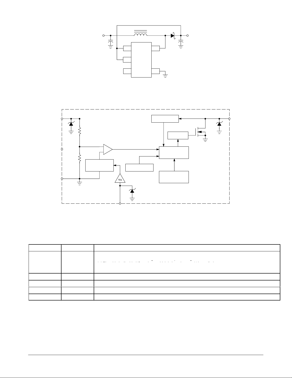
Figure 1. T ypical Step−Up Converter Application
2
PFM
COMPARATOR
−
3
REFERENCE
4
+
VOLTAGE
SOFT−START
VLX LIMITER
DRIVER
POWER
SWITCH
PFM
CONTROLLER
PFM
OSCILLATOR
LX
5
1 CE
Figure 2. Representative Block Diagram
PIN FUNCTION DESCRIPTIONS
Pin # Symbol Pin Description
1 CE Chip Enable pin
2 OUT Output voltage monitor pin, also the power supply pin of the device
3 NC No internal connection to this pin
4 GND Ground pin
5 LX External inductor connection pin to power switch drain
(1) The chip is enabled if a voltage which is equal to or greater than 0.9 V is applied
(2) The chip is disabled if a voltage which is less than 0.3 V is applied
(3) The chip will be enabled if it is left floating
http://onsemi.com
2

NCP1402
Á
Á
Á
Á
Á
Á
Á
Á
Á
Á
Á
Á
ORDERING INFORMATION
Device Output Voltage Device Marking Package Shipping
NCP1402SN19T1 1.9 V DAU
NCP1402SN27T1 2.7 V DAE
NCP1402SN30T1 3.0 V DAF
SOT23−5
NCP1402SN33T1 3.3 V DAG
NCP1402SN33T1G 3.3 V DAG SOT23−5
(Pb−Free)
3000 Units Per Reel
NCP1402SN40T1 4.0 V DCR
NCP1402SN50T1 5.0 V DAH
NCP1402SN50T1G 5.0 V DAH
SOT23−5
SOT23−5
(Pb−Free)
†For information on tape and reel specifications, including part orientation and tape sizes, please refer to our Tape and Reel Packaging
Specifications Brochure, BRD8011/D.
NOTE: The ordering information lists five standard output voltage device options. Additional device with output voltage ranging from 1.8 V to
5.0 V in 100 mV increments can be manufactured. Contact your ON Semiconductor representative for availability.
ABSOLUTE MAXIMUM RATINGS
Rating Symbol Value Unit
Power Supply Voltage (Pin 2)
Input/Output Pins
БББББББББББББББББББББ
LX (Pin 5)
LX Peak Sink Current
БББББББББББББББББББББ
CE (Pin 1)
Input Voltage Range
БББББББББББББББББББББ
Input Current Range
Thermal Resistance, Junction−to−Air
Operating Ambient Temperature Range (Note 2)
Operating Junction Temperature Range
Storage Temperature Range
Maximum ratings are those values beyond which device damage can occur. Maximum ratings applied to the device are individual stress limit
values (not normal operating conditions) and are not valid simultaneously . If these limits are exceeded, device functional operation is not implied,
damage may occur and reliability may be affected.
NOTES:
1. This device series contains ESD protection and exceeds the following tests:
Human Body Model (HBM) ±2.0 kV per JEDEC standard: JESD22−A114.
Machine Model (MM) ±200 V per JEDEC standard: JESD22−A115.
2. The maximum package power dissipation limit must not be exceeded.
T
P
D
J(max)
R
JA
T
A
3. Latchup Current Maximum Rating: ±150 mA per JEDEC standard: JESD78.
4. Moisture Sensitivity Level: MSL 1 per IPC/JEDEC standard: J−STD−020A.
V
OUT
ÁÁ
V
LX
I
LX
ÁÁ
V
CE
ÁÁ
I
CE
R
JA
T
A
T
J
T
stg
6.0
ÁÁÁÁ
−0.3 to 6.0
400
ÁÁÁÁ
−0.3 to 6.0
ÁÁÁÁ
−150 to 150
250
−40 to +85
−40 to +125
−55 to +150
†
Á
mA
Á
Á
mA
°C/W
°C
°C
°C
V
V
V
http://onsemi.com
3

NCP1402
ELECTRICAL CHARACTERISTICS (For all values T
= 25°C, unless otherwise noted.)
A
Characteristic
OSCILLATOR
Switch On Time (current limit not asserted)
Switch Minimum Off Time t
Maximum Duty Cycle D
Minimum Startup Voltage (IO = 0 mA) V
Minimum Startup Voltage Temperature Coefficient (TA = −40°C to 85°C) V
Minimum Operation Hold Voltage (IO = 0 mA) V
Soft−Start Time (V
0.8 V) t
OUT
LX (PIN 5)
Internal Switching N−Channel FET Drain Voltage
LX Pin On−State Sink Current (VLX = 0.4 V)
Device Suffix:
19T1
27T1
30T1
33T1
40T1
50T1
Voltage Limit V
Off−State Leakage Current (VLX = 6.0 V, TA = −40°C to 85°C) I
CE (PIN 1)
CE Input Voltage (V
OUT
= V
SET
x 0.96)
High State, Device Enabled
Low State, Device Disabled
CE Input Current (Note 6)
High State, Device Enabled (V
Low State, Device Disabled (V
= VCE = 6.0 V)
OUT
= 6.0 V, VCE = 0 V)
OUT
TOTAL DEVICE
Output Voltage
Device Suffix:
19T1
27T1
30T1
33T1
40T1
50T1
Output Voltage Temperature Coefficient (TA = −40°C to +85°C)
Device Suffix:
19T1
27T1
30T1
33T1
40T1
50T1
Operating Current 2 (V
Off−State Current (V
Operating Current 1 (V
= VCE = V
OUT
= 5.0 V, VCE = 0 V, TA = −40°C to +85°C, Note 6) I
OUT
= VCE = V
OUT
+0.5 V, Note 5) I
SET
x 0.96)
SET
Device Suffix:
19T1
27T1
30T1
33T1
40T1
50T1
5. V
means setting of output voltage.
SET
6. CE pin is integrated with an internal 10 M pullup resistor.
Symbol Min Typ Max Unit
t
on
off
MAX
start
start
hold
SS
V
LX
I
LX
LXLIM
LKG
3.6 5.5 7.6 s
1.0 1.45 1.9 s
70 78 85 %
− 0.8 0.95 V
− −1.6 − mV/°C
0.3 − − V
0.3 2.0 − ms
− − 6.0 V
mA
110
130
130
130
130
130
145
180
190
200
210
215
−
−
−
−
−
−
0.45 0.65 0.9 V
− 0.5 1.0 A
V
V
CE(high)
V
CE(low)
0.9
−
−
−
−
0.3
A
I
CE(high)
I
CE(low)
V
OUT
V
OUT
DD2
OFF
I
DD1
−0.5
−0.5
1.853
2.632
2.925
3.218
3.900
4.875
−
−
−
−
−
−
0
0.15
1.9
2.7
3.0
3.3
4.0
5.0
150
150
150
150
150
150
0.5
0.5
1.948
2.768
3.075
3.383
4.100
5.125
−
−
−
−
−
−
− 13 15 A
− 0.6 1.0 A
−
−
−
−
−
−
30
39
42
45
55
70
50
60
60
60
100
100
V
ppm/°C
A
http://onsemi.com
4

NCP1402
2.1
2.0
1.9
1.8
, OUTPUT VOLTAGE (V)
1.7
OUT
V
1.6
0
Vin = 0.9 V
I
O
Vin = 1.2 V
604020
80 100 120 140 160 180 200 0 604020 80 100 120 140 160 180 200
, OUTPUT CURRENT (mA)
NCP1402SN19T1
L = 47 H
= 25°C
T
A
Vin = 1.5 V
Figure 3. NCP1402SN19T1 Output Voltage vs.
Output Current
6.0
Vin = 4.0 V
5.0
4.0
3.0
, OUTPUT VOLTAGE (V)
2.0
OUT
V
1.0
Vin = 1.2 V
Vin = 0.9 V
NCP1402SN50T1
L = 47 H
T
= 25°C
A
0604020 80 100 120 140 160 180 200 0 604020 80 100 120 140 160 180 200
IO, OUTPUT CURRENT (mA)
Vin = 1.5 V
Vin = 2.0 V
Vin = 3.0 V
4.0
NCP1402SN30T1
L = 47 H
3.5
3.0
2.5
, OUTPUT VOLTAGE (V)
2.0
OUT
V
1.5
= 25°C
T
A
Vin = 0.9 V
Vin = 1.5 V
Vin = 1.2 V
I
, OUTPUT CURRENT (mA)
O
Figure 4. NCP1402SN30T1 Output Voltage vs.
Output Current
100
80
60
40
EFFICIENCY (%)
20
Vin = 0.9 V Vin = 1.2 V
NCP1402SN19T1
L = 47 H
T
= 25°C
A
0
IO, OUTPUT CURRENT (mA)
Vin = 1.5 V
Vin = 2.5 V
Vin = 2.0 V
Figure 5. NCP1402SN50T1 Output Voltage vs.
Output Current
100
Vin = 2.5 V
80
Vin = 2.0 V
60
Vin = 0.9 V Vin = 1.2 V Vin = 1.5 V
40
EFFICIENCY (%)
NCP1402SN30T1
20
L = 47 H
= 25°C
T
A
0
0604020 80 100 120 140 160 180 200
IO, OUTPUT CURRENT (mA)
Figure 7. NCP1402SN30T1 Efficiency vs.
Output Current
100
80
60
40
EFFICIENCY (%)
20
0
http://onsemi.com
5
Figure 6. NCP1402SN19T1 Efficiency vs.
Output Current
Vin = 4.0 V
Vin = 3.0 V
Vin = 1.2 V
Vin = 0.9 V
NCP1402SN50T1
L = 47 H
= 25°C
T
A
0604020 80 100 120 140 160 180 200
IO, OUTPUT CURRENT (mA)
Vin = 1.5 V
Vin = 2.0 V
Figure 8. NCP1402SN50T1 Efficiency vs.
Output Current

NCP1402
0
0
2.1
2.0
1.9
1.8
, OUTPUT VOLTAGE (V)
1.7
NCP1402SN19T1
OUT
V
V
= 1.9 V x 0.96
OUT
Open−Loop Test
1.6
−50
250−25
50 75 100 −50 250−25 50 75 10
TEMPERATURE (°C)
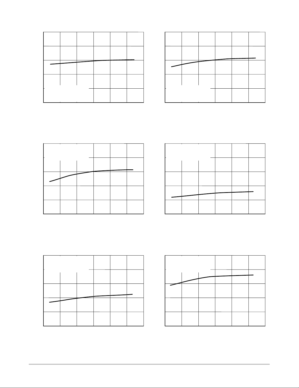
Figure 9. NCP1402SN19T1 Output Voltage vs.
Temperature
5.2
NCP1402SN50T1
V
= 5.0 V x 0.96
OUT
Open−Loop Test
5.1
5.0
3.2
3.1
3.0
2.9
, OUTPUT VOLTAGE (V)
2.8
NCP1402SN30T1
OUT
V
V
= 3.0 V x 0.96
OUT
Open−Loop Test
2.7
TEMPERATURE (°C)
Figure 10. NCP1402SN30T1 Output Voltage vs.
Temperature
100
NCP1402SN19T1
V
= 1.9 V x 0.96
OUT
Open−Loop Test
80
60
4.9
40
, OUTPUT VOLTAGE (V)
4.8
OUT
V
4.7
−50 250−25 50 75 100 −50 250−25 50 75 10
TEMPERATURE (°C)
Figure 11. NCP1402SN50T1 Output Voltage vs.
Temperature
20
, OPERATING CURRENT 1 (mA)
DD1
I
0
Figure 12. NCP1402SN19T1 Operating
Current 1 vs. Temperature
TEMPERATURE (°C)
100
NCP1402SN30T1
V
= 3.0 V x 0.96
OUT
Open−Loop Test
80
60
40
20
, OPERATING CURRENT 1 (mA)
DD1
I
0
100
NCP1402SN50T1
V
= 5.0 V x 0.96
OUT
Open−Loop Test
80
60
40
20
, OPERATING CURRENT 1 (mA)
DD1
I
0
−50 250−25 50 75 100 −50 250−25 50 75 100
TEMPERATURE (°C)
TEMPERATURE (°C)
Figure 13. NCP1402SN30T1 Operating
Current 1 vs. Temperature
Figure 14. NCP1402SN50T1 Operating
Current 1 vs. Temperature
http://onsemi.com
6
 Loading...