

Page 1
NCP1392B
High-Voltage Half-Bridge
Driver with Inbuilt
Oscillator
The NCP1392B is a self−oscillating high voltage MOSFET driver
primarily tailored for the applications using half bridge topology. Due
to its proprietary high−voltage technology, the driver accepts bulk
voltages up to 600 V. Operating frequency of the driver can be
adjusted from 25 kHz to 250 kHz using a single resistor. Adjustable
Brown−out protection assures correct bulk voltage operating range.
An internal 100 ms PFC delay timer guarantee that the main
downstream converter will be turned on in the time the bulk voltage is
fully stabilized. The device provides fixed dead time which helps
lowering the shoot−through current.
Features
• Wide Operating Frequency Range − from 25 kHz to 250 kHz
• Minimum frequency adjust accuracy $3%
• Fixed Dead Time − 0.6 ms
• Adjustable Brown−out Protection for a Simple PFC Association
• 100 ms PFC Delay Timer
• Non−latched Enable Input
• Internal 16 V V
• Low Startup Current of 50 mA
• 1 A / 0.5 A Peak Current Sink / Source Drive Capability
• Operation up to 600 V Bulk Voltage
• Internal Temperature Shutdown
• SOIC−8 or PDIP−8 Package
• These are Pb−Free Devices
CC
Clamp
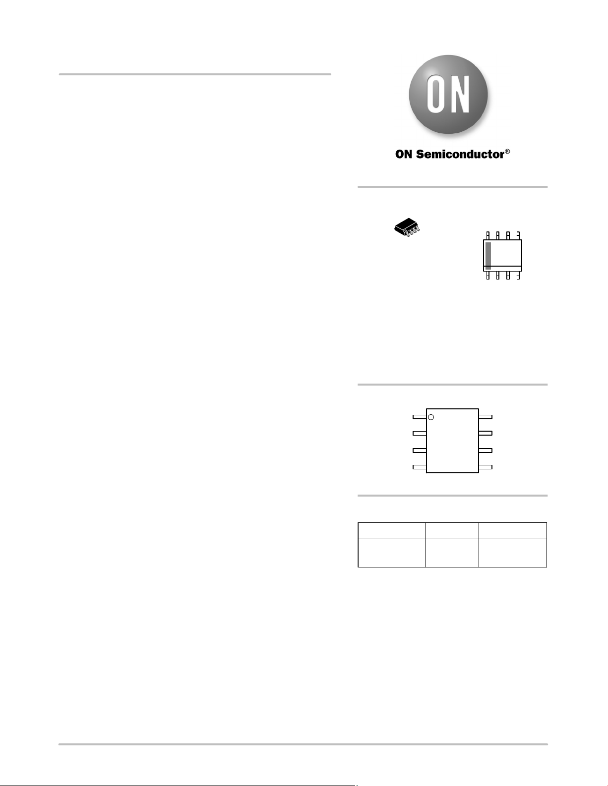
http://onsemi.com
DIAGRAMS
8
1
SOIC−8
CASE 751
A = Assembly Location
L = Wafer Lot
Y = Year
WW = Work Week
G = Pb−Free Package
PINOUT
VCC
Rt
BO
GND
8
1
MARKING
1392B
ALYWW
G
Vboot
Mupper
HB
Mlower
Typical Applications
• Flat Panel Display Power Converters
• Low Cost Resonant SMPS
• High Power AC/DC Adapters for Notebooks
• Offline Battery Chargers
• Lamp Ballasts
© Semiconductor Components Industries, LLC, 2008
October, 2008 − Rev. 1
ORDERING INFORMATION
Device Package Shipping
NCP1392BDR2G SOIC−8
†For information on tape and reel specifications,
including part orientation and tape sizes, please
refer to our Tape and Reel Packaging Specifications
Brochure, BRD8011/D.
1 Publication Order Number:
(Pb−Free)
Tape & Reel
†
2500 /
NCP1392/D
Page 2
NCP1392B
AC
OUTPUT
PFC FRONT STAGE
+
Cbulk
Rbo2
Rbo1
Dboot
VCC
Vboot
Rt
Mupper
Bo
GND
Mlower
NCP1392
Rf
Rfmax
Rfstart
CSS
Cboot
HB
M1
M2
Figure 1. Typical Application Example
PIN FUNCTION DESCRIPTION
Pin # Pin Name Function Pin Description
1 V
CC
2 Rt Timing Resistor Connecting a resistor between this pin and GND, sets the operating frequency
3 BO Brown−Out Detects low input voltage conditions. When brought above Vref_EN, it stops the
4 GND IC Ground
5 Mlower Low−Side Driver Output Drives the lower side MOSFET
6 HB Half−Bridge Connection Connects to the half−bridge output
7 Mupper High−Side Driver Output Drives the higher side MOSFET
8 Vboot Bootstrap Pin The floating supply terminal for the upper stage
Supplies the Driver The driver accepts up to 16 V (given by internal zener clamp)
driver. Operation is restored (without any delay) when BO pin voltage drops
100 mV below Vref_EN.
+
DC
OUTPUT
http://onsemi.com
2
Page 3
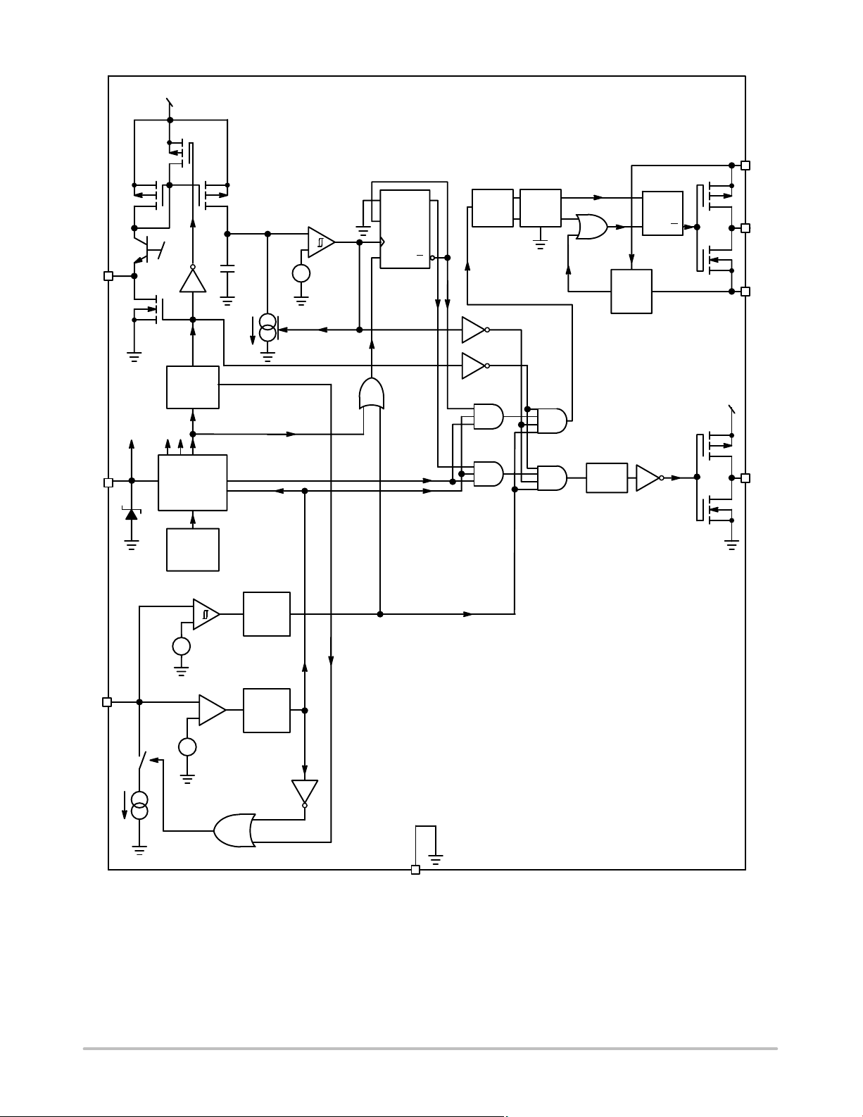
NCP1392B
V
DD
V
boot
UV
Detect
SRQ
M
Q
upper
Bridge
V
CC
M
lower
S
Q
+
V
V
DD
V
CC
Clamp
ref
PFC Delay
(100ms)
V
ref
PON
RESET
V
CC
Management
TSD
−
+
+
Vref
−
C
t
I
DT
0.5ms
Filter
EN
Rt
V
CC
V
CC
−
+
V
ref
−
D
CLK
R
Q
Pulse
Trigger
Level
Shifter
DELAY
BO
SW
hyster
I
+
−
+
Vref
−
20ms
Filter
BO
HIGH Level for 50ms After V
On
CC
GND
Figure 2. Internal Circuit Architecture
http://onsemi.com
3
Page 4
NCP1392B
MAXIMUM RATINGS TABLE
Symbol Rating Value Unit
Vbridge High Voltage Bridge Pin − Pin 6 −1 to +600 V
Vboot −
Vbridge
VDRV_HI High−Side Output Voltage Vbridge − 0.3 to
VDRV_LO Low−Side Output Voltage −0.3 to VCC +0.3 V
dVbridge/dt Allowable Output Slew Rate $50 V/ns
I
CC
V_Rt Rt Pin Voltage −0.3 to 5 V
R
q
R
q
Stresses exceeding Maximum Ratings may damage the device. Maximum Ratings are stress ratings only. Functional operation above the
Recommended Operating Conditions is not implied. Extended exposure to stresses above the Recommended Operating Conditions may affect
device reliability.
1. This device contains internal zener clamp connected between V
by an external resistor when device is supplied from supply which voltage is higher than VCC
specified for VBO = 0 V.
Floating Supply Voltage 0 to 20 V
Vboot + 0.3
Maximum Current that Can Flow into VCC Pin (Pin 1), (Note 1) 20 mA
Maximum Voltage, All Pins (Except Pins 4 and 5) −0.3 to 10 V
Thermal Resistance Junction−to−Air, IC Soldered on 50 mm2 Cooper 35 mm
JA
Thermal Resistance Junction−to−Air, IC Soldered on 200 mm2 Cooper 35 mm
JA
178 °C/W
147 °C/W
Storage Temperature Range −60 to +150 °C
ESD Capability, Human Body Model (All Pins Except Pins 1 , 6, 7 and 8) 2 kV
ESD Capability, Machine Model (All Pins Except Pins 1, 6, 7 and 8) 200 V
and GND terminals. Current flowing into the VCC pin has to be limited
CC
(16 V typically). The ICC parameter is
clamp
V
http://onsemi.com
4
Page 5
NCP1392B
ELECTRICAL CHARACTERISTICS (For typical values T
V
= 12 V, unless otherwise noted)
CC
Characteristic
= 25°C, for min/max values TJ = −40°C to +125°C, Max TJ = 150°C,
J
Pin Symbol Min Typ Max Unit
SUPPLY SECTION
Turn−On Threshold Level, V
Going Up 1 VCC
CC
Minimum Operating Voltage after Turn−On 1 VCC
Startup Voltage on the Floating Section 1 Vboot
Cutoff Voltage on the Floating Section, 1 Vboot
VCC Level at which the Internal Logic gets Reset 1 VCC
Startup Current, VCC < VCCON, 0°C v T
Startup Current, VCC < VCCON, −40°C v T
v +125°C 1 I
amb
< 0°C 1 I
amb
ON
min
ON
min
reset
CC
CC
10 11 12 V
8 9 10 V
7.8 8.8 9.8 V
7 8 9 V
− 6.5 − V
− − 50
− − 65
mA
mA
Internal IC Consumption, No Output Load on Pins 8/7 − 5/4, Fsw = 100 kHz 1 ICC1 − 2.2 − mA
Internal IC Consumption, 1 nF Output Load on Pins 8/7 − 5/4, Fsw = 100 kHz 1 ICC2 − 3.4 − mA
Consumption in Fault Mode (Drivers Disabled, VCC > V
Consumption During PFC Delay Period, 0°C v T
Consumption During PFC Delay Period, −40°C v T
amb
amb
v +125°C ICC4 − − 400
, RT = 3.5 kW)
CC(min)
< 0°C ICC4 − − 470
Internal IC Consumption, No Output Load on Pin 8/7 FSW = 100 kHz 8 I
Internal IC Consumption, 1 nF Load on Pin 8/7 FSW = 100 kHz 8 I
Consumption in Fault Mode (Drivers Disabled, V
boot
> Vboot
) 8 I
min
VCC Zener Clamp Voltage @ 20 mA 1 VCC
1 ICC3 − 2.56 − mA
mA
mA
boot1
boot2
boot3
clamp
− 0.3 − mA
− 1.44 − mA
− 0.1 − mA
15.4 16 17.5 V
INTERNAL OSCILLATOR
Minimum Switching Frequency,
= 35 kW on Pin 2, DT = 600 ns
R
t
Maximum Switching Frequency, Rt = 3.5 kW on Pin 2, DT = 600 ns
Reference Voltage for all Current Generations 2 V
Internal Resistance Discharging C
soft−start
2 FSW min 24.25 25 25.75 kHz
2 FSW max 208 245 282 kHz
RT 3.33 3.5 3.67 V
ref
2 Rt
discharge
− 500 −
W
Operating Duty Cycle Symmetry 5, 7 DC 48 50 52 %
NOTE: Maximum capacitance directly connected to Pin 2 must be under 100 pF.
DRIVE OUTPUT
Output Voltage Rise Time @ CL = 1 nF, 10−90% of Output Signal
5, 7 T
Output Voltage Fall Time @ CL = 1 nF, 10−90% of Output Signal 5, 7 T
Source Resistance 5, 7 R
Sink Resistance 5, 7 R
Deadtime 5,7 T
Leakage Current on High Voltage Pins to GND (600 Vdc) 6,7,8 IHV
r
f
OH
OL
dead
Leak
− 40 − ns
− 20 − ns
− 12 −
− 5 −
540 610 720 ns
− − 5
mA
W
W
PROTECTION
Brown−Out Input Bias Current
3 IBO
bias
− 0.01 −
mA
Brown−Out Level 3 VBO 0.95 1 1.05 V
Hysteresis Current, V
Reference Voltage for EN Input 3 V
< VBO 3 IBO 15.6 18.2 20.7
pin3
EN 1.9 2 2.1 V
ref
mA
Enable Comparator Hysteresis 3 EN_Hyste − 100 − mV
Propagation Delay Before Drivers are Stopped 3 EN_Delay − 0.5 −
ms
Delay Before Any Driver Restart − PFC Delay − 100 − ms
Temperature Shutdown − TSD 140 − − °C
Hysteresis − TSDhyste − 30 − °C
http://onsemi.com
5
Page 6
NCP1392B
11.01
11.00
10.99
10.98
10.97
10.96
10.95
VOLTAGE (V)
10.94
10.93
10.92
10.91
−40 −20 0 20 40 60 80 100 120
TEMPERATURE (°C)
8.85
8.80
8.75
8.70
VOLTAGE (V)
8.65
8.60
Figure 3. V
CCon
8.98
8.97
8.96
8.95
8.94
VOLTAGE (V)
8.93
8.92
8.91
8.90
−40 −20 0 20 40 60 80 100 120
TEMPERATURE (°C)
8.10
8.05
8.00
7.95
7.90
VOLTAGE (V)
7.85
7.80
Figure 4. V
CCmin
8.55
−40 −20 0 20 40 60 80 100 120
TEMPERATURE (°C)
Figure 5. V
20
18
16
14
12
10
8
6
RESISTANCE (W)
4
2
0
−40 −20 0 20 40 60 80 100 120
TEMPERATURE (°C)
Figure 7. R
BOOTon
OH
7.75
−40 −20 0 20 40 60 80 100 120
TEMPERATURE (°C)
Figure 6. V
8
7
6
5
4
3
RESISTANCE (W)
2
1
0
−40 −20 0 20 40 60 80 100 120
TEMPERATURE (°C)
Figure 8. R
BOOTmin
OL
http://onsemi.com
6
Page 7

NCP1392B
243.4
243.2
243.0
242.8
242.6
242.4
FREQUENCY (kHz)
242.2
242.0
241.8
−40 −20 0 20 40 60 80 100 120
TEMPERATURE (°C)
Figure 9. F
45.0
40.0
35.0
30.0
25.0
20.0
15.0
CURRENT (mA)
10.0
5.0
0.0
−40 −20 0 20 40 60 80 100 120
TEMPERATURE (°C)
Figure 11. I
SWmax
CC_startup
25.05
25.00
24.95
24.90
24.85
FREQUENCY (kHz)
24.80
24.75
−40 −20 0 20 40 60 80 100 120
TEMPERATURE (°C)
Figure 10. F
450
400
350
300
250
200
150
CURRENT (mA)
100
50
0
−40 −20 0 20 40 60 80 100 120
TEMPERATURE (°C)
Figure 12. I
SWmin
CC4
580
560
540
520
500
480
460
RESISTANCE (W)
440
420
400
−40 −20 0 20 40 60 80 100 120
TEMPERATURE (°C)
Figure 13. Rt_
discharge
645
640
635
630
625
TIME (ns)
620
615
610
http://onsemi.com
7
−40 −20 0 20 40 60 80 100 120
TEMPERATURE (°C)
Figure 14. T
dead
Page 8

NCP1392B
109
108
107
106
105
104
TIME (ms)
103
102
101
100
90
−40 −20 0 20 40 60 80 100 120
TEMPERATURE (°C)
Figure 15. PFC
1.015
1.014
1.013
1.012
1.011
1.010
VOLTAGE (V)
1.009
1.008
1.007
−40 −20 0 20 40 60 80 100 120
TEMPERATURE (°C)
Figure 17. V
delay
BO
2.008
2.006
2.004
2.002
2.000
1.998
VOLTAGE (V)
1.996
1.994
1.992
1.990
−40 −20 0 20 40 60 80 100 120
TEMPERATURE (°C)
Figure 16. V
110
108
106
104
102
100
98
VOLTAGE (mV)
96
94
92
90
−40 −20 0 20 40 60 80 100 120
TEMPERATURE (°C)
Figure 18. EN
ref_EN
hyste
19.4
19.2
19.0
18.8
18.6
18.4
18.2
CURRENT (mA)
18.0
17.8
17.6
17.4
−40 −20 0 20 40 60 80 100 120
TEMPERATURE (°C)
Figure 19. I
BO
17.0
16.8
16.6
16.4
VOLTAGE (V)
16.2
16.0
15.8
http://onsemi.com
8
−40 −20 0 20 40 60 80 100 120
TEMPERATURE (°C)
Figure 20. V
CC_clamp
Page 9

290
240
190
140
FREQUENCY (kHz)
90
40
0.3 0.4 0.5 0.6 0.7 0.8 0.9 1.0 1.1 1.2
0.2
Figure 21. Irt and Appropriate Frequency
NCP1392B
Irt (mA)
APPLICATION INFORMATION
The NCP1392 is primarily intended to drive low cost half
bridge applications and especially resonant half bridge
applications. The IC includes several features that help the
designer to cope with resonant SPMS design. All features
are described thereafter:
• Wide Operating Frequency Range: The internal
current controlled oscillator is capable to operate over
wide frequency range up to 250 kHz. Minimum
frequency accuracy is $3%.
• Fixed Dead−Time: The internal dead−time helping to
fight with cross conduction between the upper and
lower power transistors. Three versions with different
dead time values are available to cover wide range of
applications.
• 100 ms PFC Timer: Fixed delay is placed to IC
operation whenever the driver restarts (VCC
BO_OK detect events). This delay assures that the bulk
voltage will be stabilized in the time the driver provides
pulses on the outputs. Another benefit of this delay is
that the soft start capacitor will be full discharged
before any restart.
ON
or
• Brown−Out Detection: The BO input monitors bulk
voltage level via resistor divider and thus assures that
the application is working only for wanted bulk voltage
band. The BO input sinks current of 18.2 mA until the
threshold is reached. Designer can thus adjust
Vref
BO
the bulk voltage hysteresis according to the application
needs.
• Non−Latched Enable Input: The enable comparator
input is connected in parallel to the BO terminal to
allow the designer stop the output drivers when needed.
There is no PFC delay when enable input is released so
skip mode for resonant SMPS applications and
dimming for light ballast applications are possible.
• Internal V
Clamp: The internal zener clamp offers
CC
a way to prepare passive voltage regulator to maintain
voltage at 16 V in case the controller is supplied
V
CC
from unregulated power supply or from bulk capacitor.
• Low Startup Current: This device features maximum
startup current of 50 mA which allows the designer to
use high value startup resistor for applications when
driver is supplied from the auxiliary winding. Power
dissipation of startup resistor is thus significantly
reduced.
Current Controlled Oscillator
The current controlled oscillator features a high−speed
circuitry allowing operation from 50 kHz up to 500 kHz.
However, as a division by two internally creates the two Q
and Q
outputs, the final effective signal on output Mlower
and Mupper switches between 25 kHz and 250 kHz. The
VCO is configured in such a way that if the current that flows
out from the Rt pin increases, the switching frequency also
goes up. Figure 22 shows the architecture of this oscillator.
http://onsemi.com
9
Page 10

R
soft−start
C
soft−start
NCP1392B
V
DD
S
Q
+
−
+
V
+
−
R
t
R
t
Delay
+
−
V
Rt
ref
From PFC Delay
C
t
I
DT
ref
−
PON
Reset
D
CLK
R
From EN
Cmp.
Q
Figure 22. The Internal Current Controlled Oscillator Architecture
A
B
Dead
Time
The internal timing capacitor Ct is charged by current
which is proportional to the current flowing out from the
Rt pin. The discharging current I
is applied when voltage
DT
on this capacitor reaches 2.5 V. The output drivers are
disabled during discharge period so the dead time length is
given by the discharge current sink capability. Discharge
sink is disabled when voltage on the timing capacitor
reaches zero and charging cycle starts again. The charging
current and thus also whole oscillator is disabled during the
PFC delay period to keep the IC consumption below 400 mA.
NCP1392
R
t
R
fmax
R
fstart
R
t
C
SS
This is valuable for applications that are supplied from
auxiliary winding and V
capacitor is supposed to provide
CC
energy during PFC delay period.
For the resonant applications and light ballast applications
it is necessary to adjust minimum operating frequency with
high accuracy. The designer also needs to limit maximum
operating and startup frequency. All these parameters can be
adjusted using few external components connected to the Rt
pin as depicted in Figure 23.
V
CC
R
−OCP
fmax
R
bias
D1
R
(to secondary
voltage regulator)
comp C
TLV431 (to primary
comp
current sensor)
Voltage Feedback Current Feedback
Figure 23. Typical Rt Pin Connection
The minimum switching frequency is given by the Rt
resistor value. This frequency is reached if there is no
optocoupler or current feedback action and soft start period
http://onsemi.com
has been already finished. The maximum switching
frequency excursion is limited by the Rf
that the F
10
value is influenced by the optocoupler
max
selection. Note
max
Page 11

NCP1392B
saturation voltage value. Resistor Rfstart together with
capacitor C
prepares the soft start period after PFC timer
SS
elapses. The Rt pin is grounded via an internal switch during
the PFC delay period to assure that the soft start capacitor
will be fully discharged via Rfstart resistor.
There is a possibility to connect other control loops (like
current control loop) to the Rt pin. The only one limitation
lies in the Rt pin reference voltage which is Vref
= 3.5 V.
Rt
Used regulator has to be capable to work with voltage lower
than Vref
.
Rt
The TLV431 shunt regulator is used in the example from
figure 4 to prepare current feedback loop. Diode D1 is used
to enable regulator biasing via resistor Rbias. Total
saturation voltage of this solution is 1.25 + 0.6 = 1.85 V for
V
bulk
R
upper
BO
R
lower
room temperature. Shottky diode will further decrease
saturation voltage. Rf
− OCP resistor value, limits the
max
maximum frequency that can be pushed by this regulation
loop. This parameter is not temperature stable because of the
D1 temperature drift.
Brown−Out Protection
The Brown−Out circuitry (BO) offers a way to protect the
application from low DC input voltages. Below a given
level, the controller blocks the output pulses, above it, it
authorizes them. The internal circuitry, depicted by
Figure 24, offers a way to observe the high−voltage (HV)
rail.
+
−
+
V
refBO
−
20ms
Filter
BO_OK to and gates
SW
I
BO
Figure 24. The internal Brown−Out Configuration with an Offset Current Sink
A resistive divider made of R
upper
and R
lower
, brings a
portion of the HV rail on Pin 3. Below the turn−on level,
the 18.2 mA current sink (IBO) is on. Therefore, the turn−on
level is higher than the level given by the division ratio
brought by the resistive divider. To the contrary, when the
IBO is on
R
R
lower
+ R
lower
) R
bulk2
lower
IBO is off
We can extract R
VrefBO+ V
bulk1
@
VrefBO+ V
from Equation 2 and plug it into Equation 1, then solve for R
lower
R
+ VrefBO@
lower
R
upper
To PFC Delay
High Level for 50 ms after VCC ON
internal BO_OK signal is high (PFC timer runs or Mlower
and Mupper pulse), the I
sink is deactivated. As a result,
BO
it becomes possible to select the turn−on and turn−off levels
via a few lines of algebra:
R
@ R
BO
) R
upper
Ǔ
upper
upper
Ǔ
:
upper
@
R
lower
V
bulk1
IBO@ǒV
V
bulk2
@
* IBO@
R
lower
) R
* V
bulk2
* Vref
Vref
ǒ
R
upper
bulk2
* Vref
BO
BO
lower
lower
(eq. 1)
(eq. 2)
(eq. 3)
(eq. 4)
http://onsemi.com
11
Page 12

NCP1392B
If we decide to turn−on our converter for V
and Vref
R
upper
R
lower
The bridge power dissipation is 400
= 1.0 V we obtain:
BO
= 5.494 MW
= 22.066 kW
2
result confirms our calculations.
equals 350 V and turn it off for V
bulk1
equals 250 V, then for IBO = 18.2 mA
bulk2
/ 5.517 MW = 29 mW when front−end PFC stage delivers 400 V. Figure 25 simulation
Figure 25. Simulation Results for 350/250 ON/OFF Brown−Out Levels
The IBO current sink is turned ON for 50 ms after any
controller restart to let the BO input voltage stabilize (there
can be connected big capacitor to the BO input and the IBO
is only 18.2 mA so it will take some time to discharge). Once
the 50 ms one shoot pulse ends the BO comparator is
supposed to either hold the IBO sink turned ON (if the bulk
voltage level is not sufficient) or let it turned OFF (if the bulk
voltage is higher than V
bulk1
).
See figures 10 − 13 for better understanding on how the BO
input works.
http://onsemi.com
12
Page 13

NCP1392B
Figure 26. BO Input Functionality − V
bulk2
< V
bulk
< V
bulk1
Figure 27. BO Input Functionality −V
http://onsemi.com
bulk2
13
< V
bulk
< V
, PFC Start Follows
bulk1
Page 14

NCP1392B
Figure 28. BO Input Functionality − V
bulk
> V
bulk1
Figure 29. BO Input Functionality − V
Non−Latched Enable Input
The non−latched input stops output drivers immediately
the BO terminal voltage grows above 2 V threshold. The
enable comparator features 100 mV hysteresis so the BO
terminal has to go down below 1.9 V to recover IC operation.
http://onsemi.com
bulk
< V
, PFC Start Follows
bulk2
This input offers other features to the NCP1392 like
dimming function for lamp ballasts (Figure 30) or skip
mode capability for resonant converters (Figures 31
and 33).
14
Page 15

NCP1392B
Dimming
Input
R1
R2
R3 R4
Q1
V
CC
Q2
D1
V
bulk
R
upper
BO
−
+
+
−
V
refEN
+
−
+
−
V
refBO
High Level for 50 ms after VCC ON
GND
I
SW
hyste
R
lower
Rt
R
fstart
C
SS
R
t
0.5ms
Filter
20ms
Filter
NCP1392
to AND gates
to AND gates
To PFC Delay
Figure 30. Dimming Feature Implementation Using Nonlatched Input on BO Terminal
The dimming feature can be easily aid to the ballast
application by adding two bipolar transistors (Figure 14).
Transistor Q2 pullup BO input when dimming signal is high.
In the same time the Q1 discharges soft start capacitor via
diode D1. Ballast application is enabled (including
soft−start phase) when dimming signal becomes low again.
http://onsemi.com
15
Page 16
NCP1392B
V
bulk
20ms
Filter
NCP1392
0.5ms
Filter
R
upper
D1
BO
−
+
+
−
V
refEN
+
−
+
−
V
refBO
High Level for 50 ms after VCC ON
GND
I
hyste
SW
R
lower
R2
R
Voltage
Feedback
R1
fstart
C
SS
Rt
R
t
Figure 31. Skip Mode Feature Implementation (Temperature Dependent, Cost Effective)
to AND gates
to AND gates
To PFC Delay
Q2
V
CC
R1
R2
C1
R6
Q1
R3
Soft−Start After Skip (If Needed)
R4
V
bulk
R
upper
BO
−
+
+
−−
V
refEN
+
−
+
−
V
refBO
High Level for 50 ms after VCC ON
GND
I
hyste
SW
R
lower
D1
R5
R
Voltage
Feedback
fstart
C
SS
Rt
R
t
NCP1392
0.5ms
Filter
20ms
Filter
to AND gates
to AND gates
To PFC Delay
Figure 32. Skip Mode with Transistor Feature Implementation (Temperature Dependent, Cost Effective)
http://onsemi.com
16
Page 17

NCP1392B
R1
R2
C1
IC1
TLV431
V
CC
R6
Q1
R3
R5
Voltage
Feedback
R4
V
bulk
to AND gates
to AND gates
To PFC Delay
NCP1392
0.5ms
Filter
20ms
Filter
R
upper
BO
−
+
+
−
V
refEN
+
−
+
−
V
refBO
High Level for 50 ms after VCC ON
GND
I
hyste
SW
R
lower
Rt
R
fstart
C
SS
R
t
Figure 33. Skip Mode Feature Implementation (Better Accuracy)
Figures 31 and 33 shows skip mode feature
implementation using NCP1392 driver. Voltage across
resistor R1 (R4) increases when converter enters light load
conditions. The enable comparator is triggered when
voltage across R1 is higher than Vref EN + Vf(D1) for
connection from Figure 31 (voltage across R4 is higher than
1.24 V for connection from figure 16). IC then prevents
outputs from pulsing until BO terminal voltage decreases
below 1.92 V.
Note that enable comparator serves also as an automatic
overvoltage protection. When bulk voltage is too high, the
enable input is triggered via BO divider.
The High−Voltage Driver
Figure 34 shows the internal architecture of the
high−voltage section. The device incorporates an upper
UVLO circuitry that makes sure enough V
the upper side MOSFET. The V
is provided by C
capacitor that is refilled by external
boot
for floating driver section
CC
is available for
gs
bootstrap diode.
http://onsemi.com
17
Page 18
NCP1392B
DEAD TIME
Pulse
Trigger
B
A
from latch
high if OK
Level
Shifter
from PFC
Delay
Detect
B
A
Figure 34. The Internal High−Voltage Section of the NCP1392
The A and B outputs are delivered by the internal logic, as
depicted in block diagram. This logic is constructed in such
a way that the Mlower driver starts to pulse firs after any
driver restart. The bootstrap capacitor is thus charged during
first pulse. A delay is inserted in the lower rail to ensure good
UV
SRQ
Delay
Boot
C
Q
Hgd
HB
V
CC
Lgd
GND
boot
+
V
bulk
D
boot
V
aux
matching between these propagating signals. As stated in the
maximum rating section, the floating portion can go up to
600 Vdc and makes the IC perfectly suitable for offline
applications featuring a 400 V PFC front−end stage.
http://onsemi.com
18
Page 19

−Y−
−Z−
NCP1392B
PACKAGE DIMENSIONS
SOIC−8 NB
CASE 751−07
ISSUE AJ
−X−
B
H
A
58
1
4
G
D
0.25 (0.010) Z
M
S
Y
0.25 (0.010)
C
SEATING
PLANE
SXS
M
0.10 (0.004)
M
Y
K
N
X 45
_
M
J
SOLDERING FOOTPRINT*
NOTES:
1. DIMENSIONING AND TOLERANCING PER
ANSI Y14.5M, 1982.
2. CONTROLLING DIMENSION: MILLIMETER.
3. DIMENSION A AND B DO NOT INCLUDE
MOLD PROTRUSION.
4. MAXIMUM MOLD PROTRUSION 0.15 (0.006)
PER SIDE.
5. DIMENSION D DOES NOT INCLUDE DAMBAR
PROTRUSION. ALLOWABLE DAMBAR
PROTRUSION SHALL BE 0.127 (0.005) TOTAL
IN EXCESS OF THE D DIMENSION AT
MAXIMUM MATERIAL CONDITION.
6. 751−01 THRU 751−06 ARE OBSOLETE. NEW
STANDARD IS 751−07.
MILLIMETERS
DIMAMIN MAX MIN MAX
4.80 5.00 0.189 0.197
B 3.80 4.00 0.150 0.157
C 1.35 1.75 0.053 0.069
D 0.33 0.51 0.013 0.020
G 1.27 BSC 0.050 BSC
H 0.10 0.25 0.004 0.010
J 0.19 0.25 0.007 0.010
K 0.40 1.27 0.016 0.050
M 0 8 0 8
____
N 0.25 0.50 0.010 0.020
S 5.80 6.20 0.228 0.244
INCHES
1.52
0.060
7.0
0.275
0.6
0.024
4.0
0.155
1.270
0.050
SCALE 6:1
ǒ
inches
mm
Ǔ
*For additional information on our Pb−Free strategy and soldering
details, please download the ON Semiconductor Soldering and
Mounting Techniques Reference Manual, SOLDERRM/D.
The products described herein (NCP1392/D), may be covered by one or more of the following U.S. patents; 6,097, 075; 7176723; 6,362, 067. There may be
other patents pending.
ON Semiconductor and are registered trademarks of Semiconductor Components Industries, LLC (SCILLC). SCILLC reserves the right to make changes without further notice
to any products herein. SCILLC makes no warranty, representation or guarantee regarding the suitability of its products for any particular purpose, nor does SCILLC assume any liability
arising out of the application or use of any product or circuit, and specifically disclaims any and all liability, including without limitation special, consequential or incidental damages.
“Typical” parameters which may be provided in SCILLC data sheets and/or specifications can and do vary in different applications and actual performance may vary over time. All
operating parameters, including “Typicals” must be validated for each customer application by customer’s technical experts. SCILLC does not convey any license under its patent rights
nor the rights of others. SCILLC products are not designed, intended, or authorized for use as components in systems intended for surgical implant into the body, or other applications
intended to support or sustain life, or for any other application in which the failure of the SCILLC product could create a situation where personal injury or death may occur. Should
Buyer purchase or use SCILLC products for any such unintended or unauthorized application, Buyer shall indemnify and hold SCILLC and its officers, employees, subsidiaries, affiliates,
and distributors harmless against all claims, costs, damages, and expenses, and reasonable attorney fees arising out of, directly or indirectly, any claim of personal injury or death
associated with such unintended or unauthorized use, even if such claim alleges that SCILLC was negligent regarding the design or manufacture of the part. SCILLC is an Equal
Opportunity/Affirmative Action Employer. This literature is subject to all applicable copyright laws and is not for resale in any manner.
PUBLICATION ORDERING INFORMATION
LITERATURE FULFILLMENT:
Literature Distribution Center for ON Semiconductor
P.O. Box 5163, Denver, Colorado 80217 USA
Phone: 303−675−2175 or 800−344−3860 Toll Free USA/Canada
Fax: 303−675−2176 or 800−344−3867 Toll Free USA/Canada
Email: orderlit@onsemi.com
N. American Technical Support: 800−282−9855 Toll Free
USA/Canada
Europe, Middle East and Africa Technical Support:
Phone: 421 33 790 2910
Japan Customer Focus Center
Phone: 81−3−5773−3850
http://onsemi.com
19
ON Semiconductor Website: www.onsemi.com
Order Literature: http://www.onsemi.com/orderlit
For additional information, please contact your local
Sales Representative
NCP1392/D
Page 20

 Loading...