NCL30100
Fixed Off Time Switched
Mode LED Driver Controller
The NCL30100 is a compact switching regulator controller intended
for space constrained constant current high−brightness LED driver
applications where efficiency and small size are important. The
controller is based on a peak current, quasi fixed−off time control
architecture optimized for continuous conduction mode step−down
(buck) operation. This allows the output filter capacitor to be
eliminated. In this configuration, a reverse buck topology is used to
control a cost effective N−type MOSFET. Moreover, this controller
employs negative current sensing thus minimizing power dissipation
in the current sense resistor. The off time is user adjustable through the
selection of a small external capacitor, thus allowing the design to be
optimized for a given switching frequency range. The control loop is
designed to operate up to 700 kHz allowing the designer the flexibility
to use a very small inductor for space constrained applications.
The device has been optimized to provide a flexible inductive
step−down converter to drive one or more high power LED(s). The
controller can also be used to implement non−isolated buck−boost
driver topologies.
Features
• Quasi−Fixed OFF Time, Peak Current Control Method
• N−FET Based Controller Architecture
• Up to 700 kHz Switching Frequency
• Up to >95% Efficiency
• No Output Capacitor Needed
• V
Operation from 6.35 − 18 V
CC
• Adjustable Current Limit with Negative Sensing
• Inherent Open LED Protected
• Very Low Current Consumption at Startup
• Undervoltage Lockout
• Compact Thin TSOP−6 Pb−Free Package
• −40 to + 125°C Operating Temperature Range
• This is a Pb−Free Device
Typical Applications
• Low Voltage Halogen LED Replacement (MR 16)
• LED Track Lighting
• Landscape Lighting
• Solar LED Applications
• Transportation Lighting
• 12 V LED Bulb Replacement
• Outdoor Area Lighting
• LED Light Bars
http://onsemi.com
MARKING
DIAGRAM
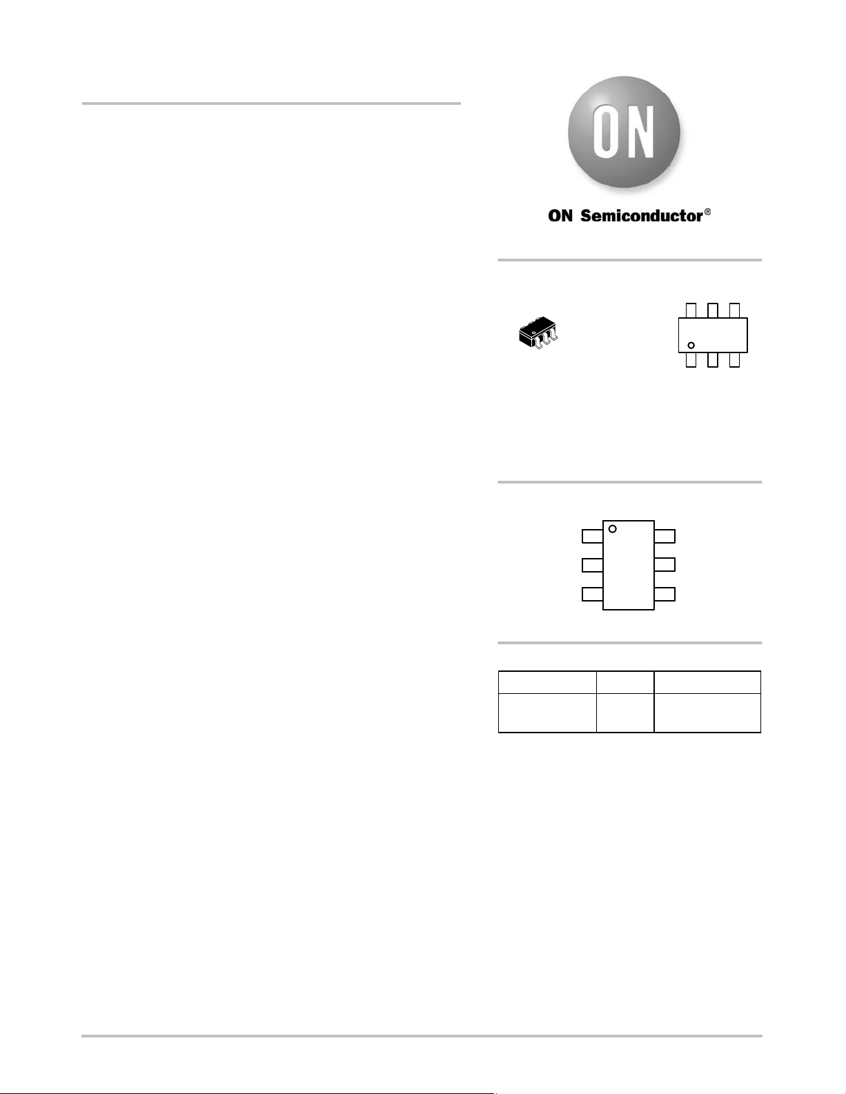
TSOP−6
(SOT23−6, SC59−6)
1
(Note: Microdot may be in either location)
ORDERING INFORMATION
Device Package Shipping
NCL30100SNT1G 3000 / Tape & Reel
†For information on tape and reel specifications,
including part orientation and tape sizes, please
refer to our Tape and Reel Packaging Specifications
Brochure, BRD8011/D.
SN SUFFIX
CASE 318G
AAA = Specific Device Code
A =Assembly Location
Y = Year
W = Work Week
G = Pb−Free Package
PIN CONNECTIONS
1
CS
2GND
CT
3
(Top View)
TSOP−6
(Pb−Free)
6
5
4
AAAAYWG
1
Gate
V
CC
IVC
G
†
© Semiconductor Components Industries, LLC, 2011
January, 2011 − Rev. 3
1 Publication Order Number:
NCL30100/D
6.5 – 24 V
NCL30100
+
C1
IC1
C2
NCL30100
DRV
CS
VCC
GND
IVC
CT
C3
R3
−
R4
R2R1
D1
D2
Q1
LED1
L1
LED2
LEDX
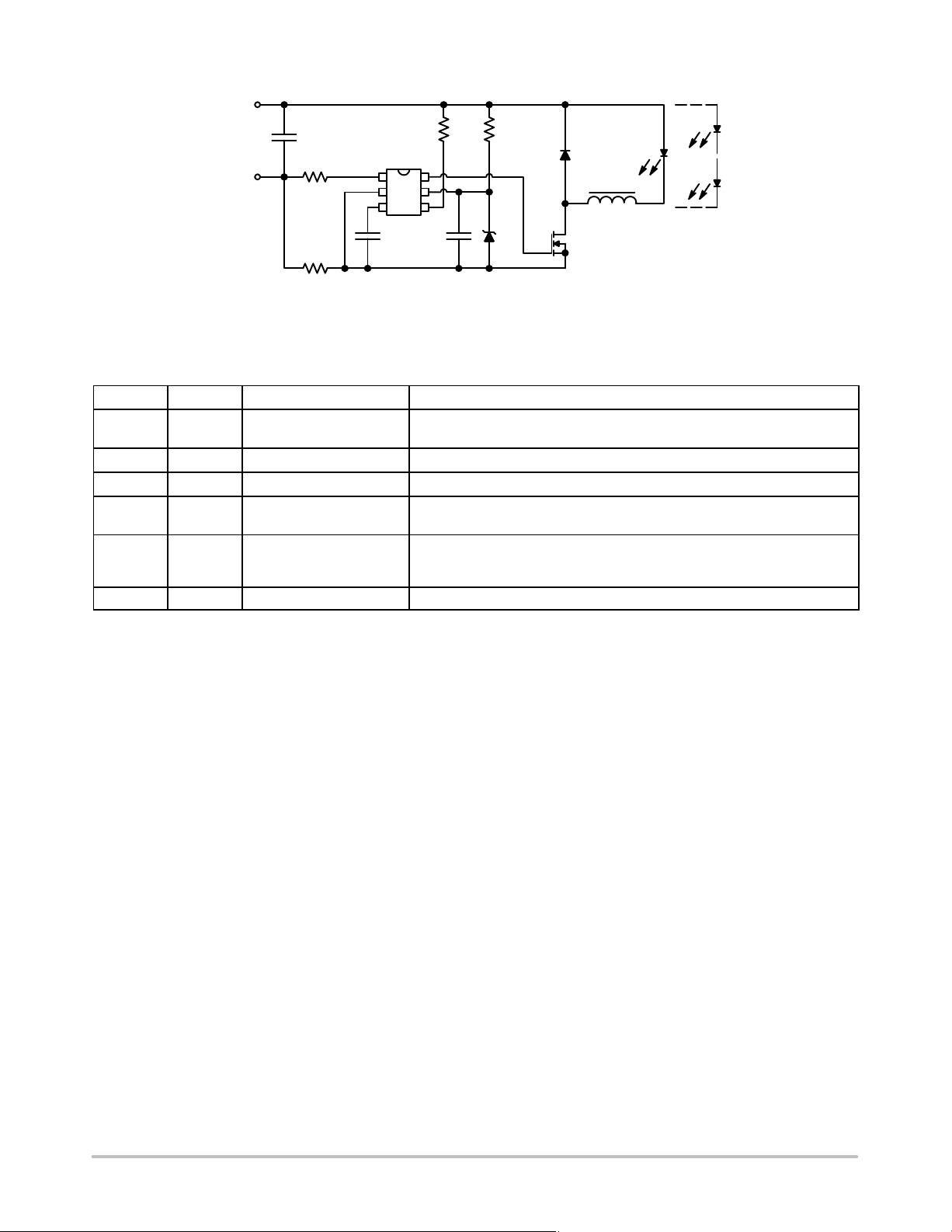
Figure 1. Typical Application Example of the LED Converter
PIN FUNCTION DESCRIPTION
Pin N5 Pin Name Function Pin Description
1 CS Current sense input A resistor divider consisting of R3 and R4 is used to set the peak current
2 GND Ground Power ground.
3 C
T
Timing capacitor Capacitor to establish the off time duration
4 IVC Input voltage compensation The current injected into the input varies the switch off time and I
5 V
CC
Input supply Supply input for the controller. The input is rated to 18 V but as illustrated
6 DRV Driver output Output drive for an external power MOSFET
sensed through the MOSFET switch
feedforward compensation.
Figure 1, a simple zener diode and resistor can allow the LED string to be
powered from a higher voltage
allowing for
PK
http://onsemi.com
2
IVC
Input Voltage
Regulator
NCL30100
VDD
Reference
Iref
Regulator
Undervoltage
Lockout
V
CC
CT
CS
GND
50 mA
12.5−50 mA
Current Sense
Comparator
VOffset
0−3.9 V
OFF Time
Comparator
Reset
Set
S
R
SET
CLR
6.35/5.85 V
Gate Driver
Q
Q
DRV
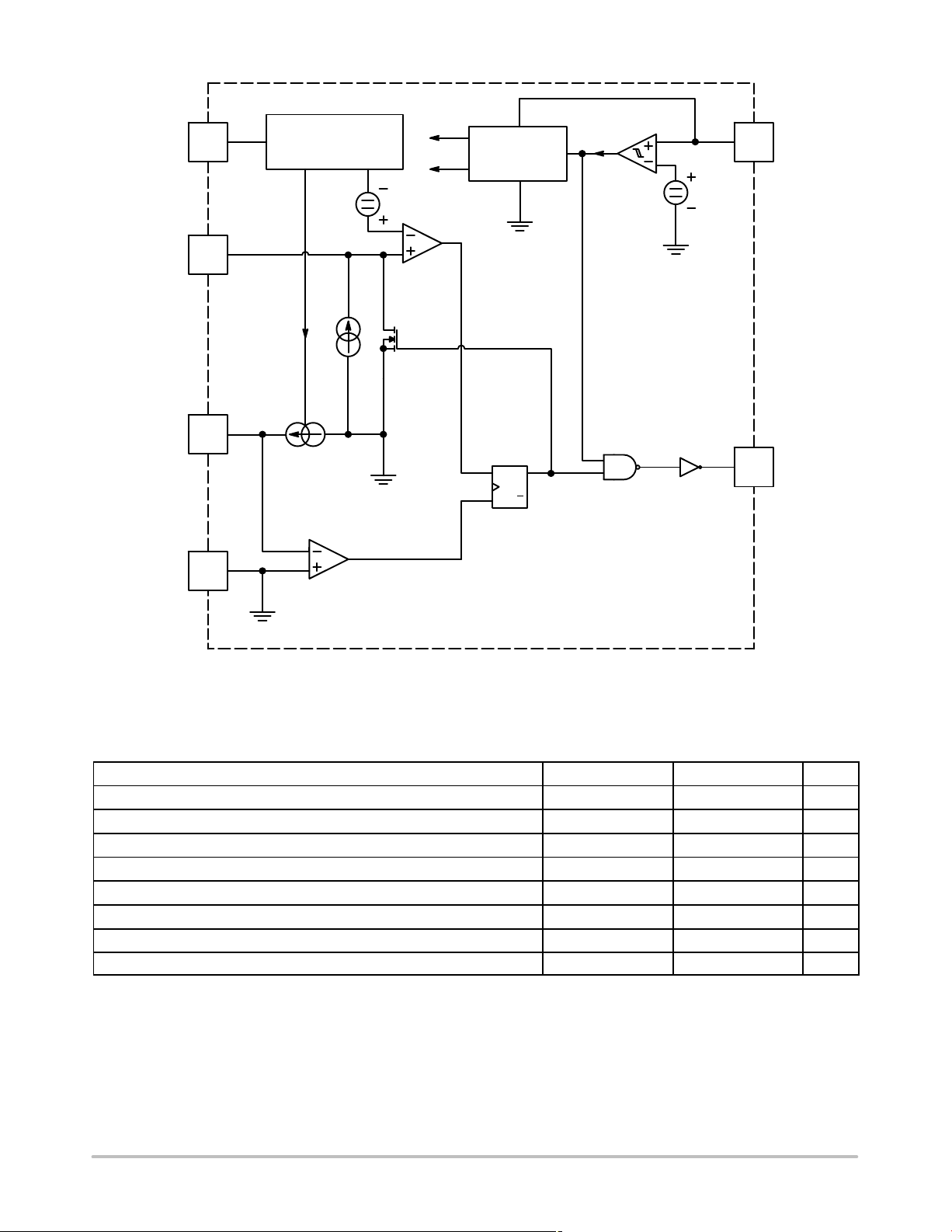
Figure 2. Simplified Circuit Architecture
MAXIMUM RATINGS
Rating Symbol Value Unit
Power Supply Voltage V
CC
IVC Pins Voltage Range IVC −0.3 to 18 V
CS and CT Pin Voltage Range V
Thermal Resistance, Junction−to−Air
Junction Temperature T
Storage Temperature Range T
ESD Voltage Protection, Human Body Model (HBM) V
ESD Voltage Protection, Machine Model (MM) V
in
R
q
JA
J
stg
ESD−HBM
ESD−MM
Stresses exceeding Maximum Ratings may damage the device. Maximum Ratings are stress ratings only. Functional operation above the
Recommended Operating Conditions is not implied. Extended exposure to stresses above the Recommended Operating Conditions may affect
device reliability.
1. This device(s) contains ESD protection and exceeds the following tests:
Human Body Model 2000 V per JEDEC Standard JESD22−A114E
Machine Model 200 V per JEDEC Standard JESD22−A115−A
2. This device meets latchup tests defined by JEDEC Standard JESD78.
3. Moisture Sensitivity Level (MSL) 1.
18 V
−0.3 to 10 V
178 °C/W
150 °C
−60 to +150 °C
2 kV
200 V
http://onsemi.com
3
NCL30100
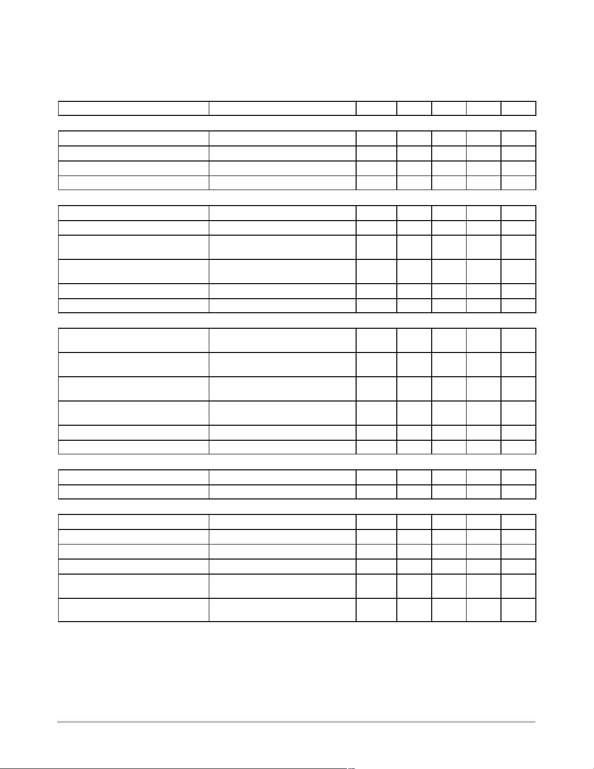
ELECTRICAL CHARACTERISTICS (V
= 12 V, for typical values TJ = 25°C, for min/max values TJ = −40°C to +125°C, unless
CC
otherwise noted)
SUPPLY SECTION
Parameter Conditions Symbol Min Typ Max Unit
INPUT VOLTAGE COMPENSATION
Offset Voltage
CT Pin Voltage
CT Pin Voltage
IVC pin internal resistance (Note 4) R
CT PIN – OFF TIME CONTROL
Source Current
Source Current CT Pin Grounded, −40 v T
Source Current Maximum Voltage Capability (Note 4)
Minimum CT Pin Voltage (Note 4) Pin Unloaded, Discharge Switch TurnedonV
Pin to ground capacitance (Note 4) C
Propagation Delay (Note 4) CT Reach VCT Threshold to Gate Output CT
CURRENT SENSE
Minimum Source Current
Minimum Source Current
Maximum Source Current
Maximum Source Current
Comparator Threshold Voltage (Note 4) V
Propagation Delay CS Falling Edge to Gate Output CS
GATE DRIVER
Sink Resistance
Source Resistance I
POWER SUPPLY
Startup Threshold
Minimum Operating Voltage VCC decreasing V
Vcc Hysteresis (Note 4) V
Startup Current Consumption VCC = 6 V I
Steady State Current Consumption
(Note 4)
Steady State Current Consumption C
4. Guaranteed by design
IVC Current = 25 mA (Including V
IVC Current = 50 mA (Including V
CT Pin Grounded, 0 v T
J
J
IVC = 180 mA, CT Pin Grounded,
0 v T
v 85°C
J
IVC = 180 mA, CT Pin Grounded,
−40 v T
v 125°C
J
IVC = 0 mA, CT Pin Grounded,
0 v T
v 85°C
J
IVC = 0 mA, CT Pin Grounded,
−40 v T
v 125°C
J
I
= 30 mA R
sink
= 30 mA R
source
VCC increasing V
C
= 0 nF, fSW = 100 kHz, IVC = open,
DRV
= 1 nF, fSW = 100 kHz, IVC = open,
DRV
V
= 7 V
CC
V
= 7 V
CC
) V
(offset)
) V
(offset)
v 85°C I
v 125°C I
V
(offset)
CT−25
CT−50mA
IVC
CT
CT
V
CT(max)
CT(min)
CT
delay
I
CS(min)
I
CS(min)
I
CS(max)
I
CS(max)
delay
OL
OH
CC(on)
CC(off)
CC(hyst)
CC1
I
CC2
I
CC2
1.10 1.30 1.45 V
1.69 2.08 2.47 V
mA
2.12 2.6 3.05 V
47.25 50 52.75
45.25 50 52.75
− 4.3 − V
− − 20 mV
− 8 − pF
− 220 − ns
11. 75 12.5 13.25
11.35 12.5 13.25
47.25 50 52.75
45.25 50 52.75
th
− 38 − mV
− 215 310 ns
5 15 40
20 60 100
− 6.35 6.65 V
5.45 5.85 − V
− 0.5 − V
− 22 35
0.5 1 1.15 mA
17
300
kW
mA
mA
mA
mA
mA
mA
W
W
mA
mA
http://onsemi.com
4
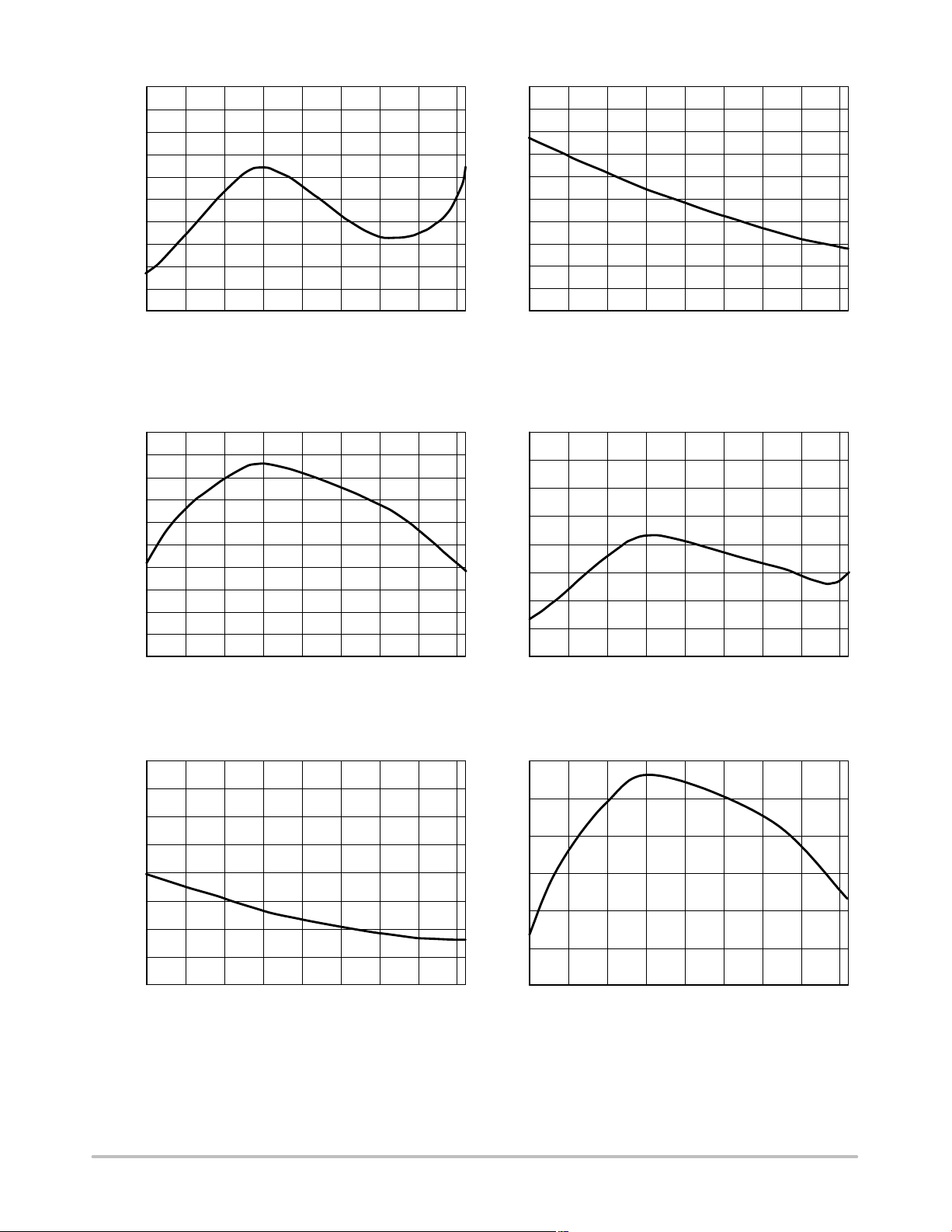
NCL30100
6.260
6.255
6.250
(V)
CC(on)
6.245
V
6.240
6.235
−40 −20 0 20 40 60 80 100 120
TEMPERATURE (°C)
Figure 3. V
Threshold vs. Junction
startup
Temperature
12.6
12.5
12.4
12.3
12.2
(mA)
12.1
12.0
CS(min)
I
11.9
11.8
11.7
11.6
−40 −20 0 20 40 60 80 100 120
TEMPERATURE (°C)
Figure 5. Minimum Source Current vs.
Junction Temperature
30
28
26
24
22
(mA)
20
CC1
I
18
16
14
12
10
−40 −20 0 20 40 60 80 100 120
TEMPERATURE (°C)
Figure 4. Startup Current Consumption vs.
Junction Temperature
5.780
5.775
5.770
5.765
(V)
5.760
CC(off)
5.755
V
5.750
5.745
5.740
−40 −20 0 20 40 60 80 100 120
TEMPERATURE (°C)
Figure 6. Minimum Operating Voltage
Threshold vs. Junction temperature
1.10
1.05
(mA)
1.00
CC2
I
0.95
0.90
−40 −20 0 20 40 60 80 100 120
TEMPERATURE (°C)
Figure 7. Steady State Current Consumption
vs. Junction Temperature
50.0
49.5
49.0
(mA)
48.5
CS(max)
I
48.0
47.5
47.0
http://onsemi.com
5
−40 −20 0 20 40 60 80 100 120
TEMPERATURE (°C)
Figure 8. Maximum Source Current vs.
Junction Temperature
NCL30100
55
50
45
40
(mV)
th
V
35
30
25
−40 −20 0 20 40 60 80 100 120
TEMPERATURE (°C)
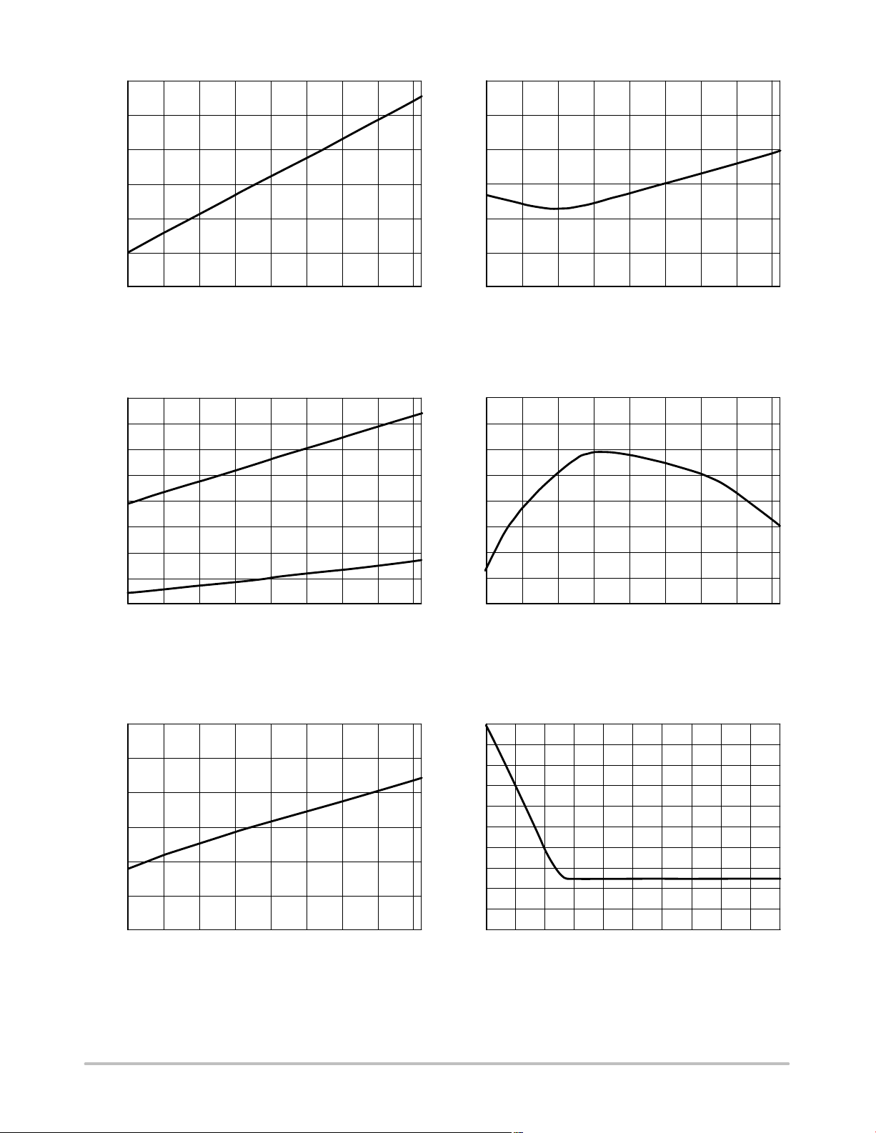
Figure 9. Comparator Threshold Voltage vs.
Junction Temperature
85
75
65
R
55
OH
1.350
1.345
1.340
(V)
1.335
(offset)
V
1.330
1.325
1.320
−40 −20 0 20 40 60 80 100 120
TEMPERATURE (°C)
Figure 10. Offset Voltage vs. Junction
Temperature
51.0
50.5
50.0
49.5
45
35
RESISTANCE (W)
25
R
15
5
−40 −20 0 20 40 60 80 100 120
OL
TEMPERATURE (°C)
Figure 11. Drive Sink and Source Resistance
vs. Junction Temperature
2.60
2.55
2.50
(V)
A
m
2.45
CT−50
V
2.40
2.35
2.30
−40 −20 0 20 40 60 80 100 120
TEMPERATURE (°C)
Figure 13. CT Pin Voltage vs. Input Voltage
Compensation Current
49.0
(mA)
CT
I
48.5
48.0
47.5
47.0
−40 −20 0 20 40 60 80 100 120
TEMPERATURE (°C)
Figure 12. CT Source Current vs. Junction
Temperature
50
45
40
35
30
25
(mA)
CS
I
20
15
10
5
0
0 20 20018016014012040 60 80 100
IVC (mA)
Figure 14. ICT Dependence on IVC Current
http://onsemi.com
6
NCL30100
APPLICATION INFORMATION
The NCL30100 implements a peak current mode control
scheme with a quasi−fixed OFF time. An optional input
feedforward voltage control is provided to enhance
regulation response with widely varying input voltages.
Only a few external components are necessary to implement
the buck converter. The NCL30100 incorporates the
following features:
• Very Low Startup Current: The patented internal supply
block is specially designed to offer a very low current
consumption during startup.
• Negative Current Sensing: By sensing the total current,
this technique does not impact the MOSFET driving
voltage (V
) during switching. Furthermore, the
GS
programming resistor together with the pin capacitance
forms a residual noise filter which blanks spurious
spikes. This approach also supports a flexible resistor
selection. Finally unlike a positive sensing approach,
there is virtually no power dissipation in the current
sense resistor thus improving efficiency.
• Controller architecture supports high brightness LED
drive current requirements: Selection of the external
n−channel MOSFET can be easily optimized based on
operation voltage, drive current and size giving the
designer flexibility to easily make design tradeoffs.
• Typical $5.5% Current Regulation: The I
pin offers
CS
$5.5% from 0 to 85°C (+5.5% −9.5% across −40°C to
125°C) accuracy of the current typically, so the LED
peak current is precisely controlled
• No output capacitor is needed: By operating the
controller in continuous conduction mode, it is possible
to eliminate the bulky output filter capacitor.
The following section describes in detail each of the control
blocks
the switch and the inductor. This approach offers several
benefits over traditional positive current sensing.
• Maximum peak voltage across the current sense resistor
is user controlled and can be optimized by changing the
value of the shift resistor.
• The gate drive capability is improved because the
current sense resistor is located out of the gate driver
loop and does not deteriorate the switch on and also
switch off gate drive amplitude.
• Natural leading edge blanking is filter switching noise
at FET turn−in
• The CS pin is not exposed to negative voltage, which
could induce a parasitic substrate current within the IC
and distort the surrounding internal circuitry.
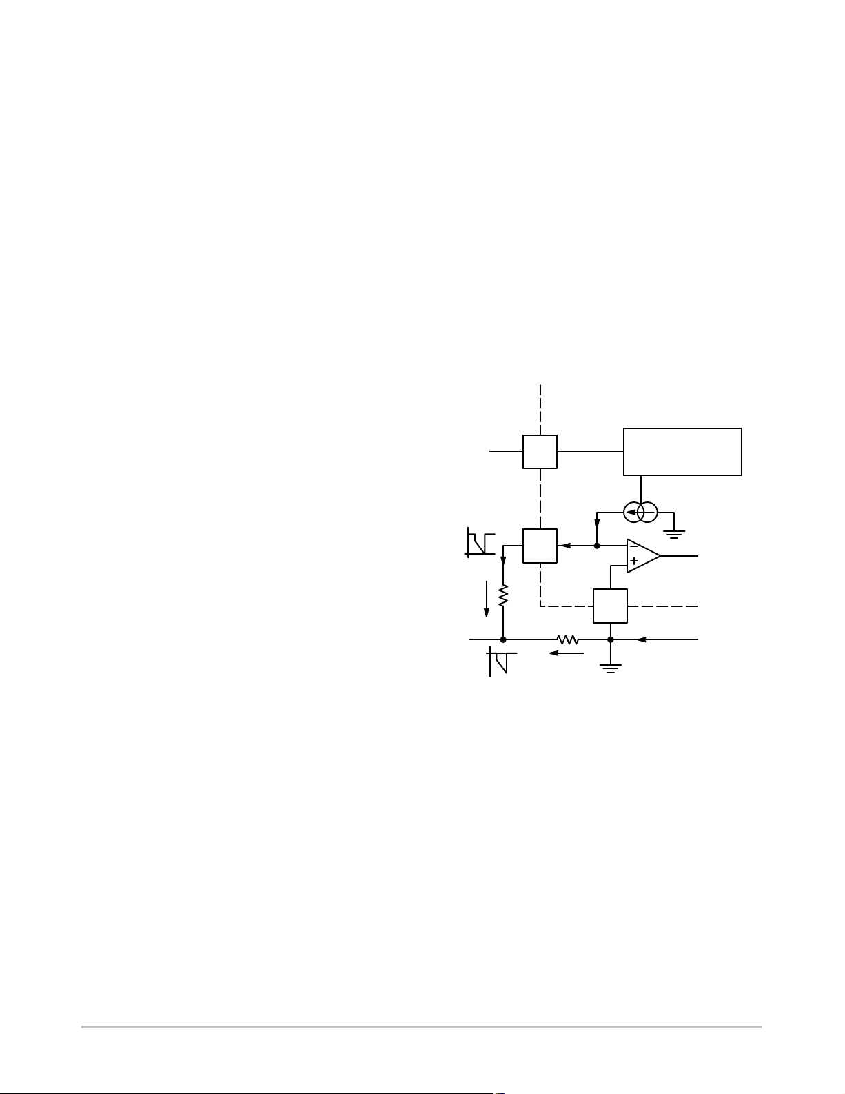
The current sensing circuit is shown in Figure 15.
IVC
Input Voltage
Regulator
12.5−50 mA
CS
To Latch
Vshift
Rshift
RCS
VCS
GND
Iprimary
Current Sensing Block
The NCL30100 utilizes a technique called negative
current sensing which is used to set the peak current through
http://onsemi.com
Figure 15. Primary Current Sensing
7
NCL30100
Once the external MOSFET is switched on, the inductor
current starts to flow through the sense resistor R
current creates a voltage drop V
on the resistor RCS, which
CS
CS
. The
is negative with respect to GND. Since the comparator
connected to CS pin requires a positive voltage, a voltage
V
is developed across the resistor R
shift
source which level−shifts the negative voltage V
by a current
shift
CS
. The
level−shift current is in the range from 12.5 to 50 mA
depending on the optional input voltage compensation loop
control block signal (see more details in the input voltage
compensation section). The peak inductor current is equal
to:
I
@ R
* V
Ipk+
R
shift
CS
To achieve the best Ipk precision, higher values of I
CS
th
(eq. 1)
CS
should be used. The Equation 1 shows the higher drop on
R
reduces the influence of the Vth tolerance. Vth is the
CS
comparator threshold which is nominally 38 mV.
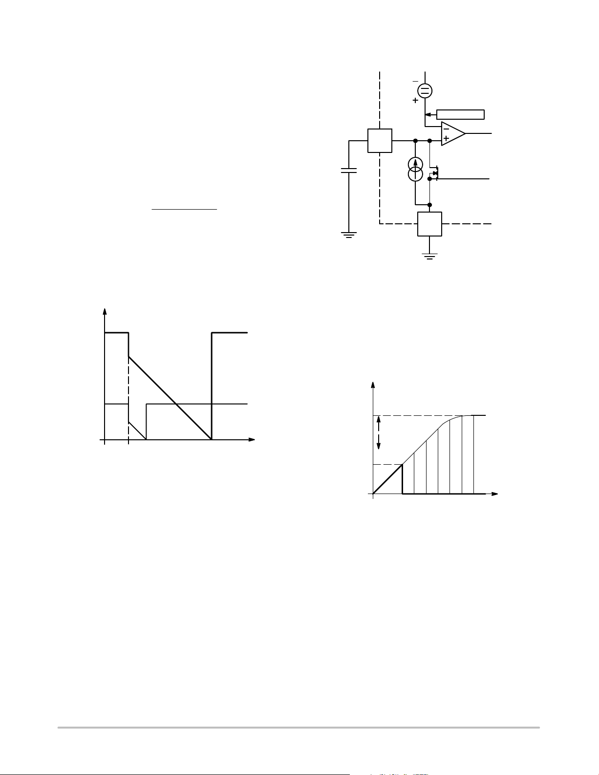
A typical CS pin voltage waveform for continuous
condition mode is shown in Figure 16.
V
I
shift = 50 mA
From Input Voltage
Compensation Block
VOffset
VOffset to VDD
CT
CT
50 mA
To Latch’s Set Input
To Latch’s Output
GND
Figure 17. OFF Time Control
During the switch−on time, the CT capacitor is kept
discharged by an internal switch. As soon as the latch output
changes to a low state, the I
across C
threshold given by the V
starts to ramp−up until its value reaches the
T
offset
is enabled and the voltage
source
. The current injected into IVC
can change this threshold. The IVC operation will be
discussed in the next section.
shift = 12.5 mA
I
0
Switch
Turn on
t
Figure 16. CS Pin Voltage
Figure 16 also shows the effect of the inductor current
based on the range of control possible via the IVC input.
OFF Time Control
The internal current source, together with an external
capacitor, controls the switch−off time. In addition, the
optional IVC control signal can modulate the off time based
on input line voltage conditions. This block is illustrated in
Figure 17.
V
VDD
Goes Up
I
CT pin
Voltage
Voffset
VC
Goes Down
I
VC
I3
I2
t
off−min
I1
t
0
Figure 18. CT Pin Voltage
The voltage that can be observed on CT pin is shown in
Figure 18. The bold line shows the minimum IVC current
when the off time is at its minimum. The amount of current
injected into the IVC input can increase the off time by
changing the turn off comparator switching threshold. I1, I2,
http://onsemi.com
8
NCL30100
and I3 represent different delays depending on the
magnitude of IVC.
V
CC
Gate Driver
The Gate Driver consists of a CMOS buffer designed to
directly drive a power MOSFET. It features unbalanced
source and sink capabilities to optimize switch on and off
performance without additional external components. The
power MOSFET is switched off at high drain current, to
minimize its switch off losses the sink capability of the gate
driver is increased for a faster switch off. On the other hand,
the source capability of the driver is reduced to slow−down
the power MOSFET at switch on in order to reduce EMI
generation. Whenever the IC supply voltage is lower than
the under voltage threshold, the Gate Driver is low, pulling
down the gate to ground thus eliminating the need for an
external resistor.
Input Voltage Compensation:
The Input Voltage Compensation block gives the user
optional flexibility to sense the input voltage and modify the
current sense threshold and off time. This function provides
a feed forward mechanism that can be used when the input
voltage of the controller is loosely regulated to improve
output current regulation. If the input voltage is well
regulated, the IVC input can also be used to adjust the offset
of the off time comparator and the current sense control to
achieve the best current regulation accuracy.
An external resistor connected between IVC and the input
supply results in a current being injected into this pin which
has an internal 17 kW resistor connected to a current mirror.
This current information is used to modify V
By changing V
the off time comparator threshold is
offset
offset
and ICS.
modified and the off time is increased. A small capacitor
should be connected between the IVC pin and ground to
filter out noise generated during switching period. Figure 19
shows the simplified internal schematic:
Current
Mirror
1:1
25 kW
VOffset
To OFF
Time
Comparator
mA
17 kW
IVC
Current
Mirror
1:1
Figure 19. Input Voltage Compensation, OFF Time
Control
V
VDD
Voltage
Voffset
OFF Time Comparator Input
0
IVC Pin Sink Current
Figure 20. IVC Loop Transfer Characteristic
The transfer characteristic (output voltage to input
current) of the input voltage compensation loop control
block can be seen in Figure 20. V
refers to the internal
DD
stabilized supply. If no IVC current is injected, the off time
comparator is set to V
offset
.
The value of the current injected into IVC also change Ics.
This is accomplished by changing the voltage drop on R
shift
The corresponding block diagram of the IVC pin can be seen
in Figure 21.
.
To Current Sense Comparator
17 kW
IVC
Current
Mirror
4:3
Figure 21. Input Voltage Compensation Loop – Current Sense Control
http://onsemi.com
9
37.5 mA
CS
12.5 mA
 Loading...