

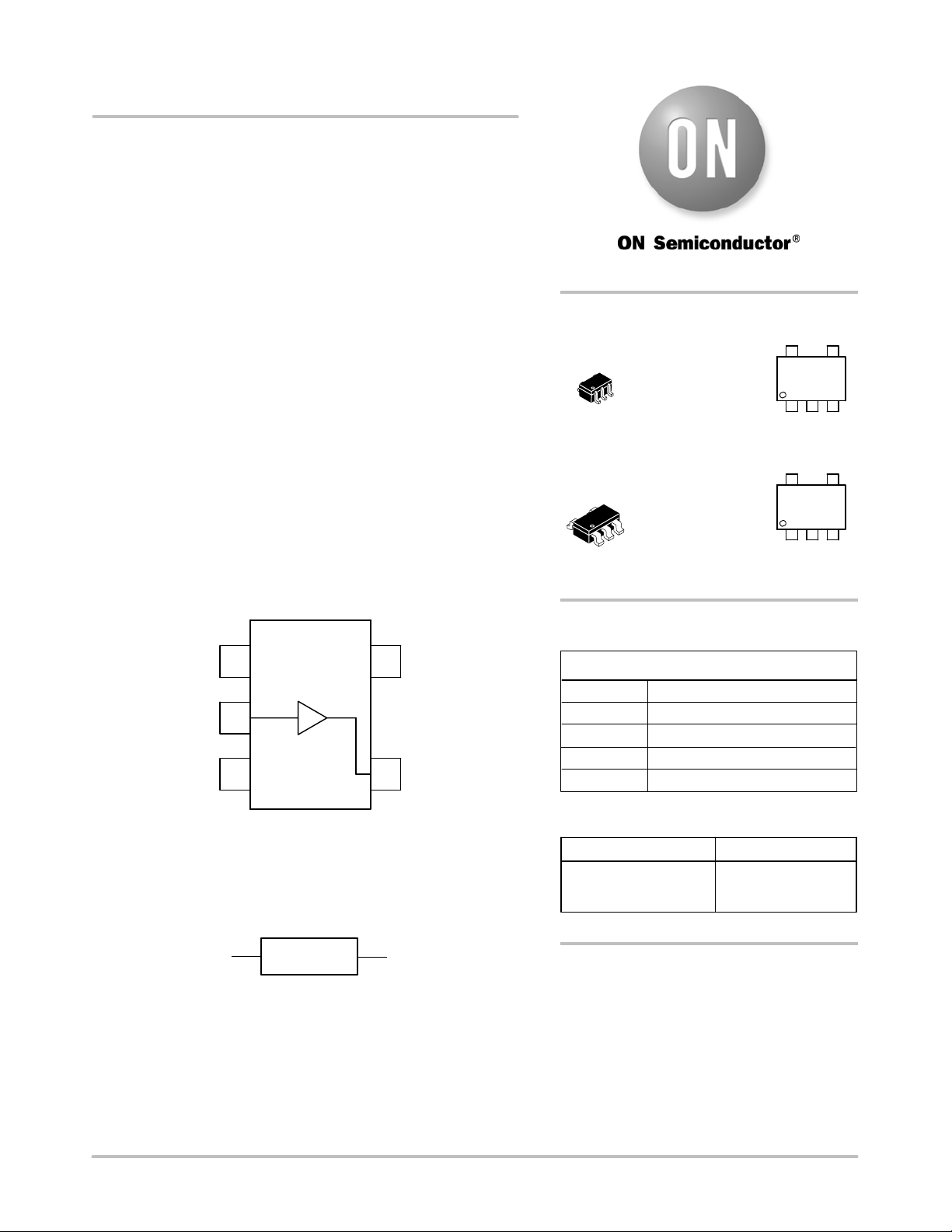
MC74VHC1G50
Buffer
The MC74VHC1G50 is an advanced high speed CMOS buffer
fabricated with silicon gate CMOS technology. It achieves high speed
operation similar to equivalent Bipolar Schottky TTL while maintaining
CMOS low power dissipation.
The internal circuit is composed of three stages, including a buffered
output which provides high noise immunity and stable output.
The MC74VHC1G50 input structure provides protection when
voltages up to 7.0 V are applied, regardless of the supply voltage. This
allows the MC74VHC1G50 to be used to interface 5.0 V circuits to 3.0 V
circuits.
• High Speed: t
• Low Power Dissipation: I
• Power Down Protection Provided on Inputs
• Balanced Propagation Delays
• Pin and Function Compatible with Other Standard Logic Families
• Chip Complexity: FET = 104; Equivalent Gate = 26
• These devices are available in Pb--free package(s). Specifications herein
apply to both standard and Pb--free devices. Please see our website at
www.onsemi.com for specific Pb--free orderable part numbers, or
contact your local ON Semiconductor sales office or representative.
= 3.5 ns (Typ) at VCC=5V
PD
=1mA(Max)atTA=25°C
CC
http://onsemi.com
SC--88A / SOT--353/SC--70
DF SUFFIX
CASE 419A
TSOP-- 5/SOT--23/SC--59
DT SUFFIX
CASE 483
MARKING
DIAGRAMS
d
VR
Pin 1
d = Date Code
d
VR
Pin 1
d = Date Code
1
NC
IN A
2
3
GND
Figure 1. Pinout (Top View)
IN A
1
Figure 2. Logic Symbol
5
4
OUT Y
V
CC
OUT Y
PIN ASSIGNMENT
1
2
3GND
4
5V
NC
IN A
OUT Y
CC
FUNCTION TABLE
A Input Y Output
L
H
L
H
ORDERING INFORMATION
See detailed ordering and shippinginformation in the package
dimensions section on page 4 of this data sheet.
© Semiconductor Components Industries, LLC, 2006
March, 2006 -- Rev. 12
1 Publication Order Number:
MC74VHC1G50/D
MC74VHC1G50
MAXIMUM RATINGS (Note 1)
Symbol
V
CC
V
IN
V
OUT
I
IK
I
OK
I
OUT
I
CC
P
D
θ
JA
T
L
T
J
T
stg
V
ESD
I
Latch--Up
DC Supply Voltage --0.5to+7.0 V
DC Input Voltage --0.5to+7.0 V
DC Output Voltage VCC=0
Input Diode Current -- 2 0 mA
Output Diode Current V
DC Output Current, per Pin +25 mA
DC Supply Current, VCCand GND +50 mA
Power dissipation in still air SC--88A, TSOP-- 5 200 mW
Thermal resistance SC--88A, TSOP--5 333 °C/W
Lead temperature, 1 mm from case for 10 s 260 °C
Junction temperature under bias +150 °C
Storage temperature --65 to +150 °C
ESD Withstand Voltage Human Body Model (Note 2)
Latch--Up Performance Above VCCand Below GND at 125°C(Note5) ±500 mA
1. Maximum Ratings are those values beyond which damage to the device may occur.Exposure to these conditions or conditions beyond those
indicated may adversely affect device reliability. Functional operation under absolute--maximum--rated conditions is not implied. Functional
operation should be restricted to the Recommended Operating Conditions.
2. Tested to EIA/JESD22--A114--A
3. Tested to EIA/JESD22--A115--A
4. Tested to JESD22--C101--A
5. Tested to EIA/JESD78
Characteristics Value Unit
High or Low State
< GND; V
OUT
OUT>VCC
Machine Model (Note 3)
Charged Device Model (Note 4)
--0.5to7.0
--0.5toV
CC
+0.5
+20 mA
> 2000
> 200
N/A
V
V
RECOMMENDED OPERATING CONDITIONS
Symbol Characteristics Min Max Unit
V
CC
V
IN
V
OUT
T
A
tr,t
DC Supply Voltage 2.0 5.5 V
DC Input Voltage 0.0 5.5 V
DC Output Voltage 0.0 V
CC
Operating Temperature Range -- 5 5 +125 °C
Input Rise and Fall Time VCC=3.3V± 0.3 V
f
V
=5.0V± 0.5 V
CC
0
0
100
20
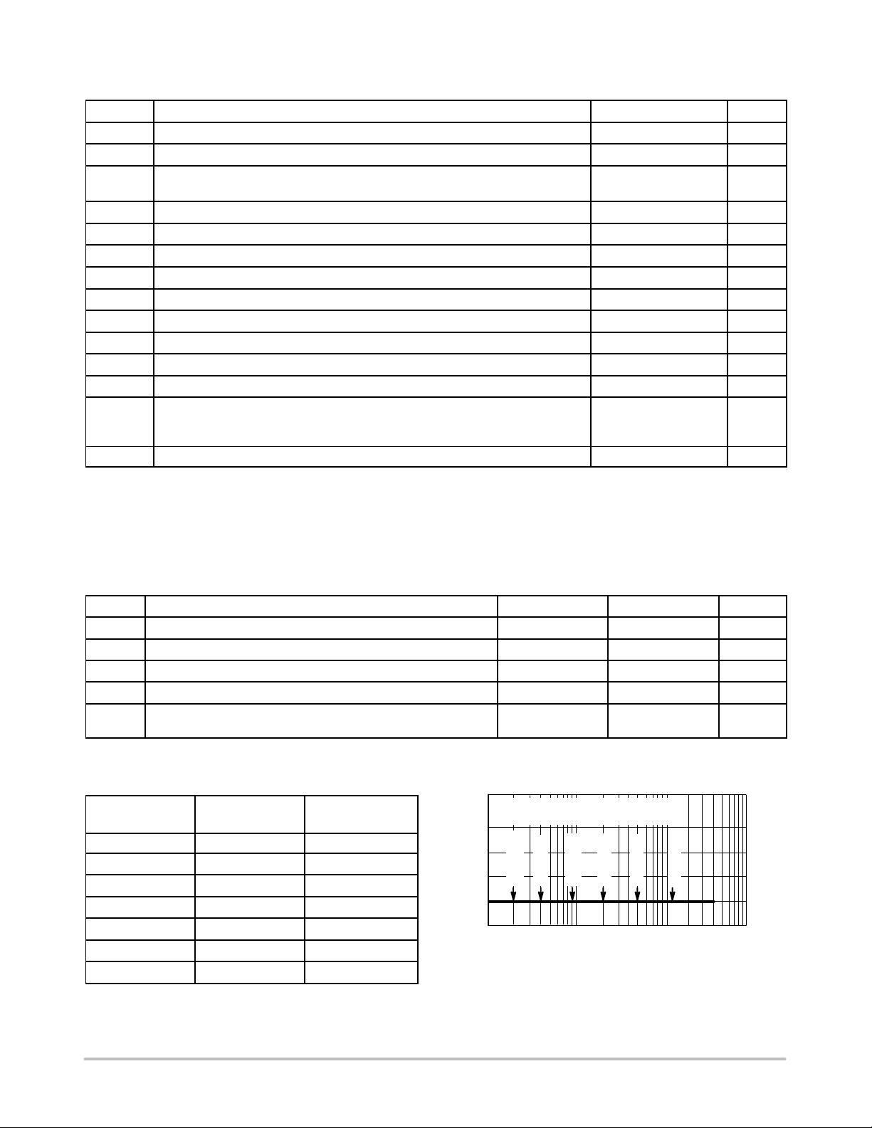
Device Junction Temperature versus
Time to 0.1% Bond Failures
Junction
Temperature °C
Time, Hours Time, Years
80 1,032,200 117.8
90 419,300 47.9
100 178,700 20.4
110 79,600 9.4
120 37,000 4.2
130 17,800 2.0
140 8,900 1.0
FAILURE RATE OF PLASTIC = CERAMIC
UNTIL INTERMETALLICS OCCUR
= 130 C°
J
T
J
J
T
T
=110 C°
= 120 C°
1
NORMALIZED FAILURE RATE
1 10 100
TIME, YEARS
Figure 3. Failure Rate vs. Time
C°
C°
=80
=90
= 100 C°
J
T
J
J
T
T
1000
Junction Temperature
V
ns/V
http://onsemi.com
2
DC ELECTRICAL CHARACTERISTICS
Symbol Parameter Test Conditions
V
IH
V
IL
V
OH
V
OL
I
IN
I
CC
Minimum High--Level
Input Voltage
Maximum Low--Level
Input Voltage
Minimum High--Level
Output Voltage
IN=VIH
or V
IL
V
Maximum Low--Level
Output Voltage
IN=VIH
or V
IL
V
Maximum Input
Leakage Current
Maximum Quiescent
Supply Current
VIN=VIHor V
IOH=--50mA
VIN=VIHor V
IOH=--4mA
=--8mA
I
OH
VIN=VIHor V
IOL=50mA
VIN=VIHor V
IOL=4mA
=8mA
I
OL
IL
IL
IL
IL
VIN=5.5VorGND 0to
VIN=VCCor GND 5.5 1.0 20 40
MC74VHC1G50
V
CC
(V)
2.0
3.0
4.5
5.5
2.0
3.0
4.5
5.5
2.0
3.0
4.5
3.0
4.5
2.0
3.0
4.5
3.0
4.5
5.5
TA=25°C TA≤ 85°C -- 5 5 ≤ TA≤ 125°C
Min Typ Max Min Max Min Max
1.5
2.1
3.15
3.85
1.9
2.0
2.9
3.0
4.4
4.5
2.58
3.94
0.0
0.0
0.0
0.5
0.9
1.35
1.65
0.1
0.1
0.1
0.36
0.36
1.5
2.1
3.15
3.85
0.5
0.9
1.35
1.65
1.9
2.9
4.4
2.48
3.80
0.1
0.1
0.1
0.44
0.44
1.5
2.1
3.15
3.85
0.5
0.9
1.35
1.65
1.9
2.9
4.4
2.34
3.66
0.1
0.1
0.1
0.52
0.52
±0.1 ±1.0 ±1.0
Unit
V
V
V
V
V
V
mA
mA
AC ELECTRICAL CHARACTERISTICS C
= 50 pF, Input tr=tf=3.0ns
load
TA=25°C TA≤ 85°C -- 5 5 ≤ TA≤ 125°C
Symbol Parameter Test Conditions
t
PLH
t
PHL
,
Maximum Propagation Delay,
Input A to
Y
VCC=3.3± 0.3 V CL=15pF
C
VCC=5.0± 0.5 V CL=15pF
C
C
IN
Maximum Input Capacitance
=50pF
L
=50pF
L
Min Typ Max Min Max Min Max
4.5
6.4
3.5
4.5
7.1
10.6
5.5
7.5
8.5
12.0
6.5
8.5
10.0
14.5
8.0
10.0
4 10 10 10 pF
Unit
ns
Typical @ 25°C, VCC=5.0V
C
PD
Power Dissipation Capacitance (Note 6)
8.0
pF
6. CPDis defined as the value of the internal equivalent capacitance which is calculated from the operating current consumption without load.
Average operating current can be obtained by the equation: I
power consumption; P
D=CPD
¯ V
CC
2
¯ fin+ICC¯ VCC.
=CPD¯ VCC¯ fin+ICC.CPDis used to determine the no --load dynamic
)
CC(OPR
http://onsemi.com
3

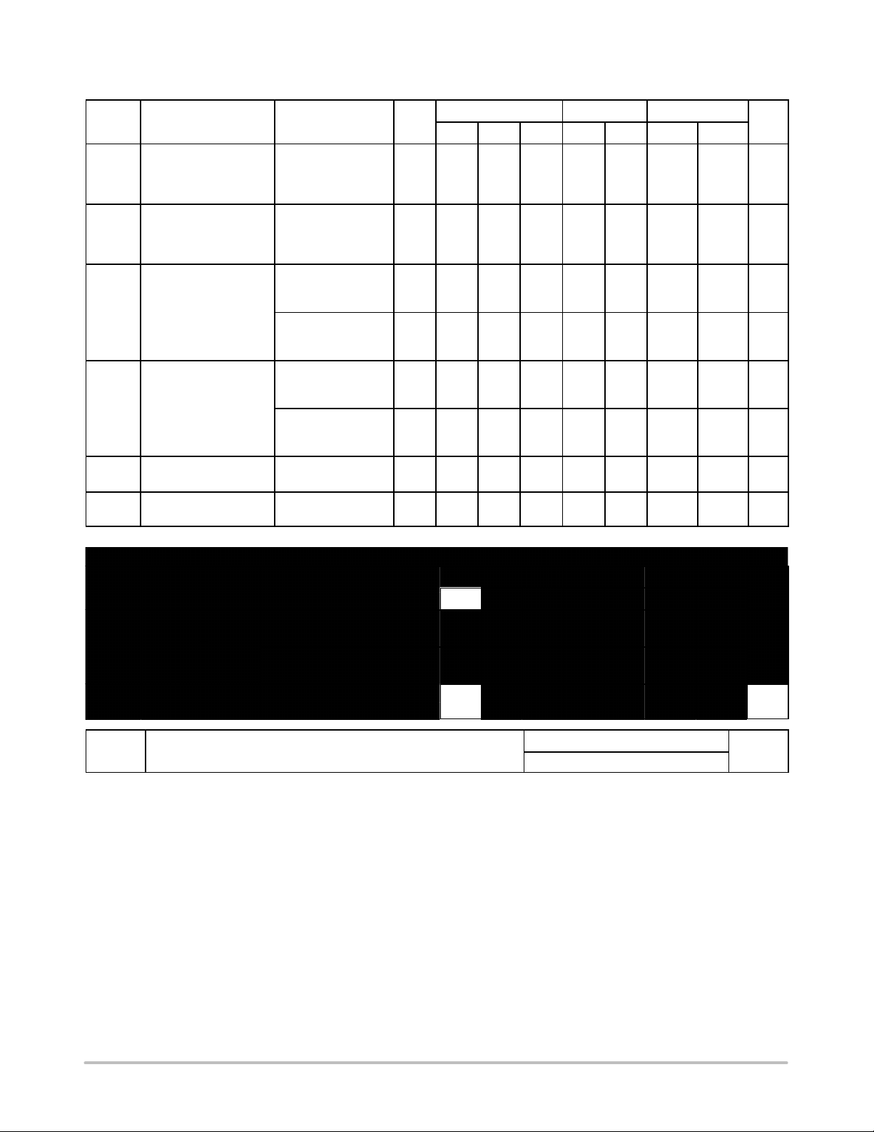
AorB
50%
t
PHL
t
PLH
MC74VHC1G50
V
CC
GND
DEVICE
UNDER
TEST
TEST POINT
OUTPUT
CL*
Y
50% V
CC
*Includes all probe and jig capacitance
Figure 4. Switching Waveforms Figure 5. Test Circuit
DEVICE ORDERING INFORMATION
Device Nomenclature
Tem p
Device Order Number
Circuit
Indicator
Range
Identifier
Technology
Device
Function
Package
Suffix
MC74VHC1G50DFT1 MC 74 VHC1G 50 DF T1
MC74VHC1G50DFT2 MC 74 VHC1G 50 DF T2
MC74VHC1G50DTT1 MC 74 VHC1G 50 DT T1
†For information on tape and reel specifications, including part orientation and tape sizes, please refer to our Tape and Reel Packaging
Specifications Brochure, BRD8011/D.
Tap e &
Reel
Suffix
Package Type
SC--88A /
SOT--353 / SC--70
SC--88A /
SOT--353 / SC--70
TSOP-- 5 / SOT--23
/SC--59
Tap e an d
Reel Size
178 mm (7”)
3000 Unit
178 mm (7”)
3000 Unit
178 mm (7”)
3000 Unit
†
http://onsemi.com
4

MC74VHC1G50
CAVITY
TAPE
TOP TAPE
TAPE DIMENSIONS mm
8.00 ±0.30
TAPE TRAILER
(Connected to Reel Hub)
NO COMPONENTS
160 mm MIN
COMPONENTS
DIRECTION OF FEED
TAPE LEADER
NO COMPONENTS
Figure 6. Tape Ends for Finished Goods
4.00
2.00
4.00
∅1.00 MIN
1
DIRECTION OF FEED
Figure 7. SC--70--5/SC--88A/SOT --353 DFT1 Reel Configuration/Orientation
400 mm MIN
∅1.50 TYP
1.75
3.50 ±0.50
TAPE DIMENSIONS mm
2.00
8.00 ±0.30
4.00
4.00
∅1.00 MIN
∅1.50 TYP
1.75
3.50 ±0.50
1
DIRECTION OF FEED
Figure 8. SC--70/SC--88A/SOT--353 DFT2 and SOT23--5/TSOP --5/SC59--5 DTT1 Reel Configuration/Orientation
http://onsemi.com
5

MC74VHC1G50
13.0 mm ±0.2 mm
1.5 mm MIN
(0.06 in)
(0.512 in ±0.008 in)
tMAX
20.2 mm MIN
A
(0.795 in)
REEL DIMENSIONS
Tap e Si z e
8mm
T and R Suffix
T1, T2
FULL RADIUS
Figure 9. Reel Dimensions
AMax
178 mm
(7 in)
DIRECTION OF FEED
8.4 mm, + 1.5 mm, --0.0
(0.33 i n + 0.059 in, --0.00)
50 mm MIN
(1.969 in)
G
G
tMax
14.4 mm
(0.56 in)
BARCODE LABEL
Figure 10. Reel Winding Direction
http://onsemi.com
6
HOLEPOCKET

MC74VHC1G50
PACKAGE DIMENSIONS
SC70--5/SC--88A/SOT--353
DF SUFFIX
5--LEAD PACKAGE
CASE 419A--02
A
G
45
S
12 3
-- B --
MM
D
5PL
B0.2 (0.008)
N
ISSUE G
J
NOTES:
1. DIMENSIONING AND TOLERANCING
PER ANSI Y14.5M, 1982.
2. CONTROLLING DIMENSION: INCH.
3. 419A--01 OBSOLETE. NEW STANDARD
419A--02.
4. DIMENSIONS A AND B DO NOT INCLUDE
MOLD FLASH, PROTRUSIONS, OR GATE
BURRS.
INCHES
DIMAMIN MAX MIN MAX
B 1.15 1.350.045 0.053
C 0.80 1.100.031 0.043
D 0.10 0.300.004 0.012
G 0.65 BSC0.026 BSC
H -- -- -- 0 . 1 0-- -- --0.004
J 0.10 0.250.004 0.010
K 0.10 0.300.004 0.012
N 0.20 REF0.008 REF
S 2.00 2.200.079 0.087
MILLIMETERS
1.80 2.200.071 0.087
K
SOLDERING FOOTPRINT*
0.50
0.0197
0.65
0.025
0.65
0.025
0.40
0.0157
1.9
SCALE 20:1
0.0748
Figure 11. SC--88A/SC70--5/SOT--353
*For additional information on our Pb--Free strategy and soldering
details, please download the ON Semiconductor Soldering and
Mounting Techniques Reference Manual, SOLDERRM/D.
mm
inches
http://onsemi.com
7

0.05 (0.002)
S
H
D
54
123
L
G
A
MC74VHC1G50
PACKAGE DIMENSIONS
SOT23--5/TSOP--5/SC59--5
DT SUFFIX
5--LEAD PACKAGE
CASE 483--01
ISSUE C
B
J
C
K
M
SOLDERING FOOTPRINT*
1.9
0.95
0.037
0.074
NOTES:
1. DIMENSIONING AND TOLERANCING PER
ANSI Y14.5M, 1982.
2. CONTROLLING DIMENSION: MILLIMETER.
3. MAXIMUM LEAD THICKNESS INCLUDES
LEAD FINISH THICKNESS. MINIMUM LEAD
THICKNESS IS THE MINIMUM THICKNESS
OF BASE MATERIAL.
4. A AND B DIMENSIONS DO NOT INCLUDE
MOLD FLASH, PROTRUSIONS, OR GATE
BURRS.
DIM MIN MAX MIN MAX
A 2.90 3.10 0.1142 0.1220
B 1.30 1.70 0.0512 0.0669
C 0.90 1.10 0.0354 0.0433
D 0.25 0.50 0.0098 0.0197
G 0.85 1.05 0.0335 0.0413
H 0.013 0.100 0.0005 0.0040
J 0.10 0.26 0.0040 0.0102
K 0.20 0.60 0.0079 0.0236
L 1.25 1.55 0.0493 0.0610
M 010 0 10
__ _ _
S 2.50 3.00 0.0985 0.1181
INCHESMILLIMETERS
2.4
0.094
1.0
0.039
mm
0.7
0.028
SCALE 10:1
inches
Figure 12. THIN SOT23--5/TSOP--5/SC59--5
*For additional information on our Pb--Free strategy and soldering
details, please download the ON Semiconductor Soldering and
Mounting Techniques Reference Manual, SOLDERRM/D.
ON Semiconductor and are registered trademarks of Semiconductor Components Industries, LLC (SCILLC). SCILLC reserves the right to make changes without further notice
to any products herein. SCILLC makes no warranty, representation or guarantee regarding the suitability of its products for any particular purpose, nor does SCILLC assume any liability
arising out of the application or use of any product or circuit, and specifically disclaims any and all liability, including without limitation special, consequential or incidental damages.
“Typical” parameters which may be provided in SCILLC data sheets and/or specifications can and do vary in different applications and actual performance may vary over time. All
operating parameters, including “Typicals”must be validated for each customer application by customer’s technical experts. SCILLC does not convey any license under its patent rights
nor the rights of others. SCILLC products are not designed, intended, or authorized for use as components in systems intended for surgical implant into the body, or other applications
intended to support or sustain life, or for any other application in which the failure of the SCILLC product could create a situation where personal injury or death may occur. Should
Buyer purchase or use SCILLC products for any such unintended or unauthorized application, Buyer shall indemnifyand hold SCILLC and its officers, employees, subsidiaries, affiliates,
and distributors harmless against all claims, costs, damages, and expenses, and reasonable attorney fees arising out of, directly or indirectly, any claim of personal injury or death
associated with such unintended or unauthorized use, even if such claim alleges that SCILLC was negligent regarding the design or manufacture of the part. SCILLC is an Equal
Opportunity/Affirmative Action Employer. This literature is subject to all applicable copyright laws and is not for resale in any manner.
PUBLICATION ORDERING INFORMATION
LITERATURE FULFILLMENT:
Literature Distribution Center for ON Semiconductor
P.O. Box 61312, Phoenix, Arizona 85082--1312 USA
Phone: 480--829--7710 or 800 --344--3860 Toll Free USA/Canada
Fax: 480--829--7709 or 800 --344--3867 Toll Free USA/Canada
Email: orderlit@onsemi.com
N. American Technical Support: 800--282--9855 Toll Free
USA/Canada
Japan: ON Semiconductor, Japan Customer Focus Center
2--9--1 Kamimeguro, Meguro--ku, Tokyo, Japan 153--0051
Phone: 81--3--5773--3850
http://onsemi.com
8
ON Semiconductor Website: http://onsemi.com
Order Literature: http://www.onsemi.com/litorder
For additional information, please contact your
local Sales Representative.
MC74VHC1G50/D

 Loading...