ON MC33340D, MC33342D, MC33340P, MC33342P Schematics
MC33340, MC33342
Battery Fast Charge
Controllers
The MC33340 and MC33342 are monolithic control IC’s that are
specifically designed as fast charge controllers for Nickel Cadmium
(NiCd) and Nickel Metal Hydride (NiMH) batteries. These devices
feature negative slope voltage detection as the primary means for fast
charge termination. Accurate detection is ensured by an output that
momentarily interrupts the charge current for precise voltage
sampling. An additional secondary backup termination method can
be selected that consists of either a programmable time or temperature
limit. Protective features include battery over and undervoltage
detection, latched over temperature detection, and power supply input
undervoltage lockout with hysteresis. Fast charge holdoff time is the
only difference between the MC33340 and the MC33342. The
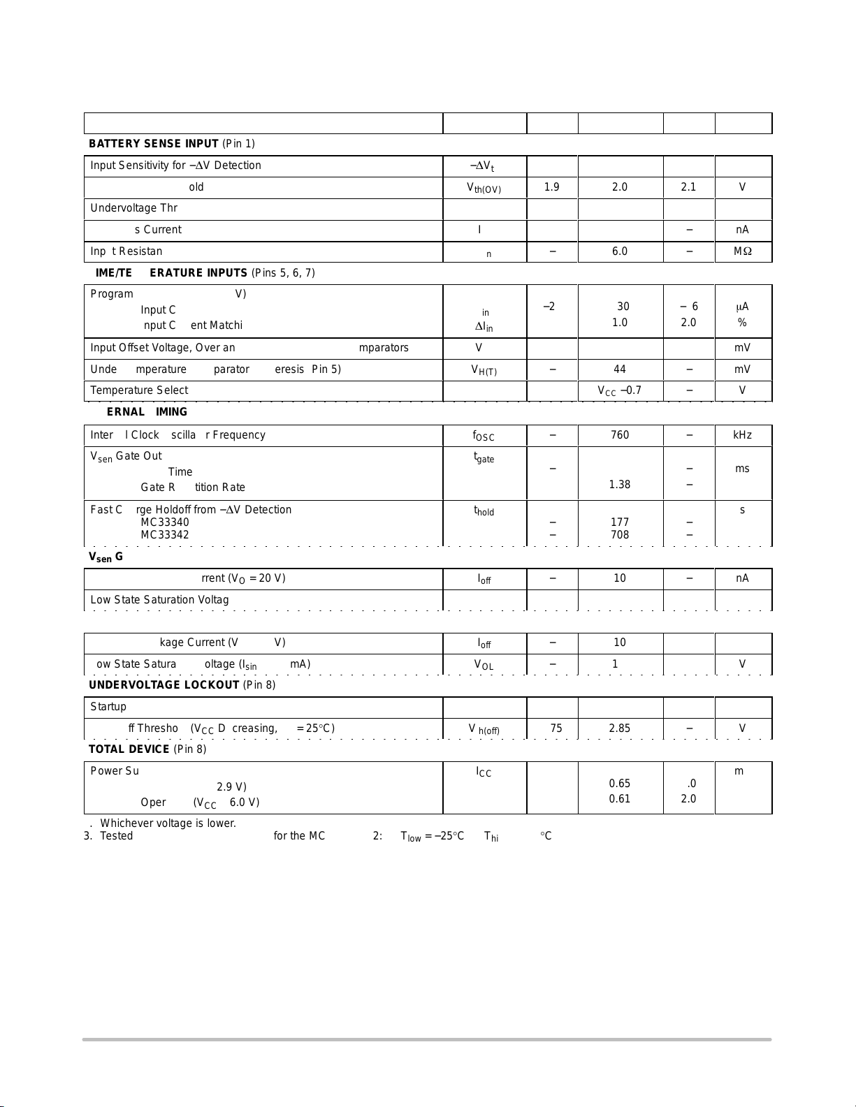
MC33340 has a typical holdoff time of 177 seconds and the
MC33342 has a typical holdoff time of 708 seconds.
• Negative Slope Voltage Detection with 4.0 mV Sensitivity
• Accurate Zero Current Battery Voltage Sensing
• High Noise Immunity with Synchronous VFC/Logic
• Programmable 1 to 4 Hour Fast Charge Time Limit
• Programmable Over/Undertemperature Detection
• Battery Over and Undervoltage Fast Charge Protection
• Power Supply Input Undervoltage Lockout with Hysteresis
• Operating Voltage Range of 3.25 V to 18 V
• 177 seconds Fast Change Holdoff Time (MC33340)
• 708 seconds Fast Change Holdoff Time (MC33342)
• Pb−Free Packages are Available
DC
Input
Regulator
Undervoltage
Counter
Timer
Over
Under
4
Lockout
t1
t2
t3
t/T
Time/
Temp Select
R
Q
S
Internal Bias
V
sen
1
V
sen
Gate
2
3
Fast/
Trickle
This device contains 2,512 active transistors.
Voltage to
Frequency
Converter
Battery
Detect
Ck F/V R
High
Low
−DV Detect
V
sen
Gate
F/T
GND
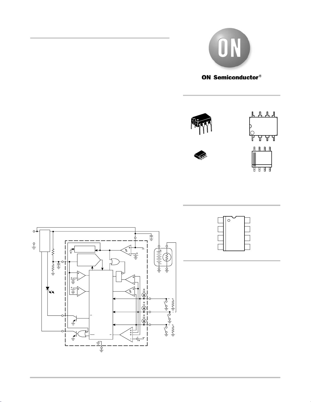
Figure 1. Simplified Block Diagram
Over
Temp
Latch
Temp
Detect
8
V
CC
V
CC
Battery
Pack
t1/T
High
ref
7
t2/T
sen
6
t3/T
Low
ref
5
V
CC
http://onsemi.com
MARKING
DIAGRAMS
8
PDIP−8
P SUFFIX
8
1
8
1
CASE 626
SOIC−8
NB SUFFIX
CASE 751
x = 0 or 2
A = Assembly Location
L = Wafer Lot
Y = Year
W = Work Week
G = Pb−Free Package
MC3334xP
AWL
YYWW
1
8
3334x
ALYWX
G
1
PIN CONNECTIONS
V
Input
sen
V
Gate Output
sen
Fast/Trickle Output
Gnd
1
2
3
4
(Top View)
8V
CC
t1/T
High
7
ref
6
t2/T
sen
5
t3/T
Low
ref
ORDERING INFORMATION
See detailed ordering and shipping information in the package
dimensions section on page 13 of this data sheet.
© Semiconductor Components Industries, LLC, 2005
July, 2005 − Rev. 7
1 Publication Order Number:
MC33340/D

MC33340, MC33342
MAXIMUM RATINGS (Note 1)
Rating Symbol Value Unit
Power Supply Voltage (Pin 8) V
CC
Input Voltage Range
Time/Temperature Select (Pins 5, 6, 7) V
Battery Sense, (Note 2) (Pin 1) V
V
Gate Output (Pin 2)
sen
Voltage
Current
IR(t/T)
IR(sen)
V
O(gate)
I
O(gate)
−1.0 to VCC + 0.6 or −1.0 to 10
Fast/Trickle Output (Pin 3)
Voltage
Current
Thermal Resistance, Junction−to−Air
V
O(F/T)
I
O(F/T)
R
q
JA
P Suffix, DIP Plastic Package, Case 626 100
D Suffix, SO−8 Plastic Package, Case 751 178
Operating Junction Temperature T
Operating Ambient Temperature (Note 3) T
Storage Temperature T
J
A
stg
Maximum ratings are those values beyond which device damage can occur. Maximum ratings applied to the device are individual stress limit
values (not normal operating conditions) and are not valid simultaneously. If these limits are exceeded, device functional operation is not implied,
damage may occur and reliability may be affected.
1. This device series contains ESD protection and exceeds the following tests:
Human Body Model 2000 V per MIL−STD−883, Method 3015 Machine Model Method 400 V
18 V
−1.0 to V
CC
20
50
mA
20
50
mA
°C/W
+150 °C
−25 to +85 °C
−55 to +150 °C
V
V
V
http://onsemi.com
2
MC33340, MC33342
Á
Á
Á
Á
Á
Á
Á
Á
Á
Á
Á
Á
Á
Á
Á
Á
Á
Á
Á
Á
Á
Á
Á
Á
Á
Á
Á
Á
Á
Á
ELECTRICAL CHARACTERISTICS (V
= 6.0 V, for typical values TA = 25°C, for min/max values TA is the operating
CC
ambient temperature range that applies (Note 3), unless otherwise noted.)
Characteristic Symbol Min Typ Max Unit
BATTERY SENSE INPUT (Pin 1)
Input Sensitivity for −DV Detection
Overvoltage Threshold
Undervoltage Threshold
Input Bias Current
Input Resistance
TIME/TEMPERATURE INPUTS (Pins 5, 6, 7)
Programing Inputs (Vin = 1.5 V)
ББББББББББББББББ
Input Current
Input Current Matching
Input Offset Voltage, Over and Under Temperature Comparators
Under Temperature Comparator Hysteresis (Pin 5)
Temperature Select Threshold
INTERNAL TIMING
Internal Clock Oscillator Frequency
V
Gate Output (Pin 2)
sen
ББББББББББББББББ
ББББББББББББББББ
Gate Time
Gate Repetition Rate
Fast Charge Holdoff from −DV Detection
ББББББББББББББББ
V
sen
MC33340
MC33342
GATE OUTPUT (Pin 2)
Off−State Leakage Current (VO = 20 V)
Low State Saturation Voltage (I
= 10 mA)
sink
FAST/TRICKLE OUTPUT (Pin 3)
Off−State Leakage Current (VO = 20 V)
Low State Saturation Voltage (I
= 10 mA)
sink
UNDERVOLTAGE LOCKOUT (Pin 8)
Startup Threshold (VCC Increasing, TA = 25°C)
Turn−Off Threshold (VCC Decreasing, TA = 25°C)
TOTAL DEVICE (Pin 8)
Power Supply Current (Pins 5, 6, 7 Open)
ББББББББББББББББ
Startup (V
Operating (V
CC
CC
= 2.9 V)
= 6.0 V)
2. Whichever voltage is lower.
3. Tested junction temperature range for the MC33340/342: T
= −25°CT
low
−DV
th
V
th(OV)
V
th(UV)
I
IB
R
in
I
in
ÁÁÁ
DI
in
V
IO
V
H(T)
V
th(t/T)
f
OSC
t
gate
ÁÁÁ
ÁÁÁ
t
hold
ÁÁÁ
I
off
V
OL
I
off
V
OL
V
th(on)
V
th(off)
I
CC
ÁÁÁ
high
0.95
Á
Á
Á
Á
2.75
Á
= +85°C
−
1.9
−
−
−24
−
−
−
−
−
−
−
−
−
−
−
−
−
−
−
−
−4.0
2.0
1.0
10
6.0
−30
ÁÁÁ
1.0
5.0
44
VCC −0.7
760
ÁÁÁ
33
1.38
ÁÁÁ
177
ÁÁÁ
708
10
1.2
10
1.0
3.0
2.85
0.65
ÁÁÁ
0.61
−
2.1
1.05
−
−
−36
ÁÁ
2.0
−
−
−
−
ÁÁ
−
−
ÁÁ
−
ÁÁ
−
−
−
−
−
3.25
−
2.0
ÁÁ
2.0
mV
V
mV
nA
MW
mA
Á
%
mV
mV
V
kHz
Á
ms
s
Á
s
Á
nA
V
nA
V
V
V
mA
Á
http://onsemi.com
3
MC33340, MC33342
)
t
sen
V
2.10
VCC = 6.0 V
2.00
1.90
1.02
1.00
, OVER/UNDERVOLTAGE THRESHOLDS (V
0.98
th
V
−50 −25 0 25 50 75 100 125
TA, AMBIENT TEMPERATURE (°C)
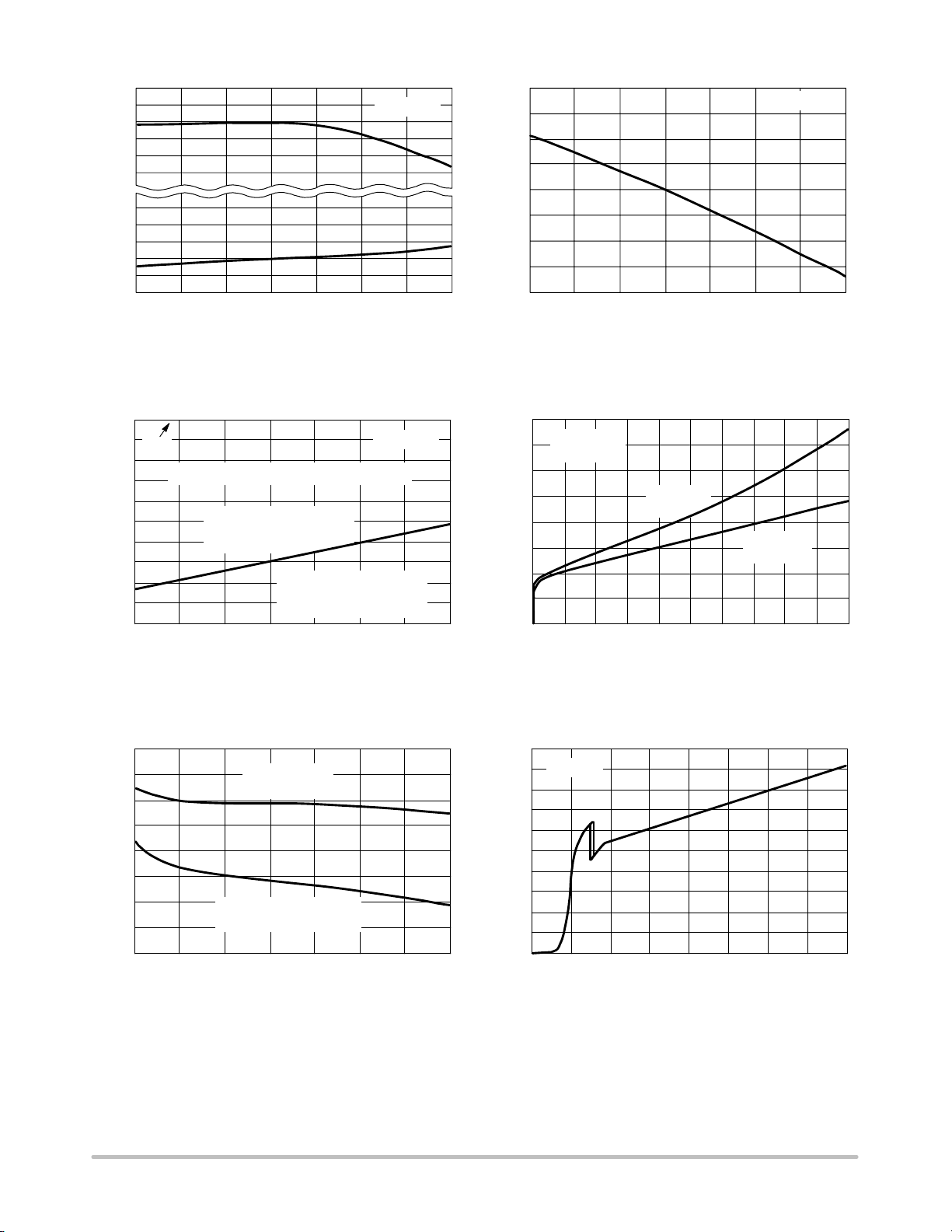
Figure 2. Battery Sense Input Thresholds
versus Temperature
0
V
CC
−0.2
−0.4
−0.6
−0.8
−1.0
, TEMPERATURE SELECT THRESHOLD VOLTAGE (
Threshold voltage is measured with respect to VCC.
Time mode is selected if any of
the three inputs are above the
threshold.
Temperature mode is selected
when all three inputs are below
the threshold.
−50 −25 0 25 50 75 100 125
TA, AMBIENT TEMPERATURE (°C)
VCC = 6.0 V
Figure 4. Temperature Select Threshold Voltage
th(t/T)
V
versus Temperature
16
8.0
0
−8.0
, OSCILLATOR FREQUENCY CHANGE (%Δ
−16
OSC
f
−50 −25 0 25 50 75 100 125
TA, AMBIENT TEMPERATURE (°C)
VCC = 6.0 V
Figure 3. Oscillator Frequency
versus Temperature
3.2
VCC = 6.0 V
TA = 25°C
2.4
V
Gate
sen
Pin 2
1.6
Fast/Trickle
Pin 3
0.8
, SINK SATURATION VOLTAGE (V)
OL
V
0
0 8.0 16 24 32 40
I
, SINK SATURATION (mA)
sink
Figure 5. Saturation Voltage versus Sink Curren
V
Gate and Fast/Trickle Outputs
3.1
Startup Threshold
3.0
2.9
, SUPPLY VOLTAGE (V)
2.8
CC
V
2.7
−50
−25 0 25 50 75 100 125
(VCC Increasing)
Minimum Operating Threshold
(VCC Decreasing)
TA, AMBIENT TEMPERATURE (°C)
Figure 6. Undervoltage Lockout Thresholds
versus Temperature
1.0
TA = 25°C
0.8
0.6
0.4
, SUPPLY CURRENT (mA)
CC
0.2
I
0
0 4.0 8.0 12 16
VCC, SUPPLY VOLTAGE (V)
Figure 7. Supply Current
versus Supply Voltage
http://onsemi.com
4
MC33340, MC33342
INTRODUCTION
Nickel Cadmium and Nickel Metal Hydride batteries
require precise charge termination control to maximize cell
capacity and operating time while preventing overcharging.
Overcharging can result in a reduction of battery life as well
as physical harm to the end user. Since most portable
applications require the batteries to be charged rapidly, a
primary and u sually a s econdary o r r edundant char ge s ensi ng
technique is employed into the charging system. It is also
desirable to disable rapid charging if the battery voltage or
temperature is either t oo h i gh or too low. In order t o a ddress
these issues , an economical a nd flexi ble fa st char ge c ontroller
was developed.
The MC33340/342 contains many of the building blocks
and protection features that are employed in modern high
performance battery charger controllers that are specifically
designed for Nickel Cadmium and Nickel Metal Hydride
batteries. The device is designed to interface with either
primary or secondary side regulators for easy implementation
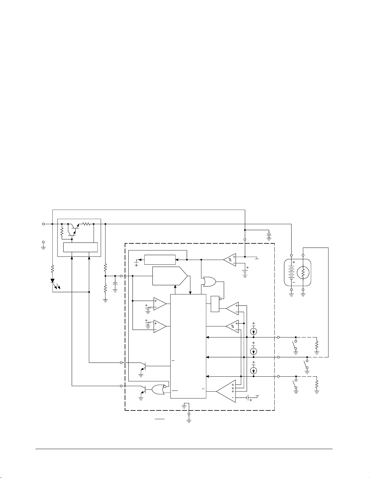
of a complet e charging system. A represent ative block d iagram
in a typical charging application is shown in Figure 8.
The battery voltage is monitored by the V
input that
sen
internally connects to a voltage to frequency converter and
Regulator
counter for d etection o f a n egati ve slope in bat tery v ol tage. A
timer with three programming inputs is available to provide
backup charge termi nation. A lternati vely , these input s ca n be
used to monitor the battery pack temperature and to set the
over and undertemperature limits also for backup charge
termination.
Two active low open collector outputs are provided to
interface this controller with the external charging circuit.
The first output furnishes a gating pulse that momentarily
interrupts the charge c urrent. This a llows a n a ccurate m ethod
of sampling the battery voltage by eliminating voltage drops
that are associated with high charge currents and wiring
resistances. Also, any noise voltages generated by the
charging circuitry are eliminated. The second output is
designed to switch the charging source between fast and
trickle modes based upon the results of voltage, time, or
temperature. These outputs normally connect directly to a
linear or switching regulator control circuit in non−isolated
primary or secondary side applications. Both outputs can be
used to drive optoisolators in primary side applications that
require galvanic isolation. Figure 9 shows the typical charge
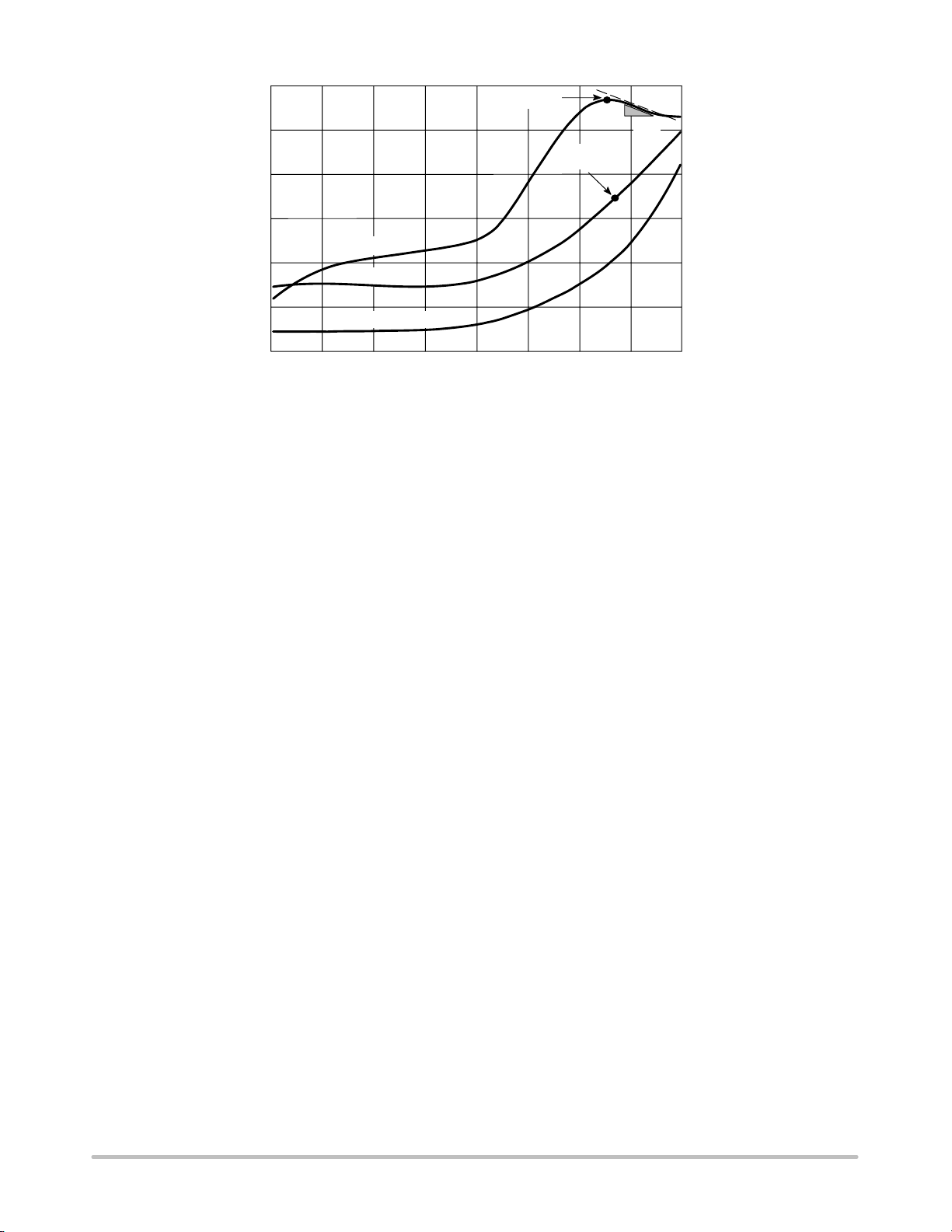
characteristics for NiCd and NiMh batteries.
DC
Input
Charge
Status
Reg Control
R2
R1
MC33340 or MC33342
Undervoltage
Under
4
Over
t/T
Lockout
Q
t1
t2
t3
Time/
Temp
Select
V
sen
V
sen
Gate
Fast/
Trickle
1
2
3
2.0 V
1.0 V
R2 + R1
Internal Bias
Voltage to
Frequency
Converter
Battery
Detect
V
Batt
ǒ
–1
V
sen
Ck F/V R
High
Low
−DV Detect
Counter
Timer
V
sen
Gate
F/T
Gnd
Ǔ
Figure 8. Typical Battery Charging Application
R
S
Over
Temp
Latch
Temp
Detect
V
8
CC
V
CC
0.7 V
2.9 V
V
30 mA
30 mA
30 mA
CC
t1/T
7
t2/T
6
t3/T
5
ref
sen
ref
Battery
High
Low
Pack
T
SW1
SW3
R
SW2
NTC
R3
R4
http://onsemi.com
5
MC33340, MC33342
1.6
1.5
1.4
1.3
CELL VOLTAGE (V)
1.2
1.1
1.0
0 40 80 120 160
Figure 9. Typical Charge Characteristics for NiCd and NiMh Batteries
Voltage
Temperature
Relative Pressure
CHARGE INPUT PERCENT OF CAPACITY
OPERATING DESCRIPTION
The MC33340/342 starts up in the fast charge mode when
power is applied to VCC. A change to the trickle mode can
occur as a result of three possible conditions. The first is if
the V
input voltage is above 2.0 V or below 1.0 V. Above
sen
2.0 V indicates that the battery pack is open or disconnected,
while below 1.0 V indicates the possibility of a shorted or
defective cell. The second condition is when the
MC33340/342 detects a fully charged battery by measuring
a negative slope in battery voltage. The MC33340/342
recognize a negative voltage slope after the preset holdoff
time (t
) has elapsed during a fast charge cycle. This
hold
indicates that the battery pack is fully charged. The third
condition is either due to the battery pack being out of a
programmed temperature range, or that the preset timer
period has been exceeded.
There are three conditions that will cause the controller to
return from trickle to fast charge mode. The first is if the V
sen
input voltage moved to within the 1.0 to 2.0 V range from
initially being either too high or too low . The second is if the
battery pack temperature moved to within the programmed
temperature range, but only from initially being too cold.
Third is by cycling VCC off and then back on causing the
internal logic to reset. A concise description of the major
circuit blocks is given below.
Negative Slope Voltage Detection
A representative block diagram of the negative slope
voltage detector is shown in Figure 10. It includes a
Synchronous Voltage to Frequency Converter, a Sample
Timer, and a Ratchet Counter. The V
pin is the input for
sen
the Voltage to Frequency Converter (VFC), and it connects
to the rechargeable battery pack terminals through a
dt
−DV
70
60
50
40
30
CELL TEMPERATURE ( C)°
20
10
V
max
dV
T
max
resistive voltage divider. The input has an impedance of
approximately 6.0 MW and a maximum voltage range of
−1.0 V to VCC + 0.6 V or 0 V to 10 V, whichever is lower.
The 10 V upper limit is set by an internal zener clamp that
provides protection in the event of an electrostatic discharge.
The VFC is a charge−balanced synchronous type which
generates output pulses at a rate of FV = V
(24 kHz).
sen
The Sample Timer circuit provides a 95 kHz system clock
signal (SCK) to the VFC. This signal synchronizes the F
output to the other Sample Timer outputs used within the
detector. At 1.38 second intervals the V
Gate output goes
sen
low for a 33 ms period. This output is used to momentarily
interrupt the external charging power source so that a precise
voltage measurement can be taken. As the V
Gate goes
sen
low, the internal Preset control line is driven high for 11 ms.
During this time, the battery voltage at the V
input is
sen
allowed to stabilize and the previous FV count is preloaded.
At the Preset high−to−low transition, the Convert line goes
high for 22 ms. This gates the F
pulses into the ratchet
V
counter for a comparison to the preloaded count. Since the
Convert time is derived from the same clock that controls the
VFC, the number of FV pulses is independent of the clock
frequency. If the new sample has more counts than were
preloaded, it becomes the new peak count and the cycle is
repeated 1.38 seconds later. If the new sample has two fewer
counts, a less than peak voltage event has occurred, and a
register is initialized. If two successive less than peak
voltage events occur, the −DV ‘AND’ gate output goes high
and the Fast/Trickle output is latched in a low state,
signifying that the battery pack has reached full charge
status.
V
http://onsemi.com
6
 Loading...