

Page 1
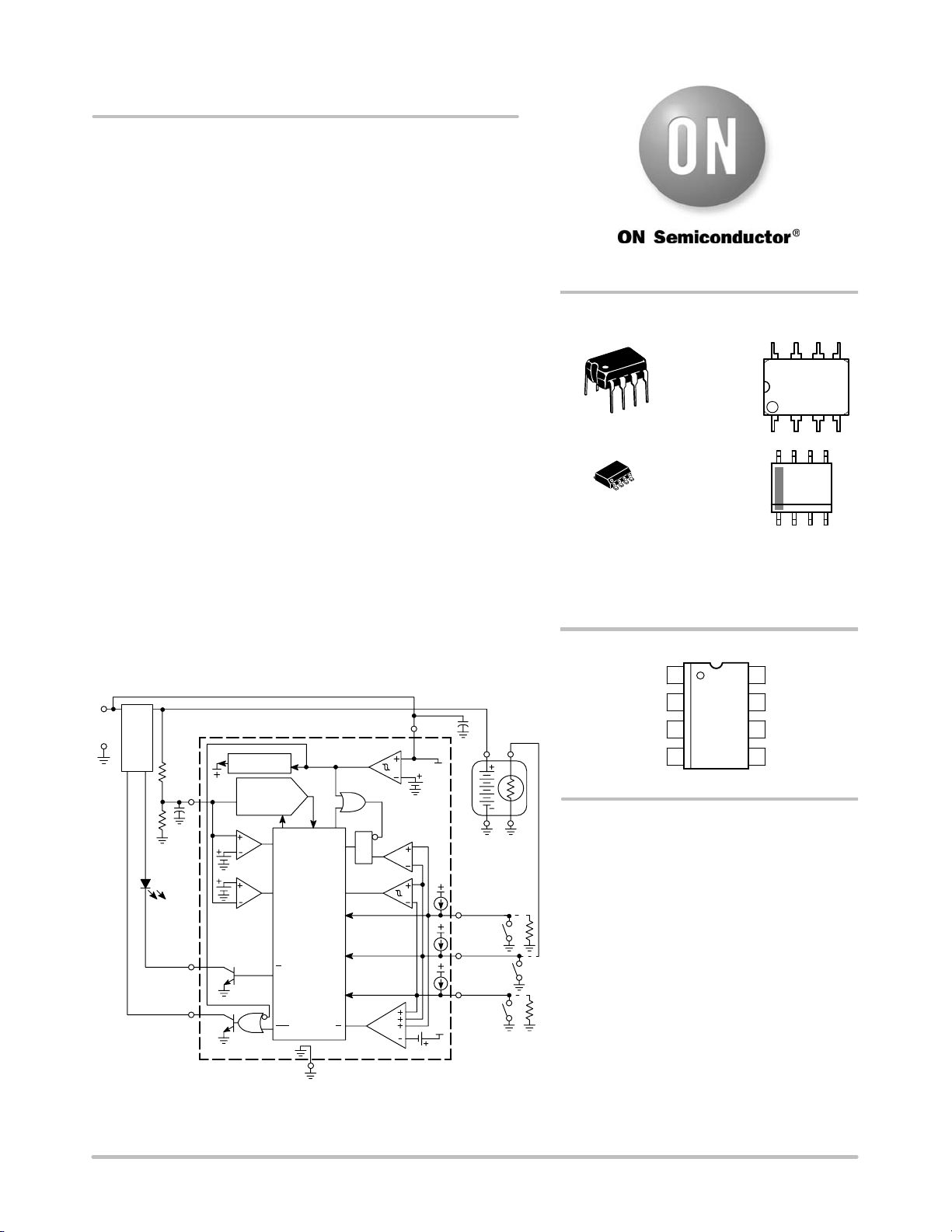
MC33340, MC33342
Battery Fast Charge
Controllers
The MC33340 and MC33342 are monolithic control IC’s that are
specifically designed as fast charge controllers for Nickel Cadmium
(NiCd) and Nickel Metal Hydride (NiMH) batteries. These devices
feature negative slope voltage detection as the primary means for fast
charge termination. Accurate detection is ensured by an output that
momentarily interrupts the charge current for precise voltage
sampling. An additional secondary backup termination method can
be selected that consists of either a programmable time or temperature
limit. Protective features include battery over and undervoltage
detection, latched over temperature detection, and power supply input
undervoltage lockout with hysteresis. Fast charge holdoff time is the
only difference between the MC33340 and the MC33342. The
MC33340 has a typical holdoff time of 177 seconds and the
MC33342 has a typical holdoff time of 708 seconds.
• Negative Slope Voltage Detection with 4.0 mV Sensitivity
• Accurate Zero Current Battery Voltage Sensing
• High Noise Immunity with Synchronous VFC/Logic
• Programmable 1 to 4 Hour Fast Charge Time Limit
• Programmable Over/Undertemperature Detection
• Battery Over and Undervoltage Fast Charge Protection
• Power Supply Input Undervoltage Lockout with Hysteresis
• Operating Voltage Range of 3.25 V to 18 V
• 177 seconds Fast Change Holdoff Time (MC33340)
• 708 seconds Fast Change Holdoff Time (MC33342)
• Pb−Free Packages are Available
DC
Input
Regulator
Undervoltage
Counter
Timer
Over
Under
4
Lockout
t1
t2
t3
t/T
Time/
Temp Select
R
Q
S
Internal Bias
V
sen
1
V
sen
Gate
2
3
Fast/
Trickle
This device contains 2,512 active transistors.
Voltage to
Frequency
Converter
Battery
Detect
Ck F/V R
High
Low
−DV Detect
V
sen
Gate
F/T
GND
Figure 1. Simplified Block Diagram
Over
Temp
Latch
Temp
Detect
8
V
CC
V
CC
Battery
Pack
t1/T
High
ref
7
t2/T
sen
6
t3/T
Low
ref
5
V
CC
http://onsemi.com
MARKING
DIAGRAMS
8
PDIP−8
P SUFFIX
8
1
8
1
CASE 626
SOIC−8
NB SUFFIX
CASE 751
x = 0 or 2
A = Assembly Location
L = Wafer Lot
Y = Year
W = Work Week
G = Pb−Free Package
MC3334xP
AWL
YYWW
1
8
3334x
ALYWX
G
1
PIN CONNECTIONS
V
Input
sen
V
Gate Output
sen
Fast/Trickle Output
Gnd
1
2
3
4
(Top View)
8V
CC
t1/T
High
7
ref
6
t2/T
sen
5
t3/T
Low
ref
ORDERING INFORMATION
See detailed ordering and shipping information in the package
dimensions section on page 13 of this data sheet.
© Semiconductor Components Industries, LLC, 2005
July, 2005 − Rev. 7
1 Publication Order Number:
MC33340/D
Page 2
MC33340, MC33342
MAXIMUM RATINGS (Note 1)
Rating Symbol Value Unit
Power Supply Voltage (Pin 8) V
CC
Input Voltage Range
Time/Temperature Select (Pins 5, 6, 7) V
Battery Sense, (Note 2) (Pin 1) V
V
Gate Output (Pin 2)
sen
Voltage
Current
IR(t/T)
IR(sen)
V
O(gate)
I
O(gate)
−1.0 to VCC + 0.6 or −1.0 to 10
Fast/Trickle Output (Pin 3)
Voltage
Current
Thermal Resistance, Junction−to−Air
V
O(F/T)
I
O(F/T)
R
q
JA
P Suffix, DIP Plastic Package, Case 626 100
D Suffix, SO−8 Plastic Package, Case 751 178
Operating Junction Temperature T
Operating Ambient Temperature (Note 3) T
Storage Temperature T
J
A
stg
Maximum ratings are those values beyond which device damage can occur. Maximum ratings applied to the device are individual stress limit
values (not normal operating conditions) and are not valid simultaneously. If these limits are exceeded, device functional operation is not implied,
damage may occur and reliability may be affected.
1. This device series contains ESD protection and exceeds the following tests:
Human Body Model 2000 V per MIL−STD−883, Method 3015 Machine Model Method 400 V
18 V
−1.0 to V
CC
20
50
mA
20
50
mA
°C/W
+150 °C
−25 to +85 °C
−55 to +150 °C
V
V
V
http://onsemi.com
2
Page 3
MC33340, MC33342
Á
Á
Á
Á
Á
Á
Á
Á
Á
Á
Á
Á
Á
Á
Á
Á
Á
Á
Á
Á
Á
Á
Á
Á
Á
Á
Á
Á
Á
Á
ELECTRICAL CHARACTERISTICS (V
= 6.0 V, for typical values TA = 25°C, for min/max values TA is the operating
CC
ambient temperature range that applies (Note 3), unless otherwise noted.)
Characteristic Symbol Min Typ Max Unit
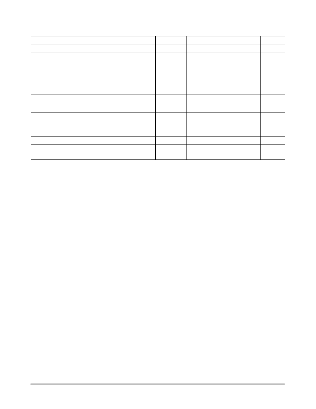
BATTERY SENSE INPUT (Pin 1)
Input Sensitivity for −DV Detection
Overvoltage Threshold
Undervoltage Threshold
Input Bias Current
Input Resistance
TIME/TEMPERATURE INPUTS (Pins 5, 6, 7)
Programing Inputs (Vin = 1.5 V)
ББББББББББББББББ
Input Current
Input Current Matching
Input Offset Voltage, Over and Under Temperature Comparators
Under Temperature Comparator Hysteresis (Pin 5)
Temperature Select Threshold
INTERNAL TIMING
Internal Clock Oscillator Frequency
V
Gate Output (Pin 2)
sen
ББББББББББББББББ
ББББББББББББББББ
Gate Time
Gate Repetition Rate
Fast Charge Holdoff from −DV Detection
ББББББББББББББББ
V
sen
MC33340
MC33342
GATE OUTPUT (Pin 2)
Off−State Leakage Current (VO = 20 V)
Low State Saturation Voltage (I
= 10 mA)
sink
FAST/TRICKLE OUTPUT (Pin 3)
Off−State Leakage Current (VO = 20 V)
Low State Saturation Voltage (I
= 10 mA)
sink
UNDERVOLTAGE LOCKOUT (Pin 8)
Startup Threshold (VCC Increasing, TA = 25°C)
Turn−Off Threshold (VCC Decreasing, TA = 25°C)
TOTAL DEVICE (Pin 8)
Power Supply Current (Pins 5, 6, 7 Open)
ББББББББББББББББ
Startup (V
Operating (V
CC
CC
= 2.9 V)
= 6.0 V)
2. Whichever voltage is lower.
3. Tested junction temperature range for the MC33340/342: T
= −25°CT
low
−DV
th
V
th(OV)
V
th(UV)
I
IB
R
in
I
in
ÁÁÁ
DI
in
V
IO
V
H(T)
V
th(t/T)
f
OSC
t
gate
ÁÁÁ
ÁÁÁ
t
hold
ÁÁÁ
I
off
V
OL
I
off
V
OL
V
th(on)
V
th(off)
I
CC
ÁÁÁ
high
0.95
Á
Á
Á
Á
2.75
Á
= +85°C
−
1.9
−
−
−24
−
−
−
−
−
−
−
−
−
−
−
−
−
−
−
−
−4.0
2.0
1.0
10
6.0
−30
ÁÁÁ
1.0
5.0
44
VCC −0.7
760
ÁÁÁ
33
1.38
ÁÁÁ
177
ÁÁÁ
708
10
1.2
10
1.0
3.0
2.85
0.65
ÁÁÁ
0.61
−
2.1
1.05
−
−
−36
ÁÁ
2.0
−
−
−
−
ÁÁ
−
−
ÁÁ
−
ÁÁ
−
−
−
−
−
3.25
−
2.0
ÁÁ
2.0
mV
V
mV
nA
MW
mA
Á
%
mV
mV
V
kHz
Á
ms
s
Á
s
Á
nA
V
nA
V
V
V
mA
Á
http://onsemi.com
3
Page 4
MC33340, MC33342
)
t
sen
V
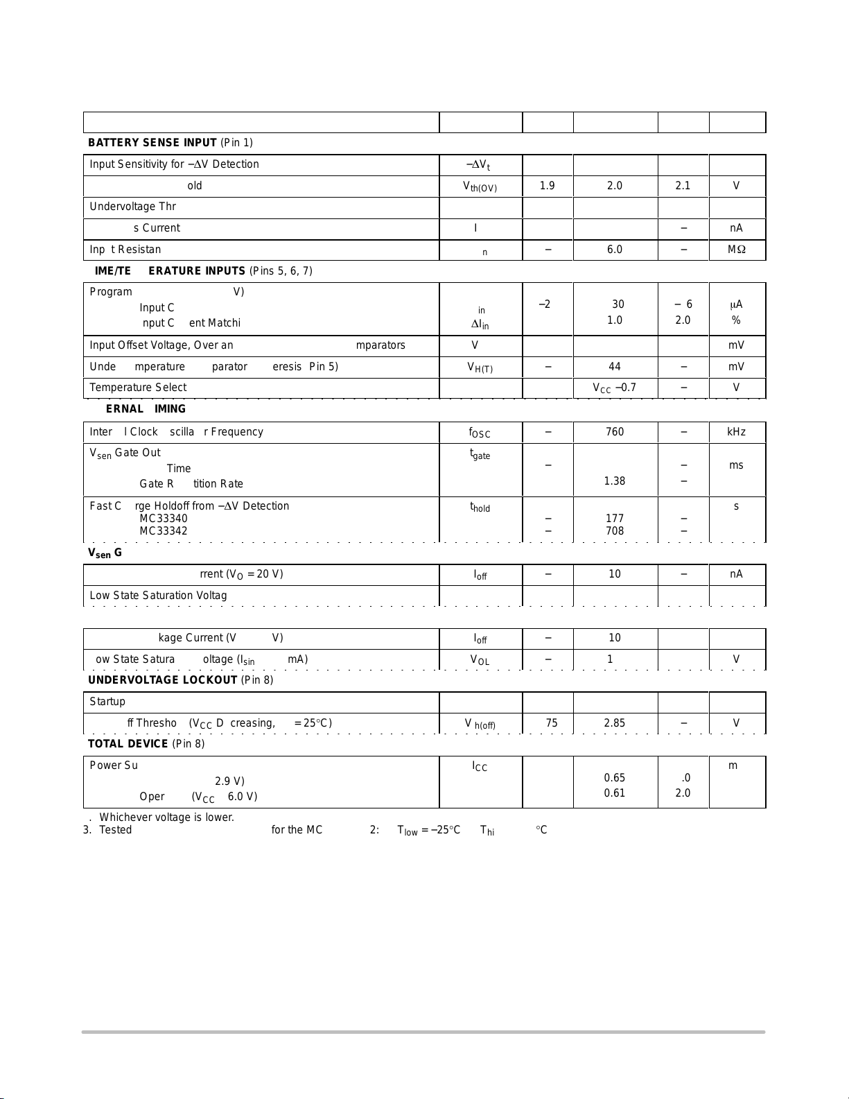
2.10
VCC = 6.0 V
2.00
1.90
1.02
1.00
, OVER/UNDERVOLTAGE THRESHOLDS (V
0.98
th
V
−50 −25 0 25 50 75 100 125
TA, AMBIENT TEMPERATURE (°C)
Figure 2. Battery Sense Input Thresholds
versus Temperature
0
V
CC
−0.2
−0.4
−0.6
−0.8
−1.0
, TEMPERATURE SELECT THRESHOLD VOLTAGE (
Threshold voltage is measured with respect to VCC.
Time mode is selected if any of
the three inputs are above the
threshold.
Temperature mode is selected
when all three inputs are below
the threshold.
−50 −25 0 25 50 75 100 125
TA, AMBIENT TEMPERATURE (°C)
VCC = 6.0 V
Figure 4. Temperature Select Threshold Voltage
th(t/T)
V
versus Temperature
16
8.0
0
−8.0
, OSCILLATOR FREQUENCY CHANGE (%Δ
−16
OSC
f
−50 −25 0 25 50 75 100 125
TA, AMBIENT TEMPERATURE (°C)
VCC = 6.0 V
Figure 3. Oscillator Frequency
versus Temperature
3.2
VCC = 6.0 V
TA = 25°C
2.4
V
Gate
sen
Pin 2
1.6
Fast/Trickle
Pin 3
0.8
, SINK SATURATION VOLTAGE (V)
OL
V
0
0 8.0 16 24 32 40
I
, SINK SATURATION (mA)
sink
Figure 5. Saturation Voltage versus Sink Curren
V
Gate and Fast/Trickle Outputs
3.1
Startup Threshold
3.0
2.9
, SUPPLY VOLTAGE (V)
2.8
CC
V
2.7
−50
−25 0 25 50 75 100 125
(VCC Increasing)
Minimum Operating Threshold
(VCC Decreasing)
TA, AMBIENT TEMPERATURE (°C)
Figure 6. Undervoltage Lockout Thresholds
versus Temperature
1.0
TA = 25°C
0.8
0.6
0.4
, SUPPLY CURRENT (mA)
CC
0.2
I
0
0 4.0 8.0 12 16
VCC, SUPPLY VOLTAGE (V)
Figure 7. Supply Current
versus Supply Voltage
http://onsemi.com
4
Page 5
MC33340, MC33342
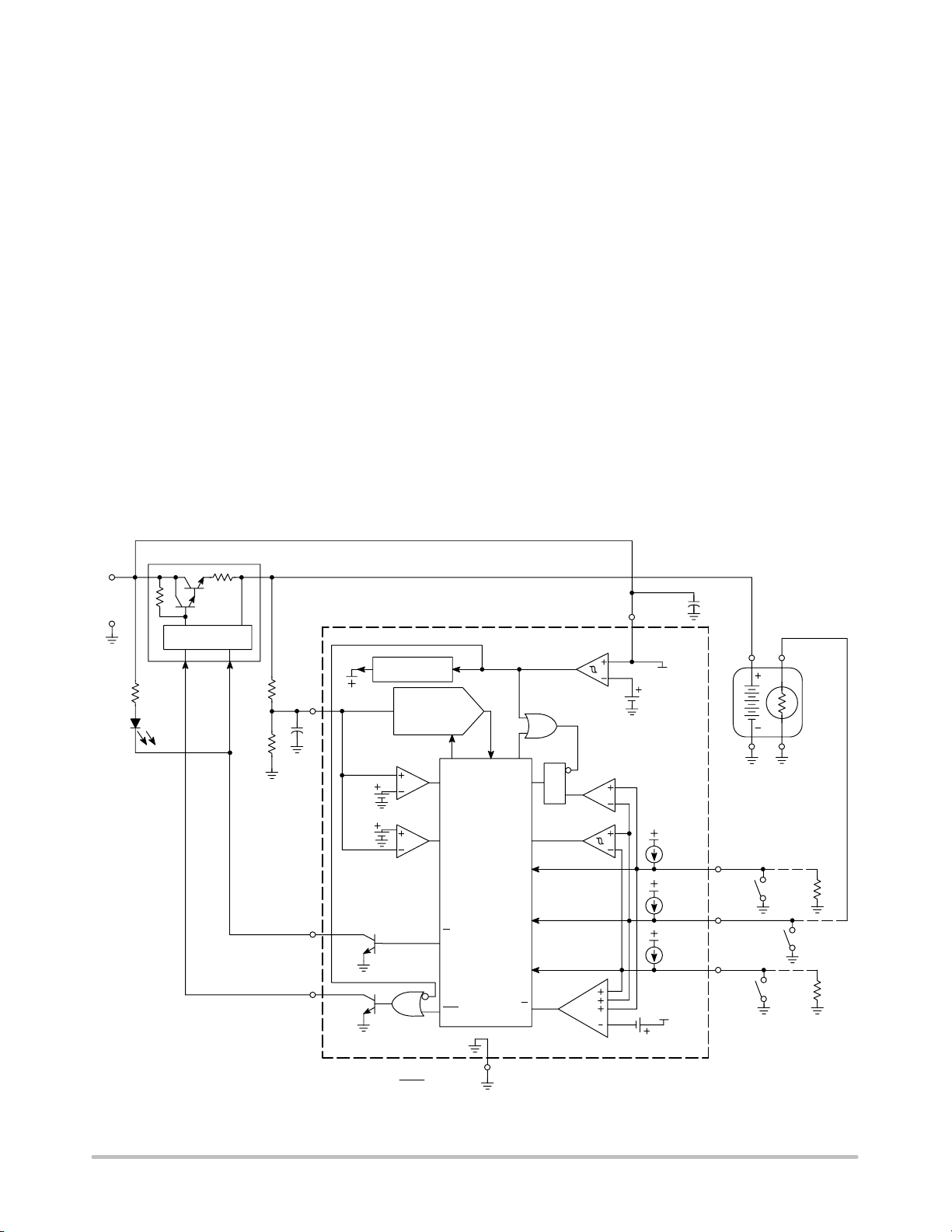
INTRODUCTION
Nickel Cadmium and Nickel Metal Hydride batteries
require precise charge termination control to maximize cell
capacity and operating time while preventing overcharging.
Overcharging can result in a reduction of battery life as well
as physical harm to the end user. Since most portable
applications require the batteries to be charged rapidly, a
primary and u sually a s econdary o r r edundant char ge s ensi ng
technique is employed into the charging system. It is also
desirable to disable rapid charging if the battery voltage or
temperature is either t oo h i gh or too low. In order t o a ddress
these issues , an economical a nd flexi ble fa st char ge c ontroller
was developed.
The MC33340/342 contains many of the building blocks
and protection features that are employed in modern high
performance battery charger controllers that are specifically
designed for Nickel Cadmium and Nickel Metal Hydride
batteries. The device is designed to interface with either
primary or secondary side regulators for easy implementation
of a complet e charging system. A represent ative block d iagram
in a typical charging application is shown in Figure 8.
The battery voltage is monitored by the V
input that
sen
internally connects to a voltage to frequency converter and
Regulator
counter for d etection o f a n egati ve slope in bat tery v ol tage. A
timer with three programming inputs is available to provide
backup charge termi nation. A lternati vely , these input s ca n be
used to monitor the battery pack temperature and to set the
over and undertemperature limits also for backup charge
termination.
Two active low open collector outputs are provided to
interface this controller with the external charging circuit.
The first output furnishes a gating pulse that momentarily
interrupts the charge c urrent. This a llows a n a ccurate m ethod
of sampling the battery voltage by eliminating voltage drops
that are associated with high charge currents and wiring
resistances. Also, any noise voltages generated by the
charging circuitry are eliminated. The second output is
designed to switch the charging source between fast and
trickle modes based upon the results of voltage, time, or
temperature. These outputs normally connect directly to a
linear or switching regulator control circuit in non−isolated
primary or secondary side applications. Both outputs can be
used to drive optoisolators in primary side applications that
require galvanic isolation. Figure 9 shows the typical charge
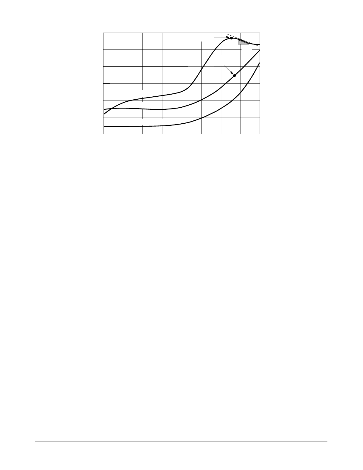
characteristics for NiCd and NiMh batteries.
DC
Input
Charge
Status
Reg Control
R2
R1
MC33340 or MC33342
Undervoltage
Under
4
Over
t/T
Lockout
Q
t1
t2
t3
Time/
Temp
Select
V
sen
V
sen
Gate
Fast/
Trickle
1
2
3
2.0 V
1.0 V
R2 + R1
Internal Bias
Voltage to
Frequency
Converter
Battery
Detect
V
Batt
ǒ
–1
V
sen
Ck F/V R
High
Low
−DV Detect
Counter
Timer
V
sen
Gate
F/T
Gnd
Ǔ
Figure 8. Typical Battery Charging Application
R
S
Over
Temp
Latch
Temp
Detect
V
8
CC
V
CC
0.7 V
2.9 V
V
30 mA
30 mA
30 mA
CC
t1/T
7
t2/T
6
t3/T
5
ref
sen
ref
Battery
High
Low
Pack
T
SW1
SW3
R
SW2
NTC
R3
R4
http://onsemi.com
5
Page 6
MC33340, MC33342
1.6
1.5
1.4
1.3
CELL VOLTAGE (V)
1.2
1.1
1.0
0 40 80 120 160
Figure 9. Typical Charge Characteristics for NiCd and NiMh Batteries
Voltage
Temperature
Relative Pressure
CHARGE INPUT PERCENT OF CAPACITY
OPERATING DESCRIPTION
The MC33340/342 starts up in the fast charge mode when
power is applied to VCC. A change to the trickle mode can
occur as a result of three possible conditions. The first is if
the V
input voltage is above 2.0 V or below 1.0 V. Above
sen
2.0 V indicates that the battery pack is open or disconnected,
while below 1.0 V indicates the possibility of a shorted or
defective cell. The second condition is when the
MC33340/342 detects a fully charged battery by measuring
a negative slope in battery voltage. The MC33340/342
recognize a negative voltage slope after the preset holdoff
time (t
) has elapsed during a fast charge cycle. This
hold
indicates that the battery pack is fully charged. The third
condition is either due to the battery pack being out of a
programmed temperature range, or that the preset timer
period has been exceeded.
There are three conditions that will cause the controller to
return from trickle to fast charge mode. The first is if the V
sen
input voltage moved to within the 1.0 to 2.0 V range from
initially being either too high or too low . The second is if the
battery pack temperature moved to within the programmed
temperature range, but only from initially being too cold.
Third is by cycling VCC off and then back on causing the
internal logic to reset. A concise description of the major
circuit blocks is given below.
Negative Slope Voltage Detection
A representative block diagram of the negative slope
voltage detector is shown in Figure 10. It includes a
Synchronous Voltage to Frequency Converter, a Sample
Timer, and a Ratchet Counter. The V
pin is the input for
sen
the Voltage to Frequency Converter (VFC), and it connects
to the rechargeable battery pack terminals through a
dt
−DV
70
60
50
40
30
CELL TEMPERATURE ( C)°
20
10
V
max
dV
T
max
resistive voltage divider. The input has an impedance of
approximately 6.0 MW and a maximum voltage range of
−1.0 V to VCC + 0.6 V or 0 V to 10 V, whichever is lower.
The 10 V upper limit is set by an internal zener clamp that
provides protection in the event of an electrostatic discharge.
The VFC is a charge−balanced synchronous type which
generates output pulses at a rate of FV = V
(24 kHz).
sen
The Sample Timer circuit provides a 95 kHz system clock
signal (SCK) to the VFC. This signal synchronizes the F
output to the other Sample Timer outputs used within the
detector. At 1.38 second intervals the V
Gate output goes
sen
low for a 33 ms period. This output is used to momentarily
interrupt the external charging power source so that a precise
voltage measurement can be taken. As the V
Gate goes
sen
low, the internal Preset control line is driven high for 11 ms.
During this time, the battery voltage at the V
input is
sen
allowed to stabilize and the previous FV count is preloaded.
At the Preset high−to−low transition, the Convert line goes
high for 22 ms. This gates the F
pulses into the ratchet
V
counter for a comparison to the preloaded count. Since the
Convert time is derived from the same clock that controls the
VFC, the number of FV pulses is independent of the clock
frequency. If the new sample has more counts than were
preloaded, it becomes the new peak count and the cycle is
repeated 1.38 seconds later. If the new sample has two fewer
counts, a less than peak voltage event has occurred, and a
register is initialized. If two successive less than peak
voltage events occur, the −DV ‘AND’ gate output goes high
and the Fast/Trickle output is latched in a low state,
signifying that the battery pack has reached full charge
status.
V
http://onsemi.com
6
Page 7

MC33340, MC33342
Negative slope voltage detection starts after 60 ms have
elapsed in the fast charge mode. This does not affect the
Fast/Trickle output until the holdoff time (t
) has elapsed
hold
during the fast charge mode. Two scenarios then exist.
Trickle mode holdoff is implemented to ignore any initial
drop in voltage that may occur when charging batteries that
have been stored for an extended time period. If the negative
slope voltage detector senses that initial drop during the
holdoff time, and the input voltage rises as the battery
charges, the Fast/Trickle output will remain open. However,
if the negative slope voltage detector senses a negative drop
FV = V
(24 kHz)
V
sen
Input
Synchronous
Voltage to
Frequency
Converter
SCK
95 kHz
sen
Ck
Convert
Sample
Timer
in voltage during the holdoff time and the input voltage
never rises above that last detected level, the Fast/Trickle
output will latch into a low state. The negative slope voltage
detector has a maximum resolution of 2.0 V divided by
1023 mV, or 1.955 mV per count with an uncertainty of
±1.0 count. This yields a detection range of 1.955 mV to
5.865 mV. In order to obtain maximum sensing accuracy,
the R2/R1 voltage divider must be adjusted so that the V
input voltage is slightly less than 2.0 V when the battery pack
is fully charged. Voltage variations due to temperature and
cell manufacturing must be considered.
Preset
Rachet
Counter
Trickle Mode
Holdoff
−DV
V
Gate
sen
Battery Detect
Over Under
Temperature
UVLOHighLow
Logic
Charge
Timer
sen
F/T
V
Gate
sen
Preset
11 ms
Convert
22 ms
Rachet Counter Convert
0 to 1023 FV Pulses
Figure 10. Negative Slope Voltage Detector
Fast Charge Timer
A programmable backup charge timer is available for fast
charge termination. The timer is activated by the Time/Temp
Select comparator, and is programmed from the t1/T
High, t2/T
, and t3/T
sen
Low inputs. If one or more of these
ref
ref
inputs is allowed to go above VCC − 0.7 V or is left open, the
comparator output will switch high, indicating that the timer
feature is desired. The three inputs allow one of seven
possible fast charge time limits to be selected. The
programmable time limits, rounded to the nearest whole
minute, are shown in Table 1.
Over/Under Temperature Detection
A backup over/under temperature detector is available
and can be used in place of the timer for fast charge
termination. The timer is disabled by the Time/Temp Select
comparator when each of the three programming inputs are
held below VCC − 0.7 V.
1.38 s
Temperature sensing is accomplished by placing a
negative temperature coefficient (NTC) thermistor in
thermal contact with the battery pack. The thermistor
connects to the t2/T
input which has a 30 mA current
sen
source pull−up for developing a temperature dependent
voltage. The temperature limits are set by a resistor that
connects from the t1/T
High and the t3/T
ref
Low inputs to
ref
ground. Since all three inputs contain matched 30 mA
current source pull−ups, the required programming resistor
values are identical to that of the thermistor at the desired
over and under trip temperature. The temperature window
detector is composed of two comparators with a common
input that connects to the t2/T
sen
input.
The lower comparator senses the presence of an under
temperature condition. When the lower temperature limit is
exceeded, the charger is switched to the trickle mode. The
comparator has 44 mV of hysteresis to prevent erratic
http://onsemi.com
7
Page 8
MC33340, MC33342
switching between the fast and trickle modes as the lower
temperature limit is crossed. The amount of temperature rise
to overcome the hysteresis is determined by the thermistor’s
rate of resistance change or sensitivity at the under
temperature trip point. The required resistance change is:
DR(T
Low
³ T
High
) +
H(T)
I
in
+
44 mV
30 mA
+ 1.46 k
V
The resistance change approximates a thermal hysteresis
of 2°C with a 10 kW thermistor operating at 0°C. The under
temperature fast charge inhibit feature can be disabled by
biasing the t3/T
that present at t2/T
Low input to a voltage that is greater than
ref
, and less than VCC − 0.7 V. Under
sen
extremely cold conditions, it is possible that the thermistor
resistance can become t oo h igh, a llowing t he t2/T
sen
input
to go above VCC − 0.7 V, and activate the timer. This
condition can b e p revented b y p lacing a resistor i n parallel
with the thermistor. Note that the time/temperature
threshold of VCC − 0.7 V is a typical value at room
temperature. Refer to the Electrical Characteristics table
and to Figure 4 for additional information.
The upper comparator senses the presence of an over
temperature condition. When the upper temperature limit is
exceeded, the comparator output sets the Overtemperature
Latch and the charger is switched to trickle mode. Once the
latch is set, the charger cannot be returned to fast charge,
even after the temperature falls below the limit. This feature
prevents the battery pack from being continuously
temperature cycled and overcharged. The latch can be reset
by removing and reconnecting the battery pack or by cycling
the power supply voltage.
If the charger does not require either the time or
temperature backup features, they can both be easily
disabled. This is accomplished by biasing the t3/T
input to a voltage greater than t2/T
t1/T
High input. Under these conditions, the Time/Temp
ref
, and by grounding the
sen
ref
Low
Select comparator output is low, indicating that the
temperature mode is selected, and that the t2/T
input is
sen
biased within the limits of an artificial temperature window .
Charging of battery packs that are used in portable power
tool applications typically use temperature as the only
means for fast charge termination. The MC33340/342 can
be configured in this manner by constantly resetting the −DV
detection logic. This is accomplished by biasing the V
sen
input to ≈1.5 V from a two resistor divider that is connected
between the positive battery pack terminal and ground. The
V
Gate output is also connected to the V
sen
each time that the Sample Timer causes the V
low, the V
input will be pulled below the undervoltage
sen
input. Now,
sen
output to go
sen
threshold of 1.0 V. This causes a reset of the −DV logic every
1.38 seconds, thus disabling detection.
Operating Logic
The order of events in the charging process is controlled
by the logic circuitry. Each event is dependent upon the input
conditions and the chosen method of charge termination. A
table summary containing all of the possible operating
modes is shown in Table 2.
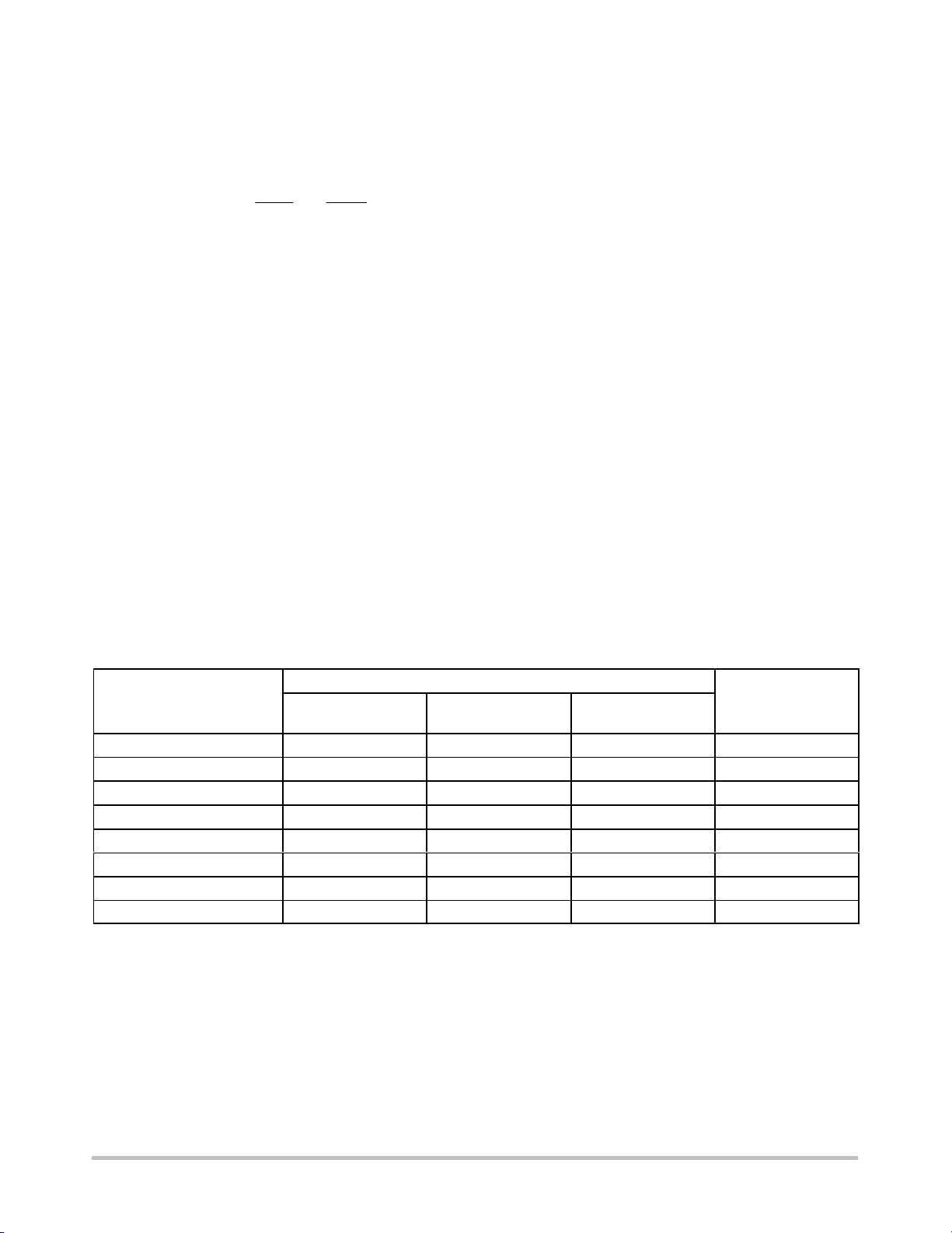
Table 1. FAST CHARGE BACKUP TERMINATION TIME/TEMPERATURE LIMIT
Backup
Termination
Mode
Time Open Open Open 283
Time Open Open GND 247
Time Open GND Open 212
Time Open GND GND 177
Time GND Open Open 141
Time GND Open GND 106
Time GND GND Open 71
Temperature 0 V to VCC − 0.7 V 0 V to VCC − 0.7 V 0 V to VCC − 0.7 V Timer Disabled
t3/T
(Pin 5)
ref
Low
Programming Inputs
t2/T
sen
(Pin 6)
t1/T
High
ref
(Pin 7)
Time Limit
Fast Charge
(Minutes)
http://onsemi.com
8
Page 9

MC33340, MC33342
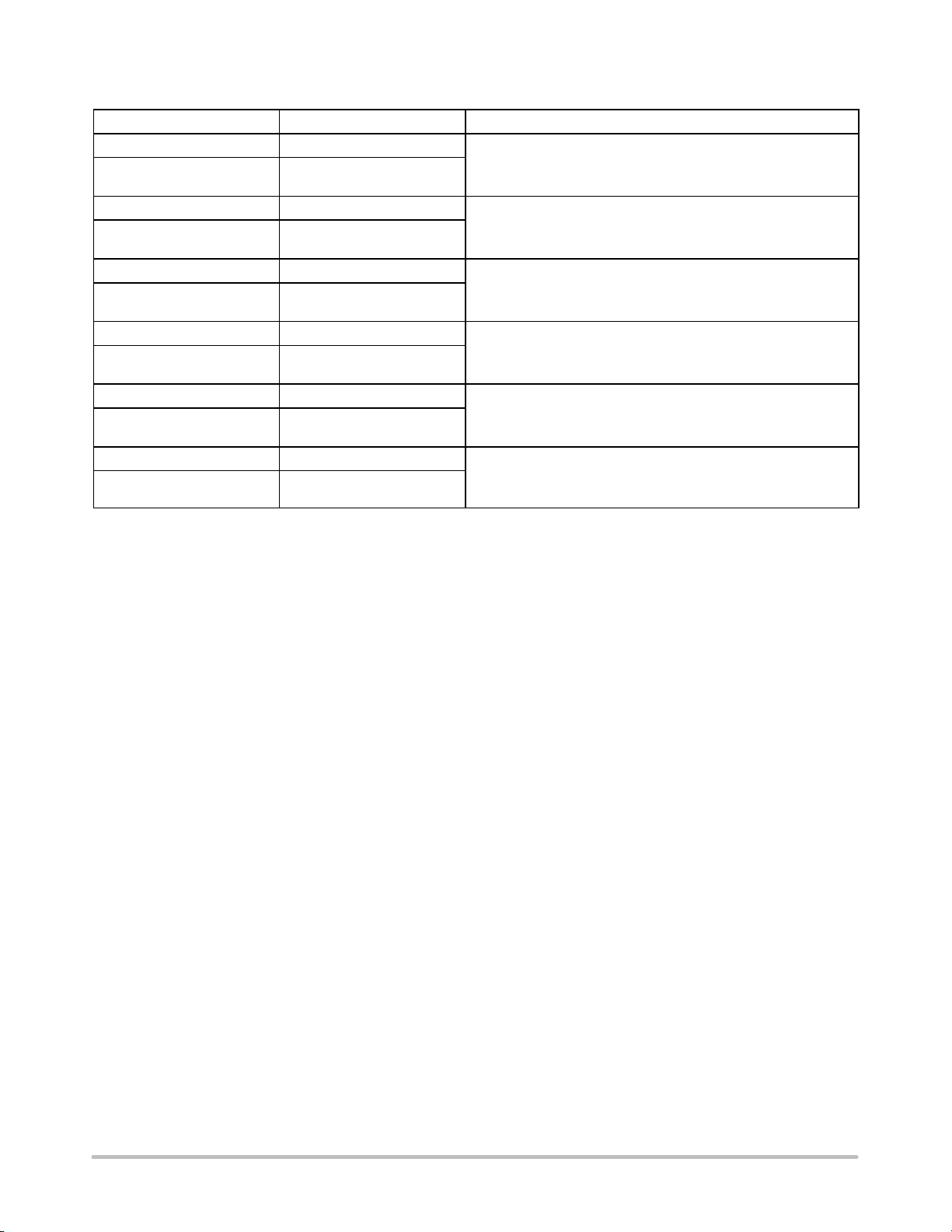
Table 2. CONTROLLER OPERATING MODE TABLE
Input Condition Controller Operation
V
Input Voltage:
sen
>1.0 V and <2.0 V
>1.0 V and <2.0 V with
two consecutive −DV
events detected after the
initial holdoff period
<1.0 V or >2.0 V The divided down battery pack voltage is outside of the fast charge voltage range. The charger
Timer Backup:
Within time limit
Beyond time limit The timer has exceeded the programmed limit. The charger switches from fast to a latched
Temperature Backup:
Within limits
Below lower limit The battery pack temperature is below the programmed lower limit. The charger will stay in trickle
Above upper limit The battery pack temperature has exceeded the programmed upper limit. The charger switches from
Power Supply Voltage:
VCC >3.0 V and <18 V
VCC >0.6 V and <2.8 V The undervoltage lockout comparator will be activated and the charger will be in trickle mode. A reset
(t
hold
The divided down battery pack voltage is within the fast charge voltage range. The charger switches
from trickle to fast charge mode as V
the timer and the overtemperature latch.
The battery pack has reached full charge and the charger switches from fast to a latched trickle mode.
A reset pulse must be applied for the charger to switch back to the fast mode. The reset pulse occurs
when entering the 1.0 V to 2.0 V window for V
)
switches from fast to trickle mode.
The timer has not exceeded the programmed limit. The charger will be in fast charge mode if V
VCC are within their respective operating limits.
trickle mode.
The battery pack temperature is within the programmed limits. The charger will be in fast charge mode
if V
and VCC are within their respective operating limits.
sen
mode until the lower temperature limit is exceeded. When exceeded, the charger will switch from trickle
to fast charge mode.
fast to a latched trickle mode. A reset signal must be applied and then released for the charger to
switch back to the fast charge mode. The reset pulse occurs when entering the 1.0 V to 2.0 V window
for V
or when VCC rises above 3.0 V.
sen
This is the nominal power supply operating voltage range. The charger will be in fast charge mode if
V
, and temperature backup or timer backup are within their respective operating limits.
sen
signal is applied to the timer and over temperature latch.
enters this voltage range, and a reset pulse is then applied to
sen
or when VCC rises above 3.0 V.
sen
sen
and
Testing
Under normal operating conditions, it would take
283 minutes to verify the operation of the 34 stage ripple
counter used in the timer. In order to significantly reduce the
test time, three digital switches were added to the circuitry
and are used to bypass selected divider stages. Entering each
of the test modes without requiring additional package pins
or affecting normal device operation proved to be
challenging. Refer to the timer functional block diagram in
Figure 11.
Switch 1 bypasses 19 divider stages to provide a 524,288
times speedup of the clock. This switch is enabled when the
V
input falls below 1.0 V. Verification of the programmed
sen
fast charge time limit is accomplished by measuring the
propagation delay from when the V
input falls below
sen
1.0 V, to when the F/T output changes from a high−to−low
state. The 71, 106, 141, 177, 212, 247 and 283 will now
correspond to 8.1, 12.1, 16.2, 20.2, 24.3, 28.3 and 32.3 ms
delays. It is possible to enter this test mode during operation
if the equivalent battery pack voltage was to fall below 1.0 V.
This will not present a problem since the device would
normally switch from fast to trickle mode under these
conditions, and the relatively short variable time delay
would be transparent to the user.
Switch 2 bypasses 11 divider stages to provide a 2048
times speedup of the clock. This switch is necessary for
testing the 19 stages that were bypassed when switch 1 was
enabled. Switch 2 is enabled when the V
1.0 V and the t1/T
High input is biased at −100 mV.
ref
input falls below
sen
Verification of the 19 stages is accomplished by measuring
a nominal propagation delay of 338.8 ms from when the V
sen
input fall s below 1.0 V, to when the F/T output changes from
a high−to−low state.
Switch 3 is a dual switch consisting of sections “A” and
“B”. Section “A” bypasses 5 divider stages to provide a 32
times speedup of the V
gate signal that is used in sampling
sen
the battery voltage. This speedup allows faster test
verification of two successive −DV events. Section “B”
bypasses 11 divider stages to provide a 2048 speedup of the
trickle mode holdoff timer. Switches 3A and 3B are both
activated when the t1/T
High input is biased at −100 mV
ref
with respect to Pin 4.
http://onsemi.com
9
Page 10

MC33340, MC33342
Q Q 22 ms Convert
D
11 ms Preset
Oscillator
760 kHz
÷2
Switch 2
11
2
3
÷2
6
÷2
2
÷2
3
÷2
1
Switch 3A
5
2
5
÷2
NormalTest
÷2
8
÷2
2
÷2 ÷2 ÷2 ÷2
Switch 3B
95 kHz
SCK to
Voltage to
Frequency
Converter
Each test mode bypass switch is shown
in the proper position for normal charger operation.
11
2
Holdoff Time Signal
Switch 1
19
2
MC33340
MC33342
t1/T
ref
t2/T
sen
t3/T
ref
High
Time and Test Decoder
Low
Fast/Trickle Output
Figure 11. Timer Functional Block Diagram
V
V
CC
30 mA
30 mA
30 mA
CC
C2
0.1
t1/T
7
t2/T
6
t3/T
5
ref
sen
ref
Battery
Pack
High
Low
SW1
SW3
V
R5
1.0 k
D3
AC
Line
Input
DC
Input
LM317
I
Adj
IC2
1N4002
D2
R7
2.4
R2
R1
V
C1
0.01
sen
1
R8
220
R6
1.8 k
D1
Charge
Status
R2 + R1
I
chg(fast)
I
chg(trickle)
This application combines the MC33340/342 with an adjustable three terminal regulator to form an isolated secondary side battery charger. Regulator IC2
operates as a constant current source with R7 setting the fast charge level. The trickle charge level is set by R5. The R2/R1 divider should be adjusted so
that the V
sinks for IC2 and are all manufactured by AAVID Engineering Inc.
input is less than 2.0 V when the batteries are fully charged. The printed circuit board shown below will accept the several TO−220 style heat-
sen
D4
V
sen
Gate
2
V
Batt
ǒ
+
V
+
sen
V
ref
–1
) (I
Vin–V
R7
Ǔ
Adj
f(D3)
R5
R8)
–V
3
Fast/
Trickle
Batt
Internal Bias
2.0 V
1.0 V
IC1 MC33340 or MC33342
Voltage to
Frequency
Converter
Ck F/V R
High
Battery
Detect
Low
−DV Detect
Counter
Timer
V
sen
Gate
F/T
Gnd
Undervoltage
Over
Under
t1
t2
t3
t/T
4
Lockout
R
Q
S
Temp
Detect
Time/Temp
Select
Over
Temp
Latch
8
CC
2.9 V
0.6 V
R
10 k
SW2
NTC
R3
R4
Figure 12. Line Isolated Linear Regulator Charger
http://onsemi.com
10
Page 11

MC33340, MC33342
Input
Return
Input
Positive
Input
AAVID #
q
SA
°C/W
592502B03400 24.0
593002B03400 14.0
590302B03600 9.2
2.25″
Charge Mode
R
R4
D1
C1
R1
D4
R5
R6
D3
IC2
321
R3
IC1
R2
R8
NTC
Output
C2
D2
R7
Battery
Negative
R
NTC
R
NTC
Battery
Positive
MC33340
1.70″
(Top View) (Bottom View)
Figure 13. Printed Circuit Board and Component Layout
(Circuit of Figure 12)
UC3842 Series
V
CC
R2
R1
Voltage
Feedback
Input
Output/
Compensation
1.0 mA
2R
2
Error
Amplifier
1
1.0 V
R
Current Sense
Comparator
Gnd 5
Primary Circuitry
Isolation Boundary
Secondary Circuitry
V
sen
Gate
R3
OC2
OC1
V
Battery
V
sen
Gate
MC33340 or MC33342
2
3
Fast/
Trickle
F/T
Gnd 4
The MC33340/342 can be combined with any of the devices in the UC3842 family of current mode controllers to form a switch mode battery charger. In this
example, optocouplers OC1 and OC2 are used to provide isolated control signals to the UC3842. During battery voltage sensing, OC2 momentarily grounds
the Output/Compensation pin, effectively turning off the charger. When fast charge termination is reached, OC1 turns on, and grounds the lower side of R3.
This reduces the peak switch current threshold of the Current Sense Comparator to a programmed trickle current level. For additional converter design information, refer to the UC3842 and UC3844 device family data sheets.
Figure 14. Line Isolated Switch Mode Charger
http://onsemi.com
11
Page 12

MC33340, MC33342
MC34166 or MC34167
I
Limit
OSC
S
Q
R
PWM
Thermal
UVLO
Gnd 3 Compensation 5
Ref
EA
C1 R3
V
sen
Gate
2
3
Fast/
Trickle
V
CC
+
4
Switch
Output
2
Voltage
Feedback
Input
1
R1
MC33340/342
R2
Battery
Pack
V
sen
Gate
F/T
AC
Line
Input
R4
Gnd 4
The MC33340/342 can be used to control the MC34166 or MC34167 power switching regulators to produce an economical and efficient fast charger. These
devices are capable of operating continuously in current limit with an input voltage range of 7.5 to 40 V. The typical charging current for the MC34166 and
MC34167 is 4.3 A and 6.5 A respectively. Resistors R2 and R1 are used to set the battery pack fast charge float voltage. If precise float voltage control is not
required, components R1, R2, R3 and C1 can be deleted, and Pin 1 must be grounded. The trickle current level is set by resistor R4. It is recommended that
a redundant charge termination method be employed for end user protection. This is especially true for fast charger systems. For additional converter design
information, refer to the MC34166 and MC34167 data sheets.
Figure 15. Switch Mode Fast Charger
http://onsemi.com
12
Page 13
MC33340, MC33342
ORDERING INFORMATION
Device Package Shipping
MC33340D SO−8
MC33340DG SO−8
(Pb−Free)
MC33340DR2 SO−8
MC33340DR2G SO−8
(Pb−Free)
MC33340P PDIP−8
MC33340PG PDIP−8
(Pb−Free)
MC33342D SO−8
MC33342DG SO−8
(Pb−Free)
MC33342DR2 SO−8
MC33342DR2G SO−8
(Pb−Free)
MC33342P PDIP−8
MC33342PG PDIP−8
(Pb−Free)
†For information on tape and reel specifications, including part orientation and tape sizes, please refer to our Tape and Reel Packaging
Specifications Brochure, BRD8011/D.
98 Units / Rail
2500 / Tape & Reel
1000 Units / Rail
98 Units / Rail
2500 / Tape & Reel
1000 Units / Rail
†
http://onsemi.com
13
Page 14

NOTE 2
−T−
SEATING
PLANE
H
58
−B−
14
F
−A−
C
N
D
G
0.13 (0.005) B
MC33340, MC33342
PACKAGE DIMENSIONS
PDIP−8
P SUFFIX
CASE 626−05
ISSUE L
NOTES:
1. DIMENSION L TO CENTER OF LEAD WHEN
FORMED PARALLEL.
2. PACKAGE CONTOUR OPTIONAL (ROUND OR
SQUARE CORNERS).
3. DIMENSIONING AND TOLERANCING PER ANSI
Y14.5M, 1982.
DIM MIN MAX MIN MAX
A 9.40 10.16 0.370 0.400
B 6.10 6.60 0.240 0.260
C 3.94 4.45 0.155 0.175
D 0.38 0.51 0.015 0.020
L
J
K
M
M
A
T
M
M
F 1.02 1.78 0.040 0.070
G 2.54 BSC 0.100 BSC
H 0.76 1.27 0.030 0.050
J 0.20 0.30 0.008 0.012
K 2.92 3.43 0.115 0.135
L 7.62 BSC 0.300 BSC
M −−− 10 −−− 10
N 0.76 1.01 0.030 0.040
INCHESMILLIMETERS
__
http://onsemi.com
14
Page 15

−Y−
−Z−
MC33340, MC33342
PACKAGE DIMENSIONS
SOIC−8 NB
CASE 751−07
ISSUE AG
NOTES:
−X−
A
58
B
1
S
0.25 (0.010)
4
M
M
Y
K
G
N
C
SEATING
PLANE
0.10 (0.004)
H
D
0.25 (0.010) Z
M
SXS
Y
X 45
_
M
J
1. DIMENSIONING AND TOLERANCING PER
ANSI Y14.5M, 1982.
2. CONTROLLING DIMENSION: MILLIMETER.
3. DIMENSION A AND B DO NOT INCLUDE
MOLD PROTRUSION.
4. MAXIMUM MOLD PROTRUSION 0.15 (0.006)
PER SIDE.
5. DIMENSION D DOES NOT INCLUDE DAMBAR
PROTRUSION. ALLOWABLE DAMBAR
PROTRUSION SHALL BE 0.127 (0.005) TOTAL
IN EXCESS OF THE D DIMENSION AT
MAXIMUM MATERIAL CONDITION.
6. 751−01 THRU 751−06 ARE OBSOLETE. NEW
STANDARD IS 751−07.
MILLIMETERS
DIMAMIN MAX MIN MAX
4.80 5.00 0.189 0.197
B 3.80 4.00 0.150 0.157
C 1.35 1.75 0.053 0.069
D 0.33 0.51 0.013 0.020
G 1.27 BSC 0.050 BSC
H 0.10 0.25 0.004 0.010
J 0.19 0.25 0.007 0.010
K 0.40 1.27 0.016 0.050
M 0 8 0 8
____
N 0.25 0.50 0.010 0.020
S 5.80 6.20 0.228 0.244
INCHES
SOLDERING FOOTPRINT*
1.52
0.060
7.0
0.275
0.6
0.024
*For additional information on our Pb−Free strategy and soldering
details, please download the ON Semiconductor Soldering and
Mounting Techniques Reference Manual, SOLDERRM/D.
4.0
0.155
1.270
0.050
SCALE 6:1
ǒ
inches
mm
Ǔ
http://onsemi.com
15
Page 16

MC33340, MC33342
ON Semiconductor and are registered trademarks of Semiconductor Components Industries, LLC (SCILLC). SCILLC reserves the right to make changes without further notice
to any products herein. SCILLC makes no warranty, representation or guarantee regarding the suitability of its products for any particular purpose, nor does SCILLC assume any liability
arising out of the application or use of any product or circuit, and specifically disclaims any and all liability, including without limitation special, consequential or incidental damages.
“Typical” parameters which may be provided in SCILLC data sheets and/or specifications can and do vary in different applications and actual performance may vary over time. All
operating parameters, including “Typicals” must be validated for each customer application by customer’s technical experts. SCILLC does not convey any license under its patent rights
nor the rights of others. SCILLC products are not designed, intended, or authorized for use as components in systems intended for surgical implant into the body, or other applications
intended to support or sustain life, or for any other application in which the failure of the SCILLC product could create a situation where personal injury or death may occur. Should
Buyer purchase or use SCILLC products for any such unintended or unauthorized application, Buyer shall indemnify and hold SCILLC and its officers, employees, subsidiaries, affiliates,
and distributors harmless against all claims, costs, damages, and expenses, and reasonable attorney fees arising out of, directly or indirectly, any claim of personal injury or death
associated with such unintended or unauthorized use, even if such claim alleges that SCILLC was negligent regarding the design or manufacture of the part. SCILLC is an Equal
Opportunity/Affirmative Action Employer. This literature is subject to all applicable copyright laws and is not for resale in any manner.
PUBLICATION ORDERING INFORMATION
LITERATURE FULFILLMENT:
Literature Distribution Center for ON Semiconductor
P.O. Box 61312, Phoenix, Arizona 85082−1312 USA
Phone: 480−829−7710 or 800−344−3860 Toll Free USA/Canada
Fax: 480−829−7709 or 800−344−3867 Toll Free USA/Canada
Email: orderlit@onsemi.com
N. American Technical Support: 800−282−9855 Toll Free
USA/Canada
Japan: ON Semiconductor, Japan Customer Focus Center
2−9−1 Kamimeguro, Meguro−ku, Tokyo, Japan 153−0051
Phone: 81−3−5773−3850
http://onsemi.com
ON Semiconductor Website: http://onsemi.com
Order Literature: http://www.onsemi.com/litorder
For additional information, please contact your
local Sales Representative.
MC33340/D
16
Page 17

 Loading...