

MBRD835L
Preferred Device
SWITCHMODE
Power Rectifier
DPAK Surface Mount Package
This SWITCHMODE power rectifier which uses the Schottky
Barrier principle with a proprietary barrier metal, is designed for use
as output rectifiers, free wheeling, protection and steering diodes in
switching power supplies, inverters and other inductive switching
circuits. This state of the art device has the following features:
• Low Forward Voltage
• 125°C Operating Junction Temperature
• Epoxy Meets UL94, VO at 1/8″
• Compact Size
• Lead Formed for Surface Mount
Mechanical Characteristics
• Case: Epoxy, Molded
• Weight: 0.4 gram (approximately)
• Finish: All External Surfaces Corrosion Resistant and Terminal
Leads are Readily Solderable
• Lead and Mounting Surface Temperature for Soldering Purposes:
260°C Max. for 10 Seconds
• Shipped 75 units per plastic tube
• Available in 16 mm Tape and Reel, 2500 units per 13″ reel, by
adding a “T4” suffix to the part number
• Marking: B835L
MAXIMUM RATINGS
Rating Symbol Value Unit
Peak Repetitive Reverse Voltage
Working Peak Reverse Voltage
DC Blocking Voltage
Average Rectified Forward Current
(At Rated V
Peak Repetitive Forward Current
(At Rated V
20 kHz, T
Non–Repetitive Peak Surge Current
(Surge Applied at Rated Load
Conditions Halfwave, Single
Phase, 60 Hz)
Repetitive Avalanche Current
(Current Decaying Linearly to Zero in
1 s, Frequency Limited by T
Storage Temperature Range T
Operating Junction Temperature T
Voltage Rate of Change (Rated VR) dv/dt 10,000 V/s
, TC = 88°C)
R
, Square Wave,
R
= 80°C)
C
Jmax
V
RRM
V
RWM
V
R
I
F(AV)
I
FRM
I
FSM
I
AR
)
stg
J
35 V
8.0 A
16 A
75 A
2.0 A
–65 to +150 °C
–65 to +125 °C
http://onsemi.com
SCHOTTKY BARRIER
RECTIFIER
8.0 AMPERES
35 VOLTS
1
3
1
3
DPAK
CASE 369A
STYLE 3
MARKING DIAGRAM
B835L
B835L = Device Code
ORDERING INFORMATION
Device Package Shipping
MBRD835L DPAK 75 Units/Rail
MBRD835LT4 DPAK 2500/Tape & Reel
Preferred devices are recommended choices for future use
and best overall value.
4
4
Semiconductor Components Industries, LLC, 2000
October, 2000 – Rev. 2
1 Publication Order Number:
MBRD835L/D
MBRD835L
)
THERMAL CHARACTERISTICS
Rating Symbol Value Unit
Thermal Resistance — Junction to Case R
Thermal Resistance — Junction to Ambient (Note 1.) R
ELECTRICAL CHARACTERISTICS
Maximum Instantaneous Forward Voltage (Note 2.) (iF = 8 Amps, TC = +25°C)
Maximum Instantaneous Reverse Current (Note 2.) (Rated dc Voltage, TC = +25°C)
1. Rating applies when surface mounted on the minimum pad size recommended.
2. Pulse Test: Pulse Width = 300 µs, Duty Cycle ≤ 2%.
(i
= 8 Amps, TC = +125°C)
F
(Rated dc Voltage, T
= +100°C)
C
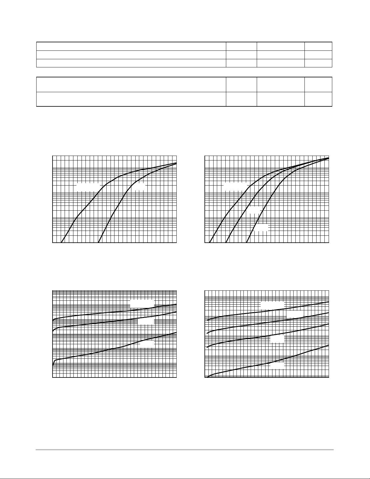
TYPICAL CHARACTERISTICS
θ
JC
θ
JA
V
F
6 °C/W
80 °C/W
0.51
Volts
0.41
I
R
1.4
mA
35
10
T
= 125°C
1
J
25°C
0.1
, INSTANTANEOUS FORWARD CURRENT (mA)
0.01
F
i
0.1 0.2 0.3 0.4 0.5
0 0.6
v
, INSTANTANEOUS VOLTAGE (VOLTS)
F
Figure 1. Maximum Forward Voltage Figure 2. Typical Forward Voltage
1000
= 125°C
T
100
, REVERSE CURRENT (mA)
R
I
0.01
10
1
0.1
J
100°C
25°C
10
T
= 125°C
J
1
75°C
0.1
0.01
, INSTANTANEOUS FORWARD CURRENT (AMPS
F
I
0.1 0.2 0.3 0.4 0.5
0 0.6
V
, INSTANTANEOUS VOLTAGE (VOLTS)
F
25°C
100
T
= 125°C
J
100°C
75°C
, REVERSE CURRENT (mA)
R
I
10
1
0.1
25°C
0.001
5101520
035
, REVERSE VOLTAGE (VOLTS)
V
F
25 30 25 30 35
0.01
5101520
0
V
, REVERSE VOLTAGE (VOLTS)
R
Figure 3. Maximum Reverse Current Figure 4. Typical Reverse Current
http://onsemi.com
2

1000
C, CAPACITANCE (pF)
MBRD835L
TYPICAL CHARACTERISTICS
T
= 25°C
J
TYPICAL
MAXIMUM
100
1
Figure 5. Maximum and T ypical Capacitance
16
14.4
12.8
11.2
9.6
8
dc
SQUARE WAVE
T
= 125°C
J
π (RESISTIVE LOAD)
R
θ
JA
PK
AV
5
(CAPACITIVE
I
I
6.4
4.8
3.2
, AVERAGE FORWARD CURRENT (AMPS)
1.6
F(AV)
I
0
80 130
85 90 95 100 105 110 115 120 125
10
20
T
, CASE TEMPERATURE (°C)
C
Figure 6. Current Derating, Infinite Heatsink Figure 7. Current Derating
V
, REVERSE VOLTAGE (VOLTS)
R
= 6°C/W
LOAD)
, AVERAGE FORWARD CURRENT (AMPS)
F(AV)
I
10
8
7
6
π (RESISTIVE LOAD)
5
4
= 125°C
J
dc
SQUARE WAVE
R
= 40°C/W
θ
JA
SURFACE MOUNTED ON
MININUM RECOMMENDED
PAD SIZE
PK
AV
5
(CAPACITIVE
LOAD)
I
I
T
3
2
1
0
0 130
10
20
5010 20 30 40 8060 70 10090 110 120
T
, AMBIENT TEMPERATURE (°C)
A
5
4.5
4
3.5
3
2.5
2
1.5
1
, AVERAGE FORWARD CURRENT (AMPS)
0.5
F(AV)
I
0
0
T
dc
π
(RESISTIVE LOAD)
SQUARE WAVE
= 125°C
J
R
= 80°C/W
θ
JA
SURFACE MOUNTED ON
MININUM RECOMMENDED
PAD SIZE
PK
AV
5
(CAPACITIVE
LOAD)
I
I
T
= 125°C
J
7
I
PK
6
5
I
AV
π (RESISTIVE LOAD)
(CAPACITIVE
LOAD)
SQUARE WAVE
5
4
10
20
3
8
10
20
10
, AMBIENT TEMPERATURE (°C)
T
A
1305020 30 40 8060 70 10090 110 120
, AVERAGE FORWARD POWER DISSIPATION (WATTS)
F(AV)
P
2
1
0
0
1.5 3 4.5 6
7.5 9 10.5 12 13.5 15
I
, AVERAGE FORWARD CURRENT (AMPS)
F(AV)
Figure 8. Current Derating, Free Air Figure 9. Forward Power Dissipation
http://onsemi.com
3
dc

MBRD835L
PACKAGE DIMENSIONS
DPAK
PLASTIC
CASE 369A–13
SEATING
–T–
PLANE
B
V
S
R
4
A
123
K
F
L
D
2 PL
G
C
J
H
0.13 (0.005) T
M
E
U
ISSUE AA
0.165
4.191
0.100
Z
0.118
3.0
2.54
0.063
1.6
0.190
4.826
DPAK FOOTPRINT
NOTES:
1. DIMENSIONING AND TOLERANCING PER ANSI
Y14.5M, 1982.
2. CONTROLLING DIMENSION: INCH.
DIM MIN MAX MIN MAX
A 0.235 0.250 5.97 6.35
B 0.250 0.265 6.35 6.73
C 0.086 0.094 2.19 2.38
D 0.027 0.035 0.69 0.88
E 0.033 0.040 0.84 1.01
F 0.037 0.047 0.94 1.19
G 0.180 BSC 4.58 BSC
H 0.034 0.040 0.87 1.01
J 0.018 0.023 0.46 0.58
K 0.102 0.114 2.60 2.89
L 0.090 BSC 2.29 BSC
R 0.175 0.215 4.45 5.46
S 0.020 0.050 0.51 1.27
U 0.020 --- 0.51 ---
V 0.030 0.050 0.77 1.27
Z 0.138 --- 3.51 ---
STYLE 3:
PIN 1. ANODE
2. CATHODE
3. ANODE
4. CATHODE
0.243
6.172
inches
mm
MILLIMETERSINCHES
SWITCHMODE is a trademark of Semiconductor Components Industries, LLC.
ON Semiconductor and are trademarks of Semiconductor Components Industries, LLC (SCILLC). SCILLC reserves the right to make changes
without further notice to any products herein. SCILLC makes no warranty, representation or guarantee regarding the suitability of its products for any particular
purpose, nor does SCILLC assume any liability arising out of the application or use of any product or circuit, and specifically disclaims any and all liability,
including without limitation special, consequential or incidental damages. “Typical” parameters which may be provided in SCILLC data sheets and/or
specifications can and do vary in different applications and actual performance may vary over time. All operating parameters, including “Typicals” must be
validated for each customer application by customer’s technical experts. SCILLC does not convey any license under its patent rights nor the rights of others.
SCILLC products are not designed, intended, or authorized for use as components in systems intended for surgical implant into the body, or other applications
intended to support or sustain life, or for any other application in which the failure of the SCILLC product could create a situation where personal injury or
death may occur. Should Buyer purchase or use SCILLC products for any such unintended or unauthorized application, Buyer shall indemnify and hold
SCILLC and its officers, employees, subsidiaries, affiliates, and distributors harmless against all claims, costs, damages, and expenses, and reasonable
attorney fees arising out of, directly or indirectly, any claim of personal injury or death associated with such unintended or unauthorized use, even if such claim
alleges that SCILLC was negligent regarding the design or manufacture of the part. SCILLC is an Equal Opportunity/Affirmative Action Employer.
PUBLICATION ORDERING INFORMATION
NORTH AMERICA Literature Fulfillment:
Literature Distribution Center for ON Semiconductor
P.O. Box 5163, Denver, Colorado 80217 USA
Phone: 303–675–2175 or 800–344–3860 Toll Free USA/Canada
Fax: 303–675–2176 or 800–344–3867 Toll Free USA/Canada
Email: ONlit@hibbertco.com
Fax Response Line: 303–675–2167 or 800–344–3810 Toll Free USA/Canada
N. American Technical Support: 800–282–9855 Toll Free USA/Canada
EUROPE: LDC for ON Semiconductor – European Support
German Phone: (+1) 303–308–7140 (Mon–Fri 2:30pm to 7:00pm CET)
Email: ONlit–german@hibbertco.com
French Phone: (+1) 303–308–7141 (Mon–Fri 2:00pm to 7:00pm CET)
Email: ONlit–french@hibbertco.com
English Phone: (+1) 303–308–7142 (Mon–Fri 12:00pm to 5:00pm GMT)
Email: ONlit@hibbertco.com
EUROPEAN TOLL–FREE ACCESS*: 00–800–4422–3781
*Available from Germany, France, Italy, UK, Ireland
CENTRAL/SOUTH AMERICA:
Spanish Phone: 303–308–7143 (Mon–Fri 8:00am to 5:00pm MST)
Email: ONlit–spanish@hibbertco.com
Toll–Free from Mexico: Dial 01–800–288–2872 for Access –
then Dial 866–297–9322
ASIA/PACIFIC: LDC for ON Semiconductor – Asia Support
Phone: 303–675–2121 (Tue–Fri 9:00am to 1:00pm, Hong Kong Time)
Toll Free from Hong Kong & Singapore:
001–800–4422–3781
Email: ONlit–asia@hibbertco.com
JAPAN: ON Semiconductor, Japan Customer Focus Center
4–32–1 Nishi–Gotanda, Shinagawa–ku, Tokyo, Japan 141–0031
Phone: 81–3–5740–2700
Email: r14525@onsemi.com
ON Semiconductor Website: http://onsemi.com
For additional information, please contact your local
Sales Representative.
http://onsemi.com
4
MBRD835L/D

 Loading...