

LC03-6R2
Low Capacitance Surface
Mount TVS for High-Speed
Data Interfaces
The LC03-6 transient voltage suppressor is designed to protect
equipment attached to high speed communication lines from ESD,
EFT, and lighting.
http://onsemi.com
Features
•SO-8 Package
•Peak Power - 2000 Watts 8 x 20 mS
•ITU K.20 I
= 40 A (5/310 ms)
PP
•Bellcore 1089 (Intra-Building) 100 A (2/10 ms)
•ESD Rating:
IEC 61000-4-2 (ESD) 15 kV (air) 8 kV (contact)
IEC 61000-4-4 (EFT) 40 A (5/50 ns)
IEC 61000-4-5 (lighting) 95 A (8/20 ms)
•UL Flammability Rating of 94 V-0
•Pb-Free Package is Available
Typical Applications
•High Speed Communication Line Protection
MAXIMUM RATINGS
Rating Symbol Value Unit
Peak Power Dissipation
8 x 20 mS @ T
Peak Pulse Current (8 x 20 mS Waveform)
Junction and Storage Temperature Range TJ, T
Lead Solder Temperature Maximum 10 Seconds Duration
Stresses exceeding Maximum Ratings may damage the device. Maximum
Ratings are stress ratings only. Functional operation above the Recommended
Operating Conditions is not implied. Extended exposure to stresses above the
Recommended Operating Conditions may affect device reliability.
1. Non-repetitive current pulse 8 x 20 mS exponential decay waveform
= 25°C (Note 1)
A
P
pk
I
PP
stg
T
L
2000 W
100 A
- 55 to +150 °C
260 °C
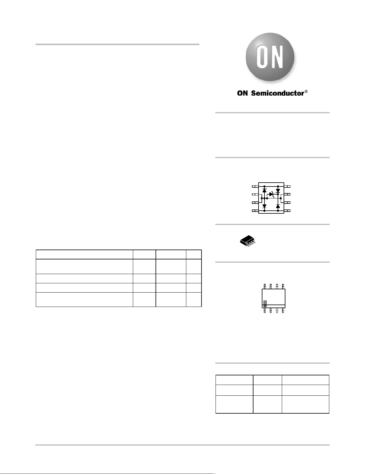
SO-8 LOW CAPACITANCE
VOLTAGE SUPPRESSOR
2 kW PEAK POWER
6 VOLTS
PIN CONFIGURATION
AND SCHEMATIC
1
2
3
4
8
1
MARKING DIAGRAM
8
LC036
AYWWG
G
1
LC036 = Device Code
A = Assembly Location
Y = Year
WW = Work Week
G = Pb-Free Package
(Note: Microdot may be in either location)
8
7
6
5
SOIC-8
CASE 751
PLASTIC
© Semiconductor Components Industries, LLC, 2007
June, 2007 - Rev. 4
ORDERING INFORMATION
Device Package
LC03-6R2 SO-8 2500/Tape & Reel
LC03-6R2G SO-8
(Pb-Free)
†For information on tape and reel specifications,
including part orientation and tape sizes, please
refer to our Tape and Reel Packaging Specification
Brochure, BRD8011/D.
1 Publication Order Number:
Shipping
2500/Tape & Reel
†
LC03-6R2/D
LC03-6R2
ELECTRICAL CHARACTERISTICS
Characteristic Symbol Min Typ Max Unit
Reverse Breakdown Voltage @ It = 1.0 mA V
Reverse Leakage Current @ V
= 5.0 V I
RWN
Maximum Clamping Voltage @ IPP = 50 A, 8 x 20 mS
Maximum Clamping Voltage @ IPP = 100 A, 8 x 20 mS
BR
R
V
C
V
C
Between I/O Pins and Ground @ VR = 0 V, 1.0 MHz Capacitance - 16 25 pF
Between I/O Pins @ VR = 0 Volts, 1.0 MHz Capacitance - 8.0 12 pF
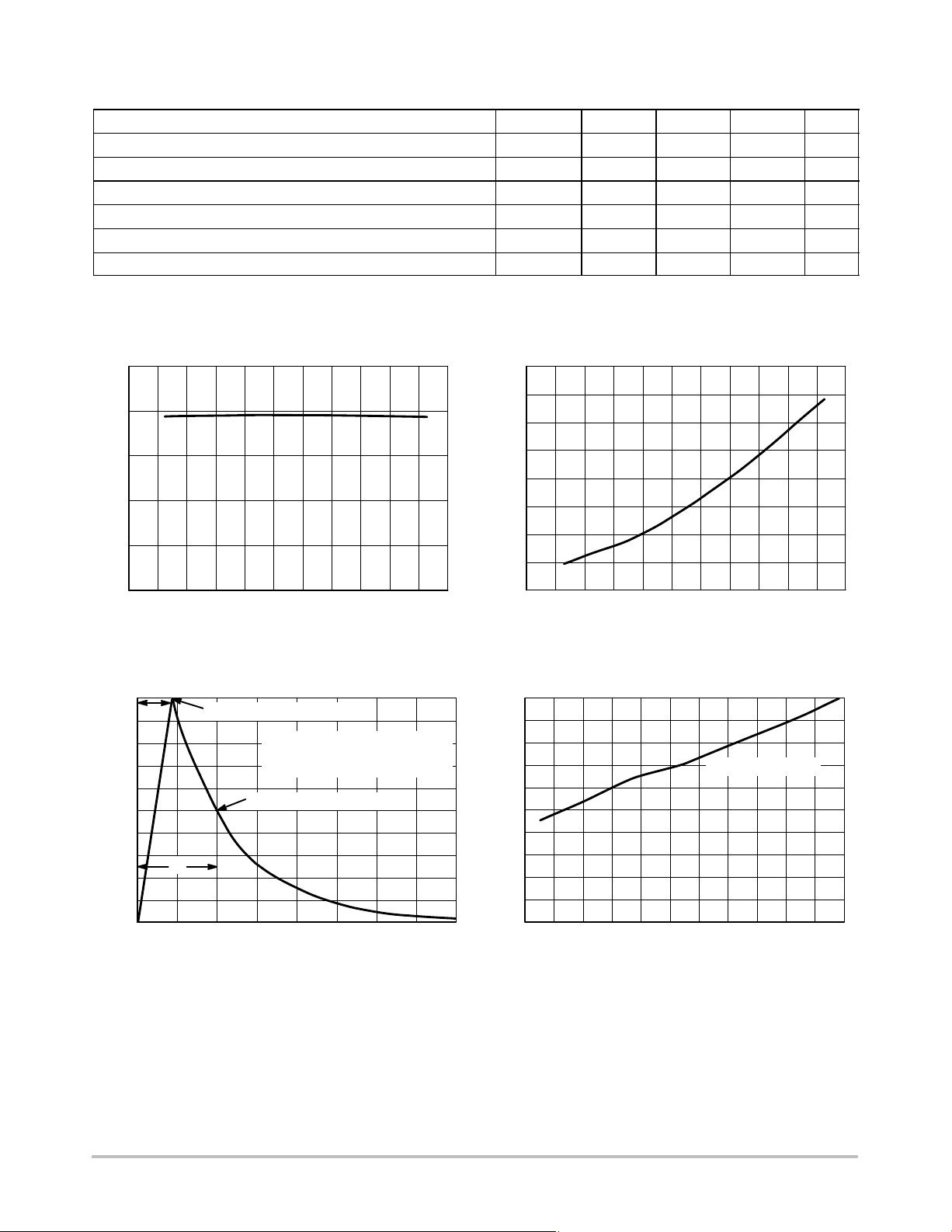
TYPICAL CHARACTERISTICS
6.8 - - V
N/A - 20
N/A - 15 V
N/A - 20 V
mA
10
8
6
4
, REVERSE VOLTAGE (V)
Z
2
V
0
-80 0
-40
-60 20-20 10060
40 120
80 140
T, TEMPERATURE (°C)
Figure 1. Reverse Voltage versus Temperature
100
90
80
70
60
50
t
r
PEAK VALUE I
PULSE WIDTH (tP) IS DEFINED
AS THAT POINT WHERE THE
PEAK CURRENT DECAY = 8 ms
HALF VALUE I
RSM
@ 8 ms
RSM
/2 @ 20 ms
40
30
20
% OF PEAK PULSE CURRENT
10
0
t
P
0204060
t, TIME (ms)
Figure 3. 8 x 20 ms Pulse Waveform
80
16
14
12
10
8
6
4
, REVERSE LEAKAGE (mA)
R
I
2
0
-80 -60 20 100
-40 -20 40 60 80
0 120
T, TEMPERATURE (°C)
Figure 2. Reverse Leakage versus
Temperature
20
18
16
14
8 x 20 ms Waveform
12
10
8
6
, CLAMPING VOLTAGE (V)
4
C
V
2
0
0204060
10 30 50 70 11090 100
, PEAK PULSE CURRENT (A)
I
PP
80
Figure 4. Clamping Voltage versus Peak Pulse
Current
140
http://onsemi.com
2

LC03-6R2
APPLICATIONS INFORMATION
The LC03- 6 ON Semiconductor's device is a TVS Diode
array designed to protect sensitive electronics such as
communications systems, computers, and computer
peripherals against damage due to transient overvoltage
conditions caused by lightning, electrostatic discharge
(ESD), and electrical fast transients (EFT). Because of its
relative low capacitance (<25 pf), it can be used in high speed
I/O data lines such as USB 1.1 ports.
The integrated design of the LC03-6 device offers high
surge rating, low capacitance steering diodes, and a TVS
diode integrated in a single package (SO-8). In addition, this
device offers compliance to Bellcore 1089 requirements
(intra-building).
LC03-6 Device's Configurations Options
Protection of Two High-speed I/O Data Lines
The LC03-6 device is able to protect two high speed data
lines against transient overvoltage conditions by driving
them to a fixed reference point for clamping purposes.
Depending in the application's requirements, the LC03-6
device can be configured for protection in either differential
mode (Line-to-Line) or common mode (Line-to-ground).
The Figure 5 shows the connection for Differential mode
(Line-to-Line) and Common mode (Line-to-Ground)
protection. The inputs and outputs of the I/O data lines are
connected at terminals 1 to 8, and 4 to 5 while the terminals
2, 3, 6 and 7 are connected to ground; for better performance,
it is recommended to minimize parasitic inductances by
using ground planes and minimizing the PCB trace lengths
for the ground return connections.
If differential protection is required by some particular
applications, then the configuration for differential protection
is made as shown in the Figure 6:
LC03-6
Line 1
In
N/C
N/C
Line 2
In
Figure 6. Configuration for Differential
Protection (Line-to-Line)
T1/E1 Linecard Protection (Intra-Building)
N/C
N/C
Line 1
Out
Line 2
Out
The Figure 7 shows a typical schematic for a T1/E1 line
card protection circuit. The LC03- 6 device is connected
between Tip and Ring on the transmit and receive line pairs.
it provides protection to metallic and common mode lightning
surges per Bellcore 1089 intra- building (For further
information, see Bellcore 1089 standard). A metallic voltage
is defined as a difference of potential between the T and R
terminals of a telecommunications pair. Currents caused by
lightning, in the absence of protector operation and with
balanced terminal equipment and telecommunications loop,
cause Tip and Ring conductors to attain the same potential
hence do not produce metallic transients. Common mode
surges are suppressed by the isolation of the transformer.
LC03-6
Line 1
In
Line 2
In
Figure 5. Configuration for Differential
and Common Mode Protection
Line 1
Out
Line 2
Out
http://onsemi.com
3

LC03-6R2
PTC
RTIP
R1
R3
R2
RRING
T1/E1
TRANSCEIVER
R4
TTIP
R5
TRING
Figure 7. Typical T1 Line Card Protection
ESD Protection in USB 1.1 Port Applications
As we know, a USB port is composed of four lines. The
lines D+ and D- are used for bi-directional data
transmission, and the remaining two lines are reserved for
bus voltage and ground. Since USB is a hot plugging and
unplugging system, all its four lines have the risk to receive
ESD conditions in the real field of the application.
Typical ESD protection techniques are commonly formed
by the combination of different discrete semiconductor
products which make this technique obsolete and
non-ef ficient because the interconnections of the discrete
devices increase the parasitic inductance effects during a
LC03-6
T1
LC03-6
T2
PTC
PTC
PTC
transient condition which reduces significantly the
performance of the ESD protection circuit. The LC03-6
device provides a unique TVS Diode array designed to
protect two I/O data lines (single USB port) against damage
due to ESD conditions or transient voltage conditions.
Because of its low capacitance, it can be used in high speed
I/O data lines such as USB 1.1 components. In addition to its
low capacitance characteristics, the LC03-6 device from
ONSemiconductor complies with the most common
industrial standards for ESD, EFT and surge protection:
IEC61000-4-2, IEC61000-4-4, IEC61000-4-5.
http://onsemi.com
4

-Z-
-Y-
LC03-6R2
PACKAGE DIMENSIONS
SOIC-8 NB
CASE 751-07
ISSUE AH
NOTES:
-XA
58
B
1
S
0.25 (0.010)
4
M
M
Y
K
G
C
SEATING
PLANE
0.10 (0.004)
H
D
0.25 (0.010) Z
M
Y
SXS
N
X 45
_
M
J
1. DIMENSIONING AND TOLERANCING PER
ANSI Y14.5M, 1982.
2. CONTROLLING DIMENSION: MILLIMETER.
3. DIMENSION A AND B DO NOT INCLUDE
MOLD PROTRUSION.
4. MAXIMUM MOLD PROTRUSION 0.15 (0.006)
PER SIDE.
5. DIMENSION D DOES NOT INCLUDE DAMBAR
PROTRUSION. ALLOWABLE DAMBAR
PROTRUSION SHALL BE 0.127 (0.005) TOTAL
IN EXCESS OF THE D DIMENSION AT
MAXIMUM MATERIAL CONDITION.
6. 751-01 THRU 751-06 ARE OBSOLETE. NEW
STANDARD IS 751-07.
MILLIMETERS
DIMAMIN MAX MIN MAX
4.80 5.00 0.189 0.197
B 3.80 4.00 0.150 0.157
C 1.35 1.75 0.053 0.069
D 0.33 0.51 0.013 0.020
G 1.27 BSC 0.050 BSC
H 0.10 0.25 0.004 0.010
J 0.19 0.25 0.007 0.010
K 0.40 1.27 0.016 0.050
M 0 8 0 8
____
N 0.25 0.50 0.010 0.020
S 5.80 6.20 0.228 0.244
INCHES
SOLDERING FOOTPRINT*
1.52
0.060
7.0
0.275
0.6
0.024
*For additional information on our Pb-Free strategy and soldering
details, please download the ON Semiconductor Soldering and
Mounting Techniques Reference Manual, SOLDERRM/D.
ON Semiconductor and are registered trademarks of Semiconductor Components Industries, LLC (SCILLC). SCILLC reserves the right to make changes without further notice
to any products herein. SCILLC makes no warranty, representation or guarantee regarding the suitability of its products for any particular purpose, nor does SCILLC assume any liability
arising out of the application or use of any product or circuit, and specifically disclaims any and all liability, including without limitation special, consequential or incidental damages.
“Typical” parameters which may be provided in SCILLC data sheets and/or specifications can and do vary in different applications and actual performance may vary over time. All
operating parameters, including “Typicals” must be validated for each customer application by customer's technical experts. SCILLC does not convey any license under its patent rights
nor the rights of others. SCILLC products are not designed, intended, or authorized for use as components in systems intended for surgical implant into the body, or other applications
intended to support or sustain life, or for any other application in which the failure of the SCILLC product could create a situation where personal injury or death may occur. Should
Buyer purchase or use SCILLC products for any such unintended or unauthorized application, Buyer shall indemnify and hold SCILLC and its officers, employees, subsidiaries, affiliates,
and distributors harmless against all claims, costs, damages, and expenses, and reasonable attorney fees arising out of, directly or indirectly, any claim of personal injury or death
associated with such unintended or unauthorized use, even if such claim alleges that SCILLC was negligent regarding the design or manufacture of the part. SCILLC is an Equal
Opportunity/Affirmative Action Employer. This literature is subject to all applicable copyright laws and is not for resale in any manner.
4.0
0.155
1.270
0.050
SCALE 6:1
ǒ
inches
mm
Ǔ
PUBLICATION ORDERING INFORMATION
LITERATURE FULFILLMENT:
Literature Distribution Center for ON Semiconductor
P.O. Box 5163, Denver, Colorado 80217 USA
Phone: 303-675-2175 or 800-344-3860 Toll Free USA/Canada
Fax: 303-675-2176 or 800-344-3867 Toll Free USA/Canada
Email: orderlit@onsemi.com
N. American Technical Support: 800-282-9855 Toll Free
USA/Canada
Europe, Middle East and Africa Technical Support:
Phone: 421 33 790 2910
Japan Customer Focus Center
Phone: 81-3-5773-3850
http://onsemi.com
5
ON Semiconductor Website: www.onsemi.com
Order Literature: http://www.onsemi.com/orderlit
For additional information, please contact your local
Sales Representative
LC03-6R2/D

 Loading...